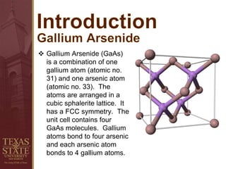
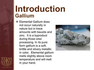
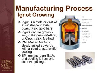
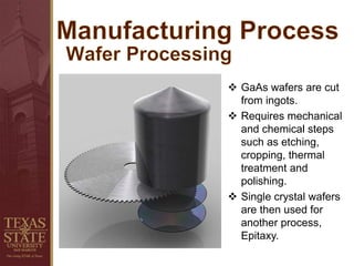
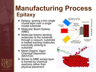
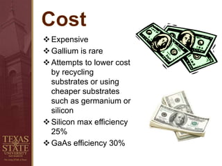
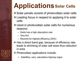
By:
Nhi Mai, Ricardo Lopez, Eric Leal,
Hector Leal Brol, James Lillian
ENGR2300 – Materials Engineering
November 2011
 Introduction
 History
 Properties
 Manufacturing Processes
 Cost
 Applications
 Conclusion
 Gallium Arsenide (GaAs)
is a combination of one
gallium atom (atomic no.
31) and one arsenic atom
(atomic no. 33). The
atoms are arranged in a
cubic sphalerite lattice. It
has a FCC symmetry. The
unit cell contains four
GaAs molecules. Gallium
atoms bond to four arsenic
and each arsenic atom
bonds to 4 gallium atoms.
 Elemental Gallium does
not occur naturally in
nature but in trace
amounts with bauxite and
zinc. It is a byproduct
during those ores’
processing. In its pure
form gallium is a soft,
brittle and silvery metallic
in color. Elemental gallium
melts slightly above room
temperature and will melt
in your hand.
 Arsenic is a highly toxic
element that is found
with many minerals,
especially sulfur, and
can be found naturally
as a pure substance.
Its main industrial use
is as a strengthener in
alloys with copper and
lead. Arsenic is also in
declining use in
pesticides and
herbicides.
 Dmitri Mendeleev
predicted all
elements’
properties on the
periodic table
 1875, Lecoq de
Boibaudran
discovered Gallium
in the Pyrenees
Mountains
 Method to retrieve
Gallium:
electrolysis
 Been known since
the Bronze Age
 1250, discovered
by Albert the Great
 Used as an
impurity in bronze
 Later found that
Arsenic was
poisonous
 Has symptoms that
were difficult to
distinguish
 Discovered by Victor
Goldschmidt
 First to combine these
elements
 1954, produced a large
amount for research on
use of this compound
 Since 1960s, used in
many devices such as
solar cells, light-emitting
diodes, lasers, and
optoelectronic devices
 Gallium, a poor metal, has atomic number 31 and it
is located in group 13, period 4, and block “p”. Its
mas is 69.72 amu, and has no electronegativity
according to Pauling.
 Arsenic, a metalloid, has atomic number 33 and it is
located in group 15, period 4, and block “p”. Its mas
is 74.92 amu, and has an electronegativity of 2.18
according to Pauling.
Electrical Properties
 Band gap (eV) = 1.42
 Electrical conductivity
1X10⁻⁶ (Ω*m)-1
 Electron mobility 7.7 m2 /
V*s
 Hole mobility .07 m2 / V*s
 Electron thermal velocity
4.4X10⁵ m/s
 Hole thermal velocity
1.8X10⁵ m/s
Thermal Properties
 GaAs has a thermal
conductivity of 0.55 W/cm-
C
 Melting point 1238 °C
 Specific heat 0.33 J g-1°C
-1
 Thermal diffusivity 0.31
cm2s-1
 Thermal expansion, linear
5.73X10⁻⁶ °C -1
The GaAs crystal is
composed of two
sublattices.
Each sublattice are face
centered cubic (fcc)
lattice.
They offset with respect
to each other by half the
diagonal of the fcc cube.
This crystal
configuration is known
as cubic sphalerite or
zinc blende.
 GaAs has basically
outdone silicon in
every imaginable
way due to its
incredible
characteristics.
 These
characteristics
make GaAs and
ideal candidate for
use in mobile
phones, satellite
communications,
microwave point-to-
point links, and
some radar
systems.
GaAs Properties
(Room
Temperature)
GaAs
 Higher saturated
electron velocity and
higher electron mobility.
 GaAs devices generate
less noise than silicon
and have higher
breakdown voltages.
 It has a direct bandgap
which means that it can
be used to emit light.
Silicon
 Considerably cheaper
than GaAs
 Existence of silicon
dioxide (one of the best
known insulators of any
kind)
 Posses a much higher
hole mobility which allows
for the construction of
higher-speed P-channel
field effect transistors.
 Ingot is a mold or cast of
a substance in bulk
quantity ex: gold bars
 Ingots can be grown 2
ways: Bridgman Method,
or Czochralski Method
 CM: Molten GaAs is
slowly pulled upwards
with a seed crystal while
cooling
 BM: melting pure GaAs
and cooling it from one
side. No pulling.
Centromax.net
 GaAs wafers are cut
from ingots.
 Requires mechanical
and chemical steps
such as etching,
cropping, thermal
treatment and
polishing.
 Single crystal wafers
are then used for
another process,
Epitaxy.
 Epitaxy- gowing a thin single
crystal layer over a single
crystal substrate
 Molecular Beam Epitaxy
(MBE)
 Molecular beams sending
molecules to the substrate
through a vacuum, substrate
is heated exciting molecules
eventually sticking to
substrate
 Metal Organic Vapor
Chemical Deposition
(MOVCD)
 Similar to MBE except layer
is formed by chemical
reactions rather than
physical placement
Expensive
Gallium is rare
Attempts to lower cost
by recycling
substrates or using
cheaper substrates
such as germanium or
silicon
Silicon max efficiency
25%
GaAs efficiency 30%
 Limit cost
 Improve integrated circuits in all
aspects of technologies.
 Due to its unique qualities, GaAs
can be used in computers, lasers,
solar cells, aerospace technology,
medical devices etc.
Solar panels consist of photovoltaic solar cells
Leading focus in respect to applying it to solar
cells
Used in photovoltaic solar cells for numerous
reasons:
– GaAs has a high absorption rate
– Very thin
– Records for highest efficiency (25%)
 Has a direct band gap, because of efficiency rate,
leads to shrinking of solar cell sizes thus reduction
in area
 Photovoltaic applications include:
– Satellites, cars, calculators highway signs
Projects such as the Rovers Spirit and
opportunity, which are exploring Mars’ surface,
have used GaAs for its solar cell power source
Radiation hardness. “Single effect events,”
(SEEs) associated with the transit of heavy ions
through semiconductor junctions have to be
minimized to reduce failure risk. Radiation
effects from particles can cause degradation,
and also failure of the electronic systems in
space vehicles or satellites
GaAs has promising future aerospace
applications in satellites, space crafts, signal
devices, sensors
Having a higher electron mobility, this allows
flow of electricity in transistors to flow much
faster and can lead to many future
applications such as:
– faster computers
– better wireless communication devices
Faster response times for transistors from
GaAs
Less propagation delay, less noise to date
using molecular beam epitaxial GaAs FETs
 GaAs power amplifiers operate at higher power
levels, have higher linearity and sharper edges,
can be operated at higher power levels because
they have higher breakdown voltages and allow
maximum channels to be used
 More efficient solar cells
 GaAs technologies allows to design at lower
frequencies, with less power consumption, over a
smaller area, providing a size and power
advantage to multi-function integrated solutions
for circuits and many more technologies
 Cost expensive, but hopefully will decrease over
the years
 GaAs has excellent electronic properties.
(It is superior to Silicon.)
 Powerful in the electronic industry:
 Aerospace
 Transistors
 Solar Cells

GaAs

  • 1.
    By: Nhi Mai, RicardoLopez, Eric Leal, Hector Leal Brol, James Lillian ENGR2300 – Materials Engineering November 2011
  • 2.
     Introduction  History Properties  Manufacturing Processes  Cost  Applications  Conclusion
  • 3.
     Gallium Arsenide(GaAs) is a combination of one gallium atom (atomic no. 31) and one arsenic atom (atomic no. 33). The atoms are arranged in a cubic sphalerite lattice. It has a FCC symmetry. The unit cell contains four GaAs molecules. Gallium atoms bond to four arsenic and each arsenic atom bonds to 4 gallium atoms.
  • 4.
     Elemental Galliumdoes not occur naturally in nature but in trace amounts with bauxite and zinc. It is a byproduct during those ores’ processing. In its pure form gallium is a soft, brittle and silvery metallic in color. Elemental gallium melts slightly above room temperature and will melt in your hand.
  • 5.
     Arsenic isa highly toxic element that is found with many minerals, especially sulfur, and can be found naturally as a pure substance. Its main industrial use is as a strengthener in alloys with copper and lead. Arsenic is also in declining use in pesticides and herbicides.
  • 6.
     Dmitri Mendeleev predictedall elements’ properties on the periodic table  1875, Lecoq de Boibaudran discovered Gallium in the Pyrenees Mountains  Method to retrieve Gallium: electrolysis
  • 7.
     Been knownsince the Bronze Age  1250, discovered by Albert the Great  Used as an impurity in bronze  Later found that Arsenic was poisonous  Has symptoms that were difficult to distinguish
  • 8.
     Discovered byVictor Goldschmidt  First to combine these elements  1954, produced a large amount for research on use of this compound  Since 1960s, used in many devices such as solar cells, light-emitting diodes, lasers, and optoelectronic devices
  • 9.
     Gallium, apoor metal, has atomic number 31 and it is located in group 13, period 4, and block “p”. Its mas is 69.72 amu, and has no electronegativity according to Pauling.  Arsenic, a metalloid, has atomic number 33 and it is located in group 15, period 4, and block “p”. Its mas is 74.92 amu, and has an electronegativity of 2.18 according to Pauling.
  • 10.
    Electrical Properties  Bandgap (eV) = 1.42  Electrical conductivity 1X10⁻⁶ (Ω*m)-1  Electron mobility 7.7 m2 / V*s  Hole mobility .07 m2 / V*s  Electron thermal velocity 4.4X10⁵ m/s  Hole thermal velocity 1.8X10⁵ m/s Thermal Properties  GaAs has a thermal conductivity of 0.55 W/cm- C  Melting point 1238 °C  Specific heat 0.33 J g-1°C -1  Thermal diffusivity 0.31 cm2s-1  Thermal expansion, linear 5.73X10⁻⁶ °C -1
  • 11.
    The GaAs crystalis composed of two sublattices. Each sublattice are face centered cubic (fcc) lattice. They offset with respect to each other by half the diagonal of the fcc cube. This crystal configuration is known as cubic sphalerite or zinc blende.
  • 12.
     GaAs hasbasically outdone silicon in every imaginable way due to its incredible characteristics.  These characteristics make GaAs and ideal candidate for use in mobile phones, satellite communications, microwave point-to- point links, and some radar systems. GaAs Properties (Room Temperature)
  • 13.
    GaAs  Higher saturated electronvelocity and higher electron mobility.  GaAs devices generate less noise than silicon and have higher breakdown voltages.  It has a direct bandgap which means that it can be used to emit light. Silicon  Considerably cheaper than GaAs  Existence of silicon dioxide (one of the best known insulators of any kind)  Posses a much higher hole mobility which allows for the construction of higher-speed P-channel field effect transistors.
  • 14.
     Ingot isa mold or cast of a substance in bulk quantity ex: gold bars  Ingots can be grown 2 ways: Bridgman Method, or Czochralski Method  CM: Molten GaAs is slowly pulled upwards with a seed crystal while cooling  BM: melting pure GaAs and cooling it from one side. No pulling. Centromax.net
  • 15.
     GaAs wafersare cut from ingots.  Requires mechanical and chemical steps such as etching, cropping, thermal treatment and polishing.  Single crystal wafers are then used for another process, Epitaxy.
  • 16.
     Epitaxy- gowinga thin single crystal layer over a single crystal substrate  Molecular Beam Epitaxy (MBE)  Molecular beams sending molecules to the substrate through a vacuum, substrate is heated exciting molecules eventually sticking to substrate  Metal Organic Vapor Chemical Deposition (MOVCD)  Similar to MBE except layer is formed by chemical reactions rather than physical placement
  • 17.
    Expensive Gallium is rare Attemptsto lower cost by recycling substrates or using cheaper substrates such as germanium or silicon Silicon max efficiency 25% GaAs efficiency 30%
  • 18.
     Limit cost Improve integrated circuits in all aspects of technologies.  Due to its unique qualities, GaAs can be used in computers, lasers, solar cells, aerospace technology, medical devices etc.
  • 19.
    Solar panels consistof photovoltaic solar cells Leading focus in respect to applying it to solar cells Used in photovoltaic solar cells for numerous reasons: – GaAs has a high absorption rate – Very thin – Records for highest efficiency (25%)  Has a direct band gap, because of efficiency rate, leads to shrinking of solar cell sizes thus reduction in area  Photovoltaic applications include: – Satellites, cars, calculators highway signs
  • 20.
    Projects such asthe Rovers Spirit and opportunity, which are exploring Mars’ surface, have used GaAs for its solar cell power source Radiation hardness. “Single effect events,” (SEEs) associated with the transit of heavy ions through semiconductor junctions have to be minimized to reduce failure risk. Radiation effects from particles can cause degradation, and also failure of the electronic systems in space vehicles or satellites GaAs has promising future aerospace applications in satellites, space crafts, signal devices, sensors
  • 21.
    Having a higherelectron mobility, this allows flow of electricity in transistors to flow much faster and can lead to many future applications such as: – faster computers – better wireless communication devices Faster response times for transistors from GaAs Less propagation delay, less noise to date using molecular beam epitaxial GaAs FETs
  • 22.
     GaAs poweramplifiers operate at higher power levels, have higher linearity and sharper edges, can be operated at higher power levels because they have higher breakdown voltages and allow maximum channels to be used  More efficient solar cells  GaAs technologies allows to design at lower frequencies, with less power consumption, over a smaller area, providing a size and power advantage to multi-function integrated solutions for circuits and many more technologies
  • 23.
     Cost expensive,but hopefully will decrease over the years  GaAs has excellent electronic properties. (It is superior to Silicon.)  Powerful in the electronic industry:  Aerospace  Transistors  Solar Cells