Downloaded 208 times
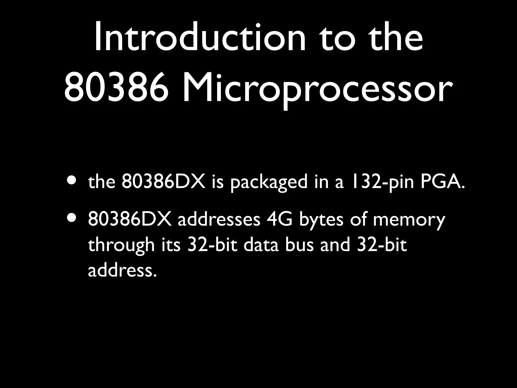
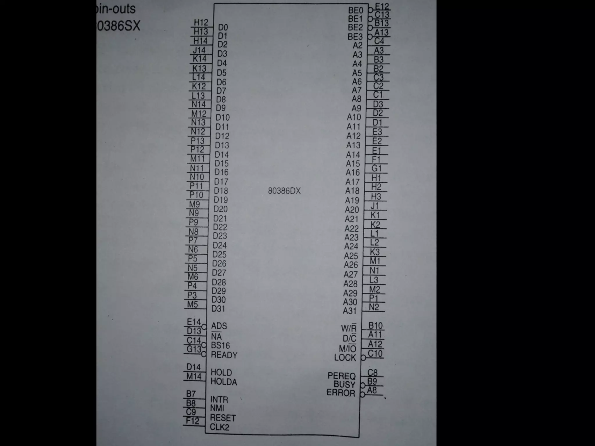
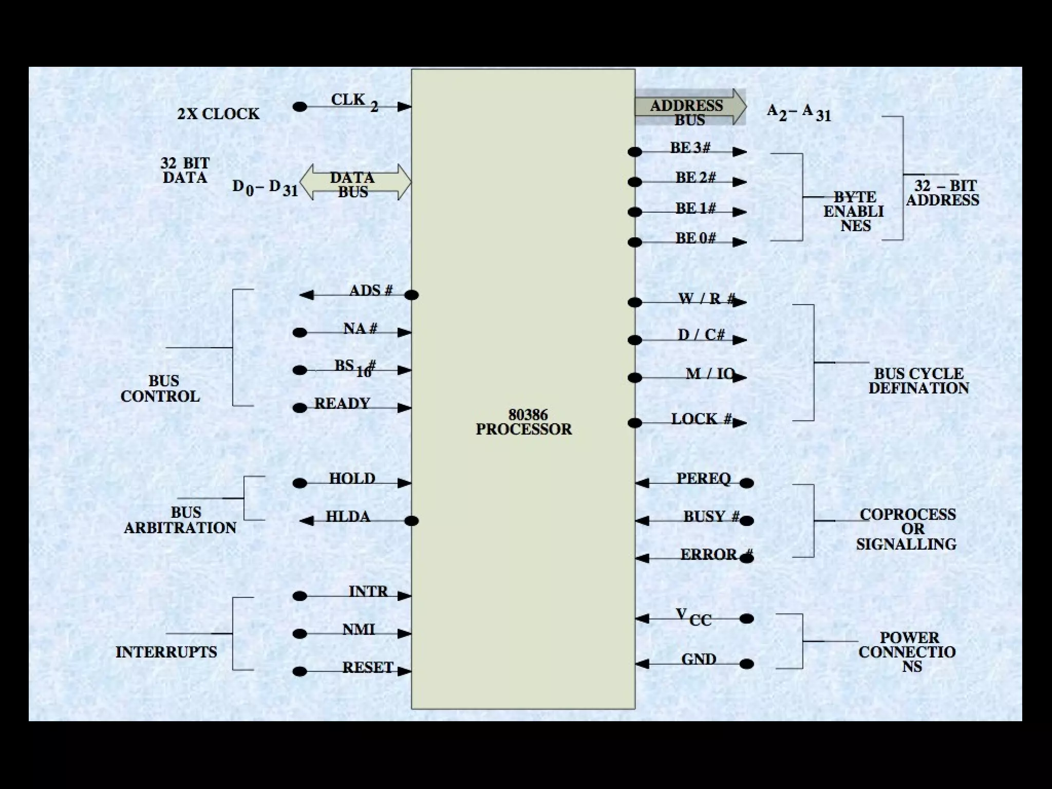
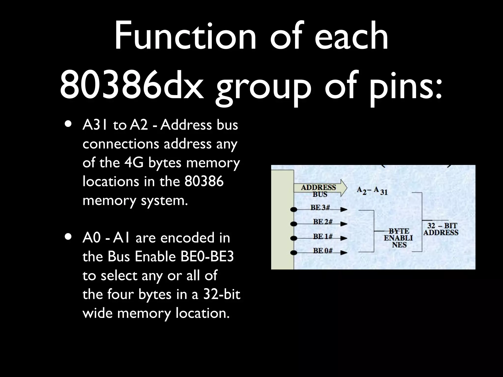
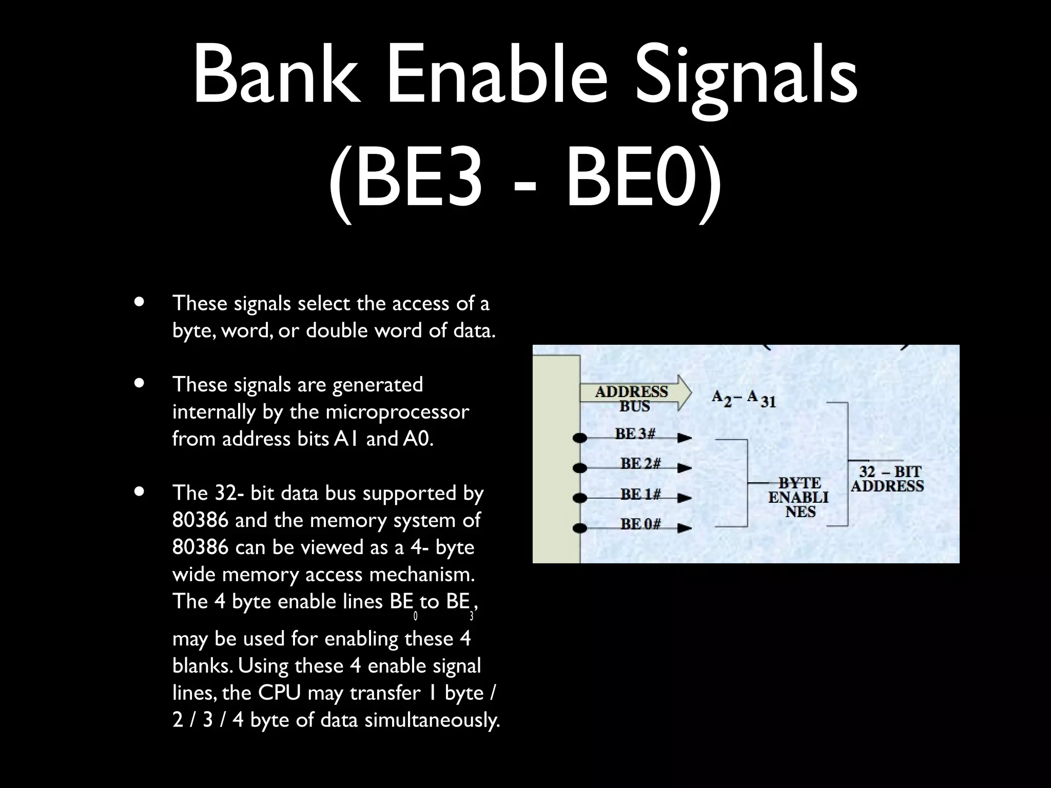
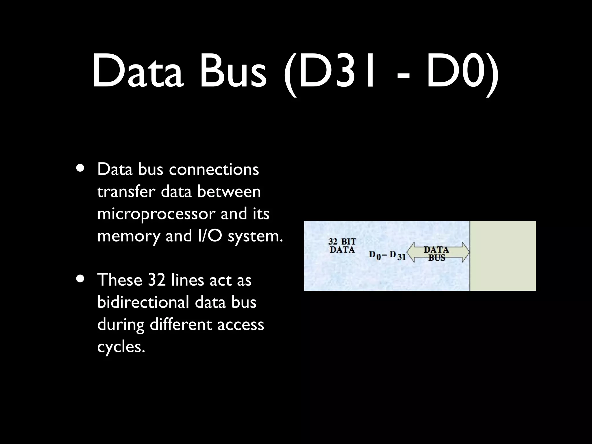


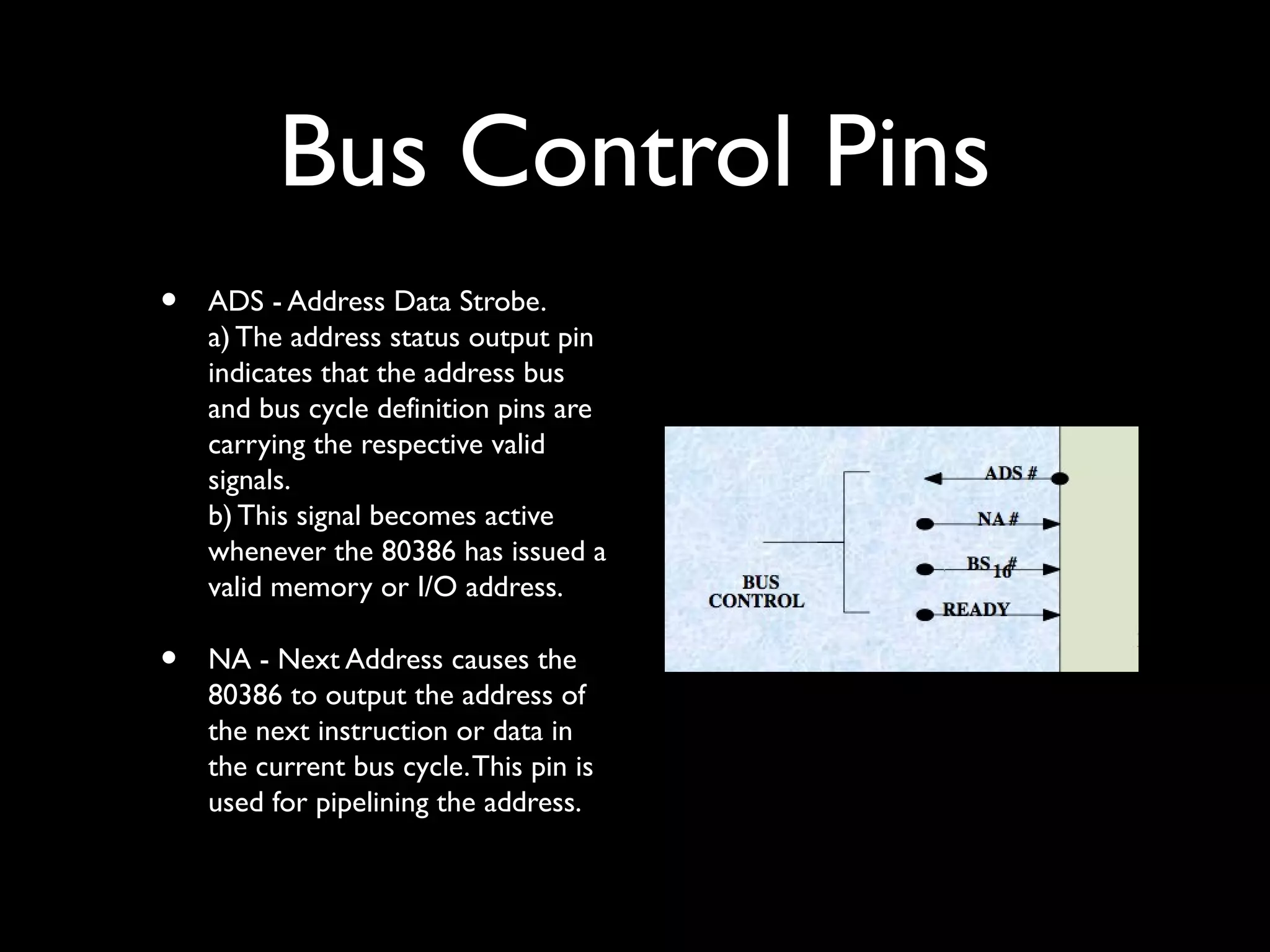

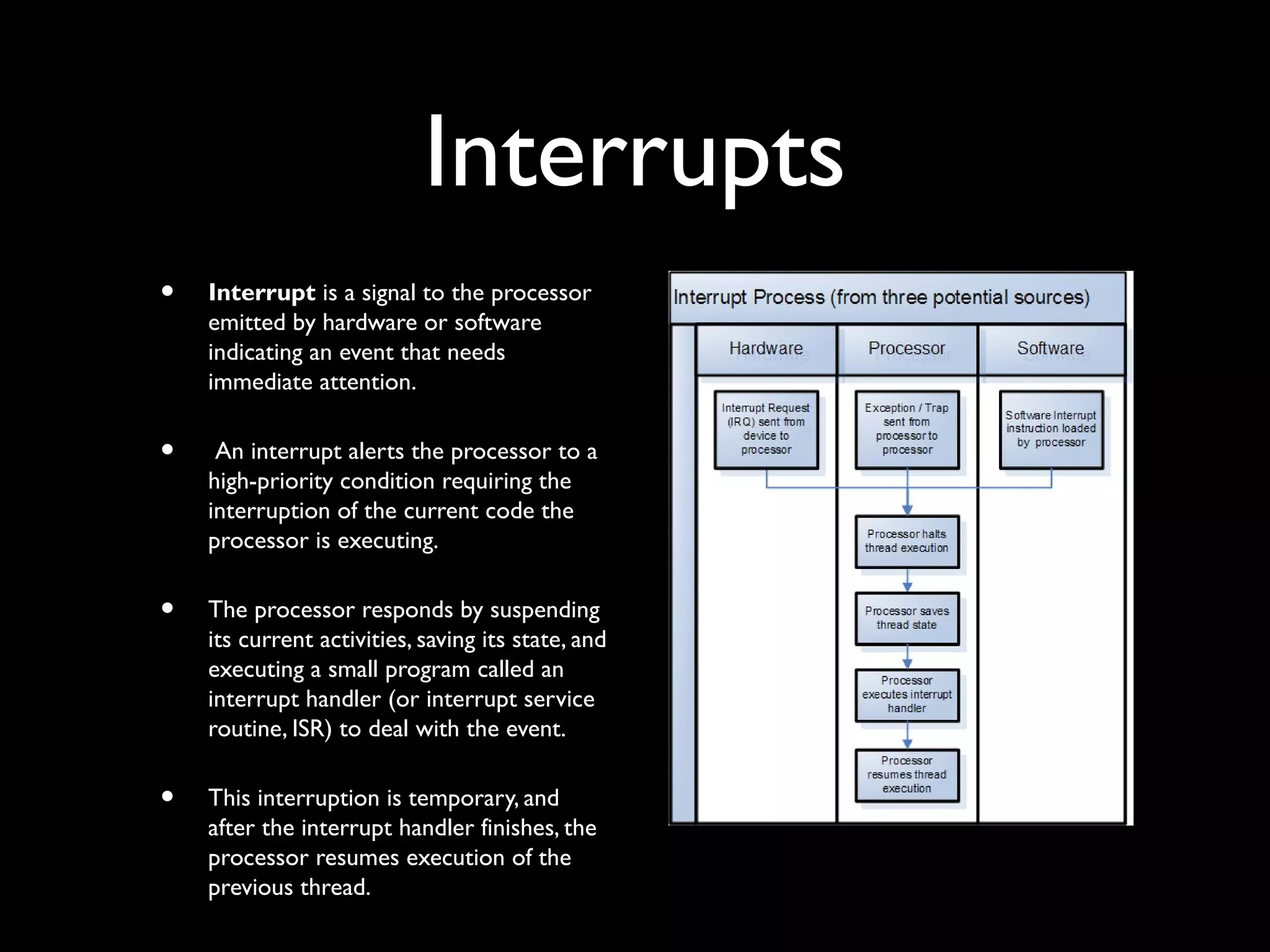
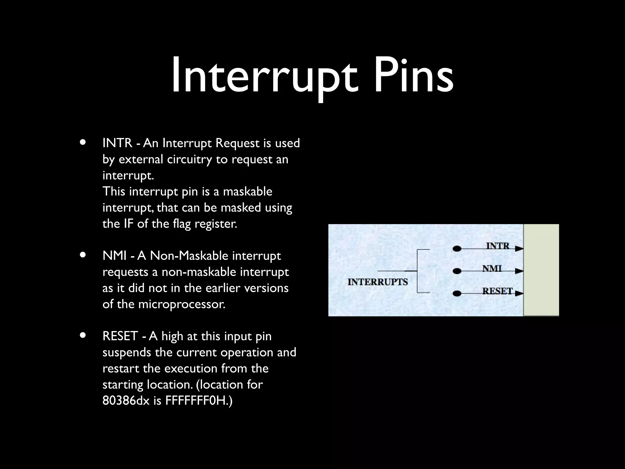

The document provides a detailed description of the 80386dx microprocessor, highlighting its architecture, pin functions, and various control signals. It explains how the microprocessor manages memory addresses, data transfers, and interrupt handling through its pin configurations. Additionally, it covers aspects such as bus arbitration, co-processor signaling, and clock timing relevant to the operation of the 80386dx.