Recommended

Recommended
More Related Content
What's hot
What's hot (19)
Similar to 1590591032374
Similar to 1590591032374 (20)
Recently uploaded
Recently uploaded (20)
1590591032374
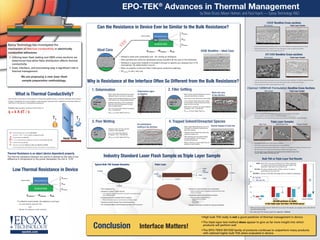
- 1. • Adhesive wets both substrates well. No voiding at interfaces. • Filler particles are uniformly distributed across bondline all the way to the interfaces. • Adhesion is good and material is complaint enough to absorb any stresses from CTE mismatches. No delamination occurs. • Resin is properly cured and fillers make good conductive pathway. • 2Rinterface is very, very low. • In both the bulk and triple layer samples, there is very uniform distribution of Ag flake throughout the sample. • Triple layer sample shows no evidence of air voids, delamination or resin–rich layers at the interface. • It is not surprising that ThRes in device reflects the bulk ThK. • In both the bulk and triple layer samples, there is very dense and uniform distribution of Ag flake throughout the sample. • Triple layer sample shows no evidence of air voids, delamination or resin–rich layers at the interface. • It is not surprising that ThRes in device reflects the bulk ThK. • In both the bulk and triple layer samples, the conductive filler does appear to have sintered. • Sintering appears to be more complete in the triple layer sample. • There appears to be only a very low level of resin binder remaining in either the bulk or triple layer sample. • The triple layer samples show a wide variety of conditions. • Some areas showed close to ideal bondlines with very good interfaces. • Other sections showed large areas of delamination – possibly from shrinkage due to sintering and solvent removal. • Still other portions of the sample showed huge areas consistent with trapped solvent. • The areas with air gaps, delamination and trapped solvent are likely the cause of the very poor ThRes results in the triple layer test. • Many highly filled adhesives have poor adhesion due to low resin component. • Highly solvent-loaded systems can shrink a lot during cure, causing delamination. • Stresses caused by CTE mismatches between Die and Substrate may also lead to delamination. • Air is one of the best thermal insulators: ThK = 0.024W/mK. • 2Rinterface is much higher than Rbulk • Many highly Ag filled adhesives use low viscosity resins/lots of solvent. • Ag is much more dense than resin base. • Low viscosity bases allow Ag to settle to the bottom of the bondline and resin base to rise to the top. • Base resin is another very good thermal insulators: ThK = 0.35W/mK. • Rinterface is much higher than Rbulk • Many highly filled adhesives use a lot of solvent or diluents to achieve the high filler loading. • Trapped solvent plasticizes resin and prevents proper cure. • Filler particles are not pulled closely enough together to form a good conductive pathway. • Rbulk in device is much higher than for properly cured material. • Adhesive does not fully wet the surface of the substrate. • Air is one of the best thermal insulators: ThK = 0.024W/mK. • 2Rinterface is much higher than Rbulk • Only measures Rbulk • Sample is cured in open format: • Low molecular weight components & solvents can escape during cure, inflating results. • Surfaces are often sanded flat for testing: • Resin-rich surface layers may be removed, inflating results. • Sample is much thicker than most bondlines. • No interfacial effects (Rinterface) are taken into account. • Sample is cured between two substrates. • Better simulates level of unreacted components that would remain in bondline. • Substrates define the bondline surface. • Better simulates interfacial effects: • Settling (resin-rich interface) • Voiding • Poor wetting • Delamination • Sample thickness is similar to typical bondlines. For effective heat transfer, the adhesive must have: • Low bulk resistivity (high bulk ThK) AND • Maintain low resistance at both interfaces Ideal Case 3. Poor Wetting 15-20mils 12.43mm 12.43mm 12.43mm 0.80mm 0.80mm ~5mils H20E or EK1000 Copper Copper 2. Filler Settling Ideal Area Typical Bulk ThK Sample Geometry Triple Layer Delaminated Area Triple Layer Samples Trapped Solvent 4. Trapped Solvent/Unreacted Species Delaminated region at interface Air pockets/poor wetting at top interface Resin-rich area at top interface Solvent trapped in bond line H20E Bondline – Ideal Case De-bonded areas Resin-rich layer Air voids Ideal Bondline Epoxy Technology has investigated the mechanism of thermal conductivity in electrically conductive adhesives. • Utilizing laser flash testing and SEM cross sections we determined how silver flake distribution effects thermal conductivity. • Cure, interface, and processing play a significant role in thermal management. We are proposing a new laser flash sample preparation methodology. What is Thermal Conductivity? • Heat transfer (conduction) will take place if a temperature gradient exists in a solid (or stationary fluid) medium. • Energy is transferred from more energetic to less energetic molecules when neighboring molecules collide (i.e. heat flows in the direction of decreasing temperature). Fourier’s Law expresses conductive heat transfer as q = k A dT / s Thermal Resistance is an object (device dependent) property. The thermal resistance between two points is defined as the ratio of the difference in temperature to the power dissipated; the unit is °C/W T1 T2 s A r e a Heat flow Low Thermal Resistance in Device Industry Standard Laser Flash Sample vs Triple Layer Sample H20E Bondline Cross-sections EK1000 Bondline Cross-sections Claimed 140W/mK Formulation Bondline Cross-Sections EPO-TEK® Advances in Thermal Management Bulk Sample Triple Layer Sample Ideal Bondline Bulk Sample Triple Layer Sample Bulk Sample Triple Layer Sample Semiconductor Substrate Adhesive Bondline interface R R R bulk interface Can the Resistance in Device Ever be Similar to the Bulk Resistance? Why is Resistance at the Interface Often So Different from the Bulk Resistance? 1. Delamination + = adhesive R bulk R interface 2R Semiconductor Substrate Adhesive Bondline interface R R R bulk interface + = adhesive R bulk R interface 2R q = heat transferred per unit time (W, Btu/hr) • remember 1 Watt= 1 Joule/sec (power= energy/unit of time) A = heat transfer area (m2, ft2) dT = T1-T2, the temperature difference across the material (K or oC, oF) s = material thickness (m, ft) k = thermal conductivity (W/m.K or W/m oC, Btu/(hr oF ft2/ft)) • A bulk material property that determines the rate of heat transfer for a given geometry by Brian Bruce, Mavyn Holman, and Paul Huynh — Epoxy Technology R&D epotek.com Bulk ThK vs Triple Layer Test Results EK1000 performs 3x better in the triple layer test then 140 W/mK epoxy! • High bulk ThK really is not a good predictor of thermal management in device • The triple layer test method does appear to give us far more insight into which products will perform well • The EPO-TEK® EK1000 family of products continues to outperform many products with claimed higher bulk ThK when evaluated in device H20E: Bulk ThK is only around 2W/mK but ThRes measured in customer devices has traditionally been better than expected. Triple layer test confirms this. EK1000: Routinely exhibits similar ThRes in device to what is expected from the bulk ThK. EK1000-1: Version of EK1000 with longer dry out. Great for processing. H20E 0 10 20 ThK (W/mK) 30 40 50 60 Bulk ThK Triple Layer ThK EK1000-1 3X EK1000 Claimed 140 W/mK • While we did not obtain the full 140W/mK for our bulk ThK results, our average value of 63.3W/mK was still extremely high. • But, triple layer ThK results ranged from only 4.8 – 7.5W/mK Y E S ! Conclusion Interface Matters!