1. Verilog Implementation of 16 bit Microprocessor - SAYEH
Manali R. Shah| Pooja Chaudhary | Prof. P. Uma Sathyakam | SELECT
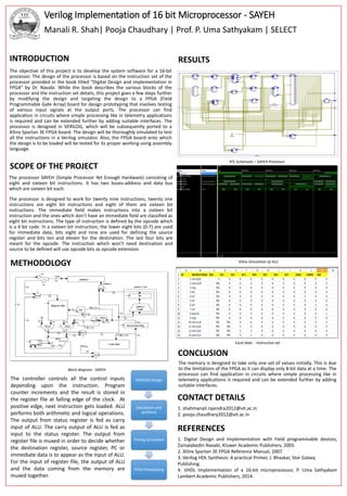
RTL Schematic – SAYEH Processor
Xilinx Simulation of ALU
Excel data - Instruction set
SCOPE OF THE PROJECT
RESULTS
METHODOLOGY
The processor SAYEH (Simple Processor Yet Enough Hardware) consisting of
eight and sixteen bit instructions. It has two buses-address and data bus
which are sixteen bit each.
The processor is designed to work for twenty nine instructions, twenty one
instructions are eight bit instructions and eight of them are sixteen bit
instructions. The immediate field makes instructions into a sixteen bit
instruction and the ones which don’t have an immediate field are classified as
eight bit instructions. The type of instruction is defined by the opcode which
is a 4 bit code. In a sixteen bit instruction, the lower eight bits (0-7) are used
for immediate data, bits eight and nine are used for defining the source
register and bits ten and eleven for the destination. The last four bits are
meant for the opcode. The instruction which won’t need destination and
source to be defined will use opcode bits as opcode extension.
The objective of this project is to develop the system software for a 16-bit
processor. The design of the processor is based on the instruction set of the
processor provided in the book titled “Digital Design and implementation in
FPGA” by Dr. Navabi. While the book describes the various blocks of the
processor and the instruction set details, this project goes a few steps further
by modifying the design and targeting the design to a FPGA (Field
Programmable Gate Array) board for design prototyping that involves testing
of various input signals at the output ports. The processor can find
application in circuits where simple processing like in telemetry applications
is required and can be extended further by adding suitable interfaces. The
processor is designed in VERILOG, which will be subsequently ported to a
Xilinx Spartan 3E FPGA board. The design will be thoroughly simulated to test
all the instructions in a Verilog simulator. Also, the FPGA board onto which
the design is to be loaded will be tested for its proper working using assembly
language.
INTRODUCTION
The memory is designed to take only one set of values initially. This is due
to the limitations of the FPGA as it can display only 8-bit data at a time. The
processor can find application in circuits where simple processing like in
telemetry applications is required and can be extended further by adding
suitable interfaces.
REFERENCES
1. Digital Design and Implementation with Field programmable devices,
Zainalabedin Navabi, Kluwer Academic Publishers, 2005.
2. Xilinx Spartan 3E FPGA Reference Manual, 2007.
3. Verilog HDL Synthesis: A practical Primer, J. Bhaskar, Star Galaxy
Publishing.
4. VHDL Implementation of a 16-bit microprocessor, P. Uma Sathyakam
Lambert Academic Publishers, 2014.
CONTACT DETAILS
1. shahmanali.rajendra2012@vit.ac.in
2. pooja.chaudhary2012@vit.ac.in
VERILOG Design
Simulation and
synthesis
Timing Simulation
FPGA Prototyping
Block diagram - SAYEH
The controller controls all the control inputs
depending upon the instruction. Program
counter increments and the result is stored in
the register file at falling edge of the clock. At
positive edge, next instruction gets loaded. ALU
performs both arithmetic and logical operations.
The output from status register is fed as carry
input of ALU. The carry output of ALU is fed as
input to the status register. The output from
register file is muxed in order to decide whether
the destination register, source register, PC or
immediate data is to appear as the input of ALU.
For the input of register file, the output of ALU
and the data coming from the memory are
muxed together.
CONCLUSION