
Recommended
More Related Content
What's hot
What's hot (20)
Similar to Substrate / wafers and Basic concepts Of Mems & microsystems
Similar to Substrate / wafers and Basic concepts Of Mems & microsystems (20)
Recently uploaded
Recently uploaded (20)
Substrate / wafers and Basic concepts Of Mems & microsystems
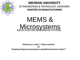
- 1. MEHRAN UNIVERSITY OF ENGINEERING & TECHNOLOGY, JAMSHORO MASTERS IN MANUFACTURING MEHRAN UNIVERSITY OF ENGINEERING & TECHNOLOGY, JAMSHORO MASTERS IN MANUFACTURING MEMS & MicrosystemsMICRO-ELECTRO-MECHANICAL SYSTEMS ”Machine on a chip” / “Micro-machine” Or ”Anything designed and produced using Microelectronics toolset ”
- 2. MEHRAN UNIVERSITY OF ENGINEERING & TECHNOLOGY, JAMSHORO MASTERS IN MANUFACTURING MEHRAN UNIVERSITY OF ENGINEERING & TECHNOLOGY, JAMSHORO MASTERS IN MANUFACTURING MEMS & Microsystems MICRO-ELECTRO-MECHANICAL SYSTEMS
- 3. MEHRAN UNIVERSITY OF ENGINEERING & TECHNOLOGY, JAMSHORO MASTERS IN MANUFACTURING MEHRAN UNIVERSITY OF ENGINEERING & TECHNOLOGY, JAMSHORO MASTERS IN MANUFACTURING Contents: • Substrate or Wafers • Substrate Materials • Silicon as a Substrate Material • Miller Indices • Mechanical properties of Silicon • Silicon Compounds
- 4. MEHRAN UNIVERSITY OF ENGINEERING & TECHNOLOGY, JAMSHORO MASTERS IN MANUFACTURING MEHRAN UNIVERSITY OF ENGINEERING & TECHNOLOGY, JAMSHORO MASTERS IN MANUFACTURING Wafers • A wafer, also called a slice, is a thin slice of semiconductor material, such as a crystalline silicon, used in electronics for the fabrication of integrated circuits and in photovoltaics for conventional, wafer-based solar cells. • The wafer serves as the layer for microelectronic devices built in and over the wafer and undergoes many microfabrication process steps such as doping of ion implantation, etching, deposition of various materials, and photolithographic patterning. • Finally the individual microcircuits are separated (dicing) and packaged.
- 5. MEHRAN UNIVERSITY OF ENGINEERING & TECHNOLOGY, JAMSHORO MASTERS IN MANUFACTURING MEHRAN UNIVERSITY OF ENGINEERING & TECHNOLOGY, JAMSHORO MASTERS IN MANUFACTURING Wafers • Wafer is a solid substance onto which a layer of another substance is applied, and to which that second substance adheres. • In solid-state electronics, this term refers to a thin slice of material such as silicon, silicon dioxide, aluminum oxide, sapphire, germanium, gallium arsenide (GaAs), an alloy of silicon and germanium, or indium phosphide (InP). • These serve as the foundation upon which electronic devices such as transistors, diodes, and especially integrated circuits (ICs) are deposited.
- 6. MEHRAN UNIVERSITY OF ENGINEERING & TECHNOLOGY, JAMSHORO MASTERS IN MANUFACTURING MEHRAN UNIVERSITY OF ENGINEERING & TECHNOLOGY, JAMSHORO MASTERS IN MANUFACTURING Wafer • Wafers are formed of highly pure (99.9999999% purity), nearly defect-free single crystalline material. • The wafer is a slice cut from a larger piece of a single crystal substrate. Wafers can be of silicon or other single crystalline material such as quartz or gallium arsenide. • A single crystal is a material in which the crystal lattice of the entire sample is continuous and unbroken.
- 7. MEHRAN UNIVERSITY OF ENGINEERING & TECHNOLOGY, JAMSHORO MASTERS IN MANUFACTURING MEHRAN UNIVERSITY OF ENGINEERING & TECHNOLOGY, JAMSHORO MASTERS IN MANUFACTURING Wafer & Substrate • In microelectronics, the wafer means a flat macroscopic object on which micro-fabrication processes take place. • In microsystems, a substrate serves an additional purpose: it acts as signal transducer besides supporting other transducers that convert mechanical actions to electrical outputs or vice versa.
- 8. MEHRAN UNIVERSITY OF ENGINEERING & TECHNOLOGY, JAMSHORO MASTERS IN MANUFACTURING MEHRAN UNIVERSITY OF ENGINEERING & TECHNOLOGY, JAMSHORO MASTERS IN MANUFACTURING Substrates / Wafers Materials The common substrate materials used in MEMS are silicon (Si), germanium (Ge), and gallium arsenide (GaAs) all fall in the category of semiconductors. One major reason for using these materials as principal substrate materials in both microelectronics and microsystems is that these materials are at the borderline between conductors and insulators, so they can be made either a conductor or an insulator as needs arise. The doping techniques can be used to convert the most commonly used semiconducting material to an electrically conducting material by doping it with a foreign material for conducting electricity.
- 9. MEHRAN UNIVERSITY OF ENGINEERING & TECHNOLOGY, JAMSHORO MASTERS IN MANUFACTURING MEHRAN UNIVERSITY OF ENGINEERING & TECHNOLOGY, JAMSHORO MASTERS IN MANUFACTURING Substrate Material substrate materials for microsystems with typical electrical resistivity of conductors, semiconductors and insulators are shown below:
- 10. MEHRAN UNIVERSITY OF ENGINEERING & TECHNOLOGY, JAMSHORO MASTERS IN MANUFACTURING MEHRAN UNIVERSITY OF ENGINEERING & TECHNOLOGY, JAMSHORO MASTERS IN MANUFACTURING Substrate / wafer Material There are two types of substrate materials used in microsystems: 1- Passive substrate materials 2- Active substrate materials The passive material is one that does not play an essential role in the sensing mechanism. Passive materials are only used to provide either mechanical structure or electrical connection.
- 11. MEHRAN UNIVERSITY OF ENGINEERING & TECHNOLOGY, JAMSHORO MASTERS IN MANUFACTURING MEHRAN UNIVERSITY OF ENGINEERING & TECHNOLOGY, JAMSHORO MASTERS IN MANUFACTURING Active Substrate Materials • Active substrate materials are primarily used for sensors and actuators in a microsystems and in other MEMS components. • Typical active substrate materials for microsystems include silicon, gallium arsenide, germanium, and quartz. Silicon
- 12. MEHRAN UNIVERSITY OF ENGINEERING & TECHNOLOGY, JAMSHORO MASTERS IN MANUFACTURING MEHRAN UNIVERSITY OF ENGINEERING & TECHNOLOGY, JAMSHORO MASTERS IN MANUFACTURING Active Substrate Materials • These substrate materials have basically a cubic crystal lattice with a tetrahedral atomic bond. • These materials are selected as active substrates primarily for their dimensional stability, which is relatively insensitive to environmental conditions. Silicon
- 13. MEHRAN UNIVERSITY OF ENGINEERING & TECHNOLOGY, JAMSHORO MASTERS IN MANUFACTURING MEHRAN UNIVERSITY OF ENGINEERING & TECHNOLOGY, JAMSHORO MASTERS IN MANUFACTURING Active Substrate Materials • Dimensional stability is a critical requirement for sensors and actuators with high precision Silicon
- 14. MEHRAN UNIVERSITY OF ENGINEERING & TECHNOLOGY, JAMSHORO MASTERS IN MANUFACTURING MEHRAN UNIVERSITY OF ENGINEERING & TECHNOLOGY, JAMSHORO MASTERS IN MANUFACTURING Silicon as a Substrate Material Silicon is the most widely used substrate material for MEMS and microsystems. The popularity of silicon for such application is primarily for the following reasons: 1. It is mechanically stable and it can be integrated into electronics on the same substrate. 2. Electronics for signal transduction, such as a p- or n-type piezoresistor, can be readily integrated with the Si substrate. 3. Silicon is almost an ideal structural material. It has about the same Young’s modulus as steel (about 2 x 10⁵ MPa), but is as light as aluminum, with a mass density of about 2.3 g/cm3 . Materials with a high Young’s modulus can better maintain a linear relationship between applied load and the induced deformations.
- 15. MEHRAN UNIVERSITY OF ENGINEERING & TECHNOLOGY, JAMSHORO MASTERS IN MANUFACTURING MEHRAN UNIVERSITY OF ENGINEERING & TECHNOLOGY, JAMSHORO MASTERS IN MANUFACTURING Silicon as a Substrate Material 4. It has a melting point at 1400°C, which is about twice as high as that of aluminum. This high melting point makes silicon dimensionally stable even at elevated temperature. 5. Its thermal expansion coefficient is about 8 times smaller than that of steel, and is more than 10 times smaller than that of aluminum. It is thus an ideal candidate material for sensors and actuators. The silicon wafers are extremely flat and accept coatings and additional thin- film layers for building micro-structural geometry or conducting electricity.
- 16. MEHRAN UNIVERSITY OF ENGINEERING & TECHNOLOGY, JAMSHORO MASTERS IN MANUFACTURING MEHRAN UNIVERSITY OF ENGINEERING & TECHNOLOGY, JAMSHORO MASTERS IN MANUFACTURING Miller Indices Miller indices form a notation system in crystallography for planes in crystal lattices. The family of lattice planes is determined by three integers h, k, and ℓ, the Miller indices. Crystallography is the experimental science of determining the arrangement of atoms in the crystalline solids.
- 17. MEHRAN UNIVERSITY OF ENGINEERING & TECHNOLOGY, JAMSHORO MASTERS IN MANUFACTURING MEHRAN UNIVERSITY OF ENGINEERING & TECHNOLOGY, JAMSHORO MASTERS IN MANUFACTURING Miller Indices It is often necessary to be able to specify certain directions and planes in crystals. Many material properties and machining processes vary with direction in the crystal. The strength of material also vary with direction in the crystal. The wafers that are shipped by suppliers normally indicate in which directions, the cuts have been made to make flat surface. Directions and planes are described using three integers Miller Indices. Miller index is denoted by (hkl).
- 18. MEHRAN UNIVERSITY OF ENGINEERING & TECHNOLOGY, JAMSHORO MASTERS IN MANUFACTURING MEHRAN UNIVERSITY OF ENGINEERING & TECHNOLOGY, JAMSHORO MASTERS IN MANUFACTURING Miller Indices STEP-2 Specify the intercepts in fractional co-ordinates Fractional Intercepts : a/a , ∞/a, ∞/a i.e. 1 , ∞ , ∞ STEP-1 Identify the intercepts on the x- , y- and z- axes. It intercepts on the x- axes at point a. The surface is parallel to the y- and z-axes. Therefore, intercepts on both axes is ∞. The point is (x,y,z)=(a, ∞, ∞) STEP-3 Take the reciprocals of the fractional intercepts Reciprocals : 1/1 , ∞/1, ∞/1 i.e. 1 , 0 , 0 Therefore: Miller Indices : (100)
- 19. MEHRAN UNIVERSITY OF ENGINEERING & TECHNOLOGY, JAMSHORO MASTERS IN MANUFACTURING MEHRAN UNIVERSITY OF ENGINEERING & TECHNOLOGY, JAMSHORO MASTERS IN MANUFACTURING Miller Index
- 20. MEHRAN UNIVERSITY OF ENGINEERING & TECHNOLOGY, JAMSHORO MASTERS IN MANUFACTURING MEHRAN UNIVERSITY OF ENGINEERING & TECHNOLOGY, JAMSHORO MASTERS IN MANUFACTURING Miller Indices
- 21. MEHRAN UNIVERSITY OF ENGINEERING & TECHNOLOGY, JAMSHORO MASTERS IN MANUFACTURING MEHRAN UNIVERSITY OF ENGINEERING & TECHNOLOGY, JAMSHORO MASTERS IN MANUFACTURING Miller Indices On <111> plane, the lattice distances between adjacent atoms are shortest. These short lattice distances between atoms make the attractive forces between atoms stronger on this plane than those on the other two planes. Also, this plane contains three of the four atoms that are situated at the center of the faces of the unit cell. Thus, the growth of crystal in this plane is the slowest and the fabrication processes, e.g., etching, as we will learn will proceed slowest.
- 22. MEHRAN UNIVERSITY OF ENGINEERING & TECHNOLOGY, JAMSHORO MASTERS IN MANUFACTURING MEHRAN UNIVERSITY OF ENGINEERING & TECHNOLOGY, JAMSHORO MASTERS IN MANUFACTURING Miller Indices
- 23. MEHRAN UNIVERSITY OF ENGINEERING & TECHNOLOGY, JAMSHORO MASTERS IN MANUFACTURING MEHRAN UNIVERSITY OF ENGINEERING & TECHNOLOGY, JAMSHORO MASTERS IN MANUFACTURING TASK # 1 Search publication on following topic. MICRO MANUFACTURING Read Abstract and Conclusion Write a summary of minimum two pages and reply the following queries. WHAT, WHY, WHERE, WHO, WHOM, and HOW
- 24. MEHRAN UNIVERSITY OF ENGINEERING & TECHNOLOGY, JAMSHORO MASTERS IN MANUFACTURING MEHRAN UNIVERSITY OF ENGINEERING & TECHNOLOGY, JAMSHORO MASTERS IN MANUFACTURING Mechanical Properties of Silicon • It is a prime material in MEMS microsystems for sensors and actuators. • Its three dimensional geometry withstand often severe mechanical and thermal loads, and accommodating electrical instruments such as piezoresistive integrated into it. • Silicon is an elastic material with no plasticity or creep below 800°C. • It shows virtually no fatigue failure under all conceivable circumstances. • These unique characteristics make it an ideal material for sensing and actuating in MEMS microsystems.
- 25. MEHRAN UNIVERSITY OF ENGINEERING & TECHNOLOGY, JAMSHORO MASTERS IN MANUFACTURING MEHRAN UNIVERSITY OF ENGINEERING & TECHNOLOGY, JAMSHORO MASTERS IN MANUFACTURING Mechanical Properties of Silicon • It is a brittle material. Therefore, undesirable brittle fracture behavior with weak resistance to impact loads needs to be considered in the design of such microsystems. • It is anisotropic, this makes accurate stress analysis of silicon structures tedious, since directional mechanical property must be included. .
- 26. MEHRAN UNIVERSITY OF ENGINEERING & TECHNOLOGY, JAMSHORO MASTERS IN MANUFACTURING MEHRAN UNIVERSITY OF ENGINEERING & TECHNOLOGY, JAMSHORO MASTERS IN MANUFACTURING Mechanical Properties of Silicon • For most cases in microsystem design, the bulk material properties of silicon, silicon compounds, and other active substrate materials presented in table are used.
- 27. MEHRAN UNIVERSITY OF ENGINEERING & TECHNOLOGY, JAMSHORO MASTERS IN MANUFACTURING MEHRAN UNIVERSITY OF ENGINEERING & TECHNOLOGY, JAMSHORO MASTERS IN MANUFACTURING Mechanical Properties of Silicon • It can be observed from table that copper has the highest thermal diffusivity, whereas, silicon and aluminum have about the same value. • The silicon oxide conducts heat more than 150 times slower than silicon and aluminum. It observed that copper films are the best material for fast heat transmission in microsystems, whereas silicon dioxide can be used as an effective thermal barrier.
- 28. MEHRAN UNIVERSITY OF ENGINEERING & TECHNOLOGY, JAMSHORO MASTERS IN MANUFACTURING MEHRAN UNIVERSITY OF ENGINEERING & TECHNOLOGY, JAMSHORO MASTERS IN MANUFACTURING Silicon Compounds Following three silicon compounds are often used in microsystems: SiO2 Silicon dioxide SiC Silicon Carbide Si3N4 Silicon Nitride
- 29. MEHRAN UNIVERSITY OF ENGINEERING & TECHNOLOGY, JAMSHORO MASTERS IN MANUFACTURING MEHRAN UNIVERSITY OF ENGINEERING & TECHNOLOGY, JAMSHORO MASTERS IN MANUFACTURING Silicon Compounds There are three principal uses of silicon oxide in microsystems: (1) as a thermal and electric insulator. (2) as a mask in the etching of silicon substrates. and (3) as a sacrificial layer in surface micromachining. Silicon oxide has much stronger resistance to most etchants than silicon. Silicon Oxide (SiO2)
- 30. MEHRAN UNIVERSITY OF ENGINEERING & TECHNOLOGY, JAMSHORO MASTERS IN MANUFACTURING MEHRAN UNIVERSITY OF ENGINEERING & TECHNOLOGY, JAMSHORO MASTERS IN MANUFACTURING Silicon Compounds Silicon dioxide can be produced by heating silicon in an oxidant such as oxygen with or without steam. Chemical reactions for such processes are: Dry Oxidation (without steam): Wet Oxidation (with steam): The process can be accelerated to much faster rates by the presence of steam; the highly activated H2O molecules enhance the process. Silicon Oxide (SiO2)
- 31. MEHRAN UNIVERSITY OF ENGINEERING & TECHNOLOGY, JAMSHORO MASTERS IN MANUFACTURING MEHRAN UNIVERSITY OF ENGINEERING & TECHNOLOGY, JAMSHORO MASTERS IN MANUFACTURING Silicon Compounds Silicon Oxide (SiO2) The team created silicon dioxide (SiO2) nanotube anodes for lithium-ion batteries and found they had over three times as much energy storage capacity as the carbon-based anodes currently being used. This has significant implications for industries including electronics and electric vehicles, which are always trying to squeeze longer discharges out of batteries.
- 32. MEHRAN UNIVERSITY OF ENGINEERING & TECHNOLOGY, JAMSHORO MASTERS IN MANUFACTURING MEHRAN UNIVERSITY OF ENGINEERING & TECHNOLOGY, JAMSHORO MASTERS IN MANUFACTURING Silicon Compounds The principal applications of silicon carbide (SiC) in microsystems are: (1) its dimensional and chemical stability at high temperatures. (2) It has very strong resistance to oxidation even at very high temperatures. (3) Thin films of silicon carbide are often deposited over MEMS components to protect them from extreme temperature. (4) Using SiC in MEMS is that dry etching with aluminum masks can easily pattern the thin SiC film. The patterned SiC film can further be used as a protective layer in micromachining for the underlying silicon substrate, as SiC can resist common etchants Silicon exists in the raw materials of carbon (coal, coke, wood chips, etc.), the intense heating of these materials in the electric arc furnace results in SiC sinking to the bottom of the crucible. Silicon Carbide (SiC)
- 33. MEHRAN UNIVERSITY OF ENGINEERING & TECHNOLOGY, JAMSHORO MASTERS IN MANUFACTURING MEHRAN UNIVERSITY OF ENGINEERING & TECHNOLOGY, JAMSHORO MASTERS IN MANUFACTURING Silicon Compounds (1) It provides an excellent barrier to diffusion of water and ions such as sodium. (2) Its ultra strong resistance to oxidation and many etchants makes it suitable for masks for deep etching. (3) Applications of silicon nitride include optical waveguides, encapsulation to prevent diffusion of water and other toxic fluids into the substrate. (4) It is also used as high-strength electric insulators and ion implantation masks. Silicon nitride can be produced from silicon-containing gases and NH3 in the following reaction: Silicon Nitride(Si3N4)
- 34. MEHRAN UNIVERSITY OF ENGINEERING & TECHNOLOGY, JAMSHORO MASTERS IN MANUFACTURING MEHRAN UNIVERSITY OF ENGINEERING & TECHNOLOGY, JAMSHORO MASTERS IN MANUFACTURING Silicon Compounds Silicon in polycrystalline form can be deposited onto silicon substrates by chemical vapor deposition (CVD). It is a principal material in surface micromachining. The low pressure chemical vapor deposition (LPCVD) process is frequently used for depositing polycrystalline silicon onto silicon substrates. The temperature involved in this process is about 600 to 650°C. Polycrystalline silicon is widely used in the IC industry for resistors, gates for transistors, thin-film transistors. Polycrystalline Silicon
- 35. MEHRAN UNIVERSITY OF ENGINEERING & TECHNOLOGY, JAMSHORO MASTERS IN MANUFACTURING MEHRAN UNIVERSITY OF ENGINEERING & TECHNOLOGY, JAMSHORO MASTERS IN MANUFACTURING Essay Questions • What is substrate / wafer? • Explain substrate’s materials? • Clarify the importance of silicon as substrate material? • Define Miller Index and its use in Crystallography with diagrams? • List the thermal diffusivities of silicon, silicon dioxide, aluminum, and copper, and make an observation on the results? • Explain the role of silicon dioxide (SiO2); silicon carbide (SiC); and silicon nitride (Si3N4) in MEMS microsystems. Fill in the blanks / MCQ Questions