- The document describes the design and testing of germanium ridge waveguide structures for 3.3 μm and 10 μm wavelength single-mode operation. Simulations were used to optimize the waveguide dimensions. Process verification using SEM showed issues with sidewall roughness and etching profile in amorphous germanium. X-ray diffraction confirmed the amorphous nature of germanium samples. Transmission measurements provided insight into coupling challenges in germanium due to its high refractive index. While transmission was observed in crystalline germanium waveguides, no transmission was measured in single-mode crystalline or amorphous germanium waveguides, likely due to processing or coupling challenges.
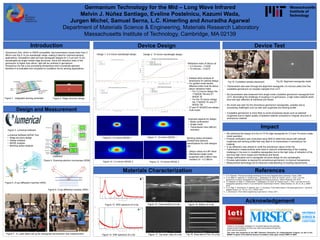
Germanium Technology for the Mid-Long Wave Infrared Poster
1. Germanium Technology for the Mid – Long Wave Infrared
Melvin J. Núñez Santiago, Eveline Postelnicu, Kazumi Wada,
Jurgen Michel, Samuel Serna, L.C. Kimerling and Anuradha Agarwal
Department of Materials Science & Engineering, Materials Research Laboratory
Massachusetts Institute of Technology, Cambridge, MA 02139
Introduction
Design and Measurement
Device Design
Figure 2. Ridge structure design
Refractive Index of Silicon at:
• 3.3 microns – 3.4335
• 10 microns – 3.4215
Figure 9. 3.3 micron MODE 1
Figure 10. 3.3 micron MODE 2
Figure 11. 10 micron MODE 1
Figure 12. 10 micron MODE 2
• Sweeps allow analysis of
dimensions for optimal design.
• For guided mode results,
effective index must be above
silicon refractive index:
• For 3.3 micron design the
1st MODE TM and 2nd
MODE TE
• For the 10 micron design
the 1st MODE TE and 2nd
MODE TM
• 3rd and 4th MODES are always
multi-mode.
Device Test
Impact
Materials Characterization
Acknowledgement
This work was supported by the MRL Research Experience for Undergraduates Program, as part of the
MRSEC Program of the National Science Foundation under grant number DMR-14-19807.
Important aspects for design:
• Mode confinement
• Single mode
• Transmission loss (dB/cm)
reduction
Figure 5. X-ray diffraction machine (XRD)
Figure 4. Scanning electron microscope (SEM)
Lumerical Software MODE Tool:
• Ridge structure design
• Sweep analysis
• MODE analysis
• Bending radius analysis
Bending radius simulation
showed that optimum
specifications for both designs
are:
• 200µm radius at a 90º bend
• Maintained single mode
properties with a dB/cm loss
variation of ~ 0.2 dB/cm
Germanium (Ge), which is CMOS-compatible, has transmission losses lower than 2
dB/cm over the 2-14 µm wavelength range, making it ideal for chemical sensing
applications. Simulations yield low-loss waveguide designs for 3.3 µm and 10 µm
wavelengths as single-moded ridge structures. Since the refractive index of the
germanium is higher than silicon, light will be confined in germanium.
Amorphous Ge has a low processing temperature and is substrate-agnostic;
therefore it is evaluated and compared to crystalline Ge for sensing applications.
Si
Ge
Figure 1. Integrated sensing schematic
References
Thanks to my principal investigator Dr. Anuradha Agarwal and graduate
student Eveline Postelnicu for their time, effort and guidance through this
entire learning experience
1. D. K. Sparacin, “Process and design techniques for low loss integrated silicon photonics,” thesis, 2006.
2. R. W. Millar, K. Gallacher, U. Griskeviciute, L. Baldassarre, M. Sorel, M. Ortolani, and D. J. Paul, “Low loss
germanium-on-silicon waveguides for integrated mid-infrared photonics,” Silicon Photonics XIV, 2019.
3. K. Gallacher, R. Millar, U. Griškevičiūte, L. Baldassarre, M. Sorel, M. Ortolani, and D. J. Paul, “Low loss Ge-on-Si
waveguides operating in the 8–14 µm atmospheric transmission window,” Optics Express, vol. 26, no. 20, p. 25667,
2018.
4. N. S. Patel, C. Monmeyran, A. Agarwal, and L. C. Kimerling, “Point defect states in Sb-doped germanium,” Journal of
Applied Physics, vol. 118, no. 15, p. 155702, 2015.
5. C. Monmeyran, “Point defect engineering in germanium,” thesis, 2017.
Figure 7 - 8. Laser beam set-up for waveguide transmission loss measurement
• We optimized the design of a Ge on FZ-Si ridge waveguide for 3.3 and 10-micron single
mode operation.
• Process verification was conducted using SEM to determine issues with sidewall
roughness and etching profile that may lead to no transmission in amorphous Ge
material.
• X ray diffraction was utilized to verify the amorphous nature of the Ge.
• Transmission measurements were used to improve understanding of the coupling
challenge in Ge even in crystalline waveguides due to the high index of refraction of Ge
and thus high mirror losses and interfaces and facets.
• Design optimization led to waveguide structure design for two wavelengths
• Process optimization is required for amorphous germanium, to improve transparency
• Measurement technology led to improved understanding of coupling requirements
• Transmission was seen through the alignment waveguide (10 microns wide) from the
crystalline germanium on insulator samples from LETI
• No transmission was measured form single mode crystalline germanium waveguide from
LETI, illuminating the challenge of coupling in to germanium, a high index material which
thus has high reflection at interfaces and facets
• No mode was seen for the amorphous germanium waveguides, possibly due to
processing challenges such as side wall roughness and etching profile
• Crystalline germanium is more likely to avoid processing issues such as sidewall
roughness due to higher quality of epitaxial material compared to irregular structure of
amorphous material.
Design 1: 3.3 micron wavelength design Design 2: 10 micron wavelength design
Figure 13. XRD spectrum of α-Ge
Figure 14. XRD spectrum of x-Ge Figure 17. Top down view of α-Ge Fig 18. Dose test of FOx-16 α-Ge
Figure 15. Cross section of α-Ge Figure 16. 920nm of α-Ge
Figure 3. Lumerical software
Figure 6. X-ray diffraction process (XRD)
Laser
Mirrors
Chopper
Mid-IR
camera
Sample
Microscope
Lens
Fig 19. Crystalline sample placement Fig 20. Alignment waveguide mode