
Recommended
More Related Content
What's hot
What's hot (15)
Similar to Silicon NPN Phototransistor Specs
Similar to Silicon NPN Phototransistor Specs (20)
More from MarioFarias18
More from MarioFarias18 (9)
Recently uploaded
Recently uploaded (20)
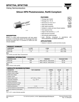
Silicon NPN Phototransistor Specs
- 1. Silicon NPN Phototransistor, RoHS Compliant www.vishay.com For technical questions, contact: detectortechsupport@vishay.com Document Number: 81527 402 Rev. 1.5, 08-Sep-08 BPW77NA, BPW77NB Vishay Semiconductors DESCRIPTION BPW77 is a silicon NPN phototransistor with high radiant sensitivity in hermetically sealed TO-18 package with base terminal and glass lens. It is sensitive to visible and near infrared radiation. FEATURES • Package type: leaded • Package form: TO-18 • Dimensions (in mm): Ø 4.7 • High photo sensitivity • High radiant sensitivity • Suitable for visible and near infrared radiation • Fast response times • Angle of half sensitivity: ϕ = ± 10° • Base terminal connected • Hermetically sealed package • Lead (Pb)-free component in accordance with RoHS 2002/95/EC and WEEE 2002/96/EC APPLICATIONS • Detector in electronic control and drive circuits Note Test condition see table “Basic Characteristics” Note MOQ: minimum order quantity Note Tamb = 25 °C, unless otherwise specified 94 8401 PRODUCT SUMMARY COMPONENT Ica (mA) ϕ (deg) λ0.1 (nm) BPW77NA 7.5 to 15 ± 10 450 to 1080 BPW77NB > 10 ± 10 450 to 1080 ORDERING INFORMATION ORDERING CODE PACKAGING REMARKS PACKAGE FORM BPW77NA Bulk MOQ: 1000 pcs, 1000 pcs/bulk TO-18 BPW77NB Bulk MOQ: 1000 pcs, 1000 pcs/bulk TO-18 ABSOLUTE MAXIMUM RATINGS PARAMETER TEST CONDITION SYMBOL VALUE UNIT Collector base voltage VCBO 80 V Collector emitter voltage VCEO 70 V Emitter base voltage VEBO 5 V Collector current IC 50 mA Collector peak current tp/T = 0.5, tp ≤ 10 ms ICM 100 mA Total power dissipation Tamb ≤ 25 °C PV 250 mW Junction temperature Tj 125 °C Operating temperature range Tamb - 40 to + 125 °C Storage temperature range Tstg - 40 to + 125 °C Soldering temperature t ≤ 5 s Tsd 260 °C Thermal resistance junction/ambient Connected with Cu wire, 0.14 mm2 RthJA 400 K/W Thermal resistance junction/gase RthJC 150 K/W
- 2. Document Number: 81527 For technical questions, contact: detectortechsupport@vishay.com www.vishay.com Rev. 1.5, 08-Sep-08 403 BPW77NA, BPW77NB Silicon NPN Phototransistor, RoHS Compliant Vishay Semiconductors Fig. 1 - Power Dissipation Limit vs. Ambient Temperature Note Tamb = 25 °C, unless otherwise specified BASIC CHARACTERISTICS Tamb = 25 °C, unless otherwise specified Fig. 2 - Collector Dark Current vs. Ambient Temperature Fig. 3 - Relative Collector Current vs. Ambient Temperature 0 25 50 75 100 0 200 400 800 150 94 8342 600 125 RthJC RthJA Tamb - Ambient Temperature (°C) P-TotalPowerDissipation(mW)tot BASIC CHARACTERISTICS PARAMETER TEST CONDITION SYMBOL MIN. TYP. MAX. UNIT Collector emitter breakdown voltage IC = 1 mA V(BR)CEO 70 V Collector emitter dark current VCE = 20 V, E = 0 ICEO 1 100 nA Collector emitter capacitance VCE = 5 V, f = 1 MHz, E = 0 CCEO 6 pF Angle of half sensitivity ϕ ± 10 deg Wavelength of peak sensitivity λp 850 nm Range of spectral bandwidth λ0.1 450 to 1080 nm Collector emitter saturation voltage Ee = 1 mW/cm2, λ = 950 nm, IC = 1 mA VCEsat 0.15 0.3 V Turn-on time VS = 5 V, IC = 5 mA, RL = 100 Ω ton 6 µs Turn-off time VS = 5 V, IC = 5 mA, RL = 100 Ω toff 5 µs Cut-off frequency VS = 5 V, IC = 5 mA, RL = 100 Ω fc 110 kHz TYPE DEDICATED CHARACTERISTICS PARAMETER TEST CONDITION PART SYMBOL MIN. TYP. MAX. UNIT Collector light current Ee = 1 mW/cm2, λ = 950 nm, VCE = 5 V BPW77NA Ica 7.5 15 mA BPW77NB Ica 10 mA 94 8343 20 100 101 102 103 104 106 105 15050 100 VCE = 20 V E = 0 I-CollectorDarkCurrent(nA)CEO Tamb - Ambient Temperature (°C) 0 0.25 0.50 0.75 1.00 1.25 1.50 1.75 2.00 2.25 2.50 0 10 20 30 40 50 60 70 80 90 100 94 8344 V = 5V λ = 950 nm CE Ee = 1 mW/cm2 I-RelativeCollectorCurrentcarel Tamb - Ambient Temperature (°C)
- 3. www.vishay.com For technical questions, contact: detectortechsupport@vishay.com Document Number: 81527 404 Rev. 1.5, 08-Sep-08 BPW77NA, BPW77NB Vishay Semiconductors Silicon NPN Phototransistor, RoHS Compliant Fig. 4 - Collector Light Current vs. Irradiance Fig. 5 - Collector Light Current vs. Collector Emitter Voltage Fig. 6 - Collector Emitter Capacitance vs. Collector Emitter Voltage Fig. 7 - Turn-on/Turn-off Time vs. Collector Current Fig. 8 - Relative Spectral Sensitivity vs. Wavelength Fig. 9 - Relative Radiant Sensitivity vs. Angular Displacement 0.01 0.1 1 0.01 0.1 1 10 100 10 94 8349 VCE = 5 V = 950 nm BPW77NB BPW77NA λ Ee - Irradiance (mW/cm2) I-CollectorLightCurrent(mA)ca 0.1 1 10 0.1 1 10 100 94 8350 = 950 nm Ee = 1 mW/cm2 0.5 mW/cm2 0.2 mW/cm2 0.1 mW/cm2 0.05 mW/cm2 0.02 mW/cm2 λ I-CollectorLightCurrent(mA)ca VCE - Collector Emitter Voltage (V) 0.1 1 10 0 4 8 12 16 20 CCEO -CollectorErmitterCapacitance(pF) VCE - Collector Ermitter Voltage (V) 100 94 8247 f = 1 MHz 1612840 94 8253 0 2 4 6 8 12 ton /toff -Turn-on/Turn-offTime(µs) IC - Collector Current (mA) 10 VCE = 5 V RL = 100 Ω λ = 950 nm toff ton 400 600 1000 0 0.2 0.4 0.6 0.8 1.0 S(λ)rel -RelativeSpectralSensitivity λ - Wavelength (nm)94 8348 800 0.4 0.2 0 0.2 0.4 Srel -RelativeSensitivity 0.6 94 8351 0.6 0.9 0.8 0° 30° 10° 20° 40° 50° 60° 70° 80° 0.7 1.0
- 4. Document Number: 81527 For technical questions, contact: detectortechsupport@vishay.com www.vishay.com Rev. 1.5, 08-Sep-08 405 BPW77NA, BPW77NB Silicon NPN Phototransistor, RoHS Compliant Vishay Semiconductors PACKAGE DIMENSIONS in millimeters B E 0.45 Lens 4±0.15 ±0.25 ±0.7 ±0.05 Ø 4.69 - 0.07 + 0.02 - 0.05 + 0.02 C Chip position Drawing-No.: 6.503-5023.01-4 specifications according to DIN technical drawings Issue:1; 01.07.96 (2.5) 13.2 6.15 5.5 2.54 nom. 96 12180
- 5. Document Number: 91000 www.vishay.com Revision: 18-Jul-08 1 Disclaimer Legal Disclaimer Notice Vishay All product specifications and data are subject to change without notice. Vishay Intertechnology, Inc., its affiliates, agents, and employees, and all persons acting on its or their behalf (collectively, “Vishay”), disclaim any and all liability for any errors, inaccuracies or incompleteness contained herein or in any other disclosure relating to any product. Vishay disclaims any and all liability arising out of the use or application of any product described herein or of any information provided herein to the maximum extent permitted by law. The product specifications do not expand or otherwise modify Vishay’s terms and conditions of purchase, including but not limited to the warranty expressed therein, which apply to these products. No license, express or implied, by estoppel or otherwise, to any intellectual property rights is granted by this document or by any conduct of Vishay. The products shown herein are not designed for use in medical, life-saving, or life-sustaining applications unless otherwise expressly indicated. Customers using or selling Vishay products not expressly indicated for use in such applications do so entirely at their own risk and agree to fully indemnify Vishay for any damages arising or resulting from such use or sale. Please contact authorized Vishay personnel to obtain written terms and conditions regarding products designed for such applications. Product names and markings noted herein may be trademarks of their respective owners.