Recommended

Recommended
More Related Content
What's hot
What's hot (20)
Similar to 2017 NCI-SW Summer REU Poster
Similar to 2017 NCI-SW Summer REU Poster (20)
Recently uploaded
Recently uploaded (20)
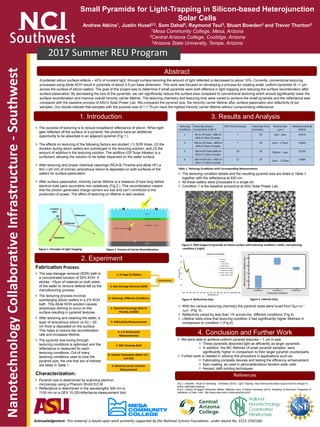
2017 NCI-SW Summer REU Poster
- 1. 2017 Summer REU Program NanotechnologyCollaborativeInfrastructure-Southwest Acknowledgement: This material is based upon work primarily supported by the National Science Foundation under award No. ECCS-1542160. Small Pyramids for Light-Trapping in Silicon-based Heterojunction Solar Cells Andrew Atkins1, Justin Huxel2,3, Som Dahal3, Raymond Tsui3, Stuart Bowden3 and Trevor Thorton3 1Mesa Community College, Mesa, Arizona 2Central Arizona College, Coolidge, Arizona 3Arizona State University, Tempe, Arizona Abstract 1. Introduction 2. Experiment 3. Results and Analysis 4. Conclusion and Further Work References A polished silicon surface reflects ~ 40% of incident light; through surface texturing the amount of light reflected is decreased to about 10%. Currently, conventional texturing processes using dilute KOH result in pyramids of about 3-5 μm base dimension. This work was focused on developing a process for creating small, uniform pyramids of ~1 µm across the surface of silicon wafers. The goal of this project was to determine if small pyramids were both effective in light trapping and reducing the surface recombination after surface passivation. By decreasing the size of the pyramids, we can significantly reduce the surface area compared to conventional texturing which should significantly lower the surface recombination and improve overall minority carrier lifetime. The texturing chemistry and texturing time were varied to achieve the small pyramids and the reflectance was compared with the baseline process of ASU’s Solar Power Lab. We compared the pyramid size, the minority carrier lifetime after surface passivation and reflectivity of our samples. Our results indicate that samples with the pyramid size of 1-1.75 µm have the highest minority carrier lifetime without compromising reflectance. ❖ The purpose of texturing is to reduce broadband reflectance of silicon. When light gets reflected off the surface of a pyramid, the photons have an additional opportunity to be absorbed in an adjacent pyramid (Fig 1.). ❖ The effects on texturing of the following factors are studied: (1) SDR times, (2) the duration during which wafers are submerged in the texturing solution, and (3) the amount of additive in the texturing solution. The additive (GP Solar Alkatex) is a surfactant, allowing the solution to be better dispersed on the wafer surface. ❖ After texturing and proper chemical cleanings (RCA-B, Piranha and dilute HF) a thin (~20 nm) of intrinsic amorphous silicon is deposited on both surfaces of the wafers for surface passivation. ❖ After surface passivation, minority carrier lifetime is a measure of how long before electron-hole pairs recombine non-radiatively (Fig 2.). This recombination means that the photon generated charge carriers are lost and can’t contribute to the production of power. The effect of texturing on lifetime is also studied. Characterization: Fabrication Process: ❖ The saw damage removal (SDR) bath is a concentrated solution of 30% KOH. It etches ~15µm of material on both sides of the wafer to remove defects left by the manufacturing process. ❖ The texturing process involves submerging silicon wafers in a 2% KOH bath. This dilute KOH solution causes anisotropic etching to occur on the surface resulting in pyramid textures. ❖ After texturing and cleaning the wafer, a layer of amorphous silicon (a-Si) ~ 20 nm thick is deposited on the surface. This helps to reduce the recombination rate and increases lifetime. ❖ The pyramid size tuning through texturing conditions is optimized and the reflectance is measured for each texturing conditions. Out of many texturing conditions used to tune the pyramid size, the one that are of interest are listed in Table 1. ❖ Pyramid size is determined by scanning electron microscopy using a Phenom World S.E.M ❖ Reflectance is determined in the wavelengths 300 nm to 1100 nm on a QEX 10 QE/reflectance measurement tool. Figure 1. Principle of Light Trapping Figure 2. Process of Carrier Recombination ❖ We were able to achieve uniform pyramid textures ~ 1 um in size. ❖ These pyramids absorbed light as efficiently as larger pyramids. ❖ In addition, the MC lifetimes of small pyramid samples were significantly higher in comparison to their larger pyramid counterparts. ❖ Further work is needed in utilizing this procedure in applications such as: ❖ Fabricating complete devices and testing the efficiency enhancement ❖ Spin-coating, as used in perovskite/silicon tandem solar cells. ❖ Aerosol Jet® printing techniques. 2. Saw Damage Removal (SDR) 3. Texturing: Different Conditions 4. Chemical Cleanings (RCA-B, Piranha, & BOE) 5. Reflectivity Measurements 6. S.E.M (Pyramid Measurements) 7. BOE Cleaning Bath 1. N-Type CZ Wafers 8. Surface Passivation (20nm of i- a:Si (H)) 9. Minority Carrier Lifetime Measurement Bulk Resistance Texturing Conditions Texturing solution composition at 80 oC SDR Time (minutes) Texturing Time (minutes) Pyramid Size ( µm ) Reflectance(%) @ 630nm 1 50 mL GP Solar + 800 ml KOH+17 liters DI water 7 25 2µm - 5µm 8.01% 2 200 mL GP Solar + 800 ml KOH+17 liters DI water 7 10 1µm – 1.75µm 8.36% 3 200 ml GP Solar+800 ml KOH+17 Liters DI water 10 10 700nm – 1µm 8.15% 4 200 ml GP solar + 800 ml KOH+ 17 liters DI water 12 10 1µm – 1.25µm 8.08% Table 1. Texturing Conditions with Corresponding Measurements Figure 3. SEM Images of pyramids on silicon surface with texturing condition 1 (left), and texturing condition 2 (right) Figure 4. Reflectivity Data Figure 5. Lifetime Data ❖ With the various texturing chemistry the pyramid sizes were tuned from 5µm to ~ 1µm (Fig. 3). ❖ Reflectivity varied by less than 1% across the different conditions (Fig 4). ❖ Lifetime tests show that texturing condition 2 had significantly higher lifetimes in comparison to condition 1 (Fig 5). ❖ The texturing condition details and the resulting pyramid size are listed in Table 1. together with the reflectance at 630 nm. ❖ All these wafers were processed in a single lot. ❖ Condition 1 is the baseline procedure at ASU Solar Power Lab. 2.08 µm 2.68 µm 5.31 µm 2.26 µm 1.56 µm 1.15 µm 1.34 µm 1.72 µm (Fig 1.) Bowden, Stuart & Honsberg, Christiana (2010). Light Trapping. http://www.pveducation.org/pvcdrom/5-design-of- silicon-cells/light-trapping (Fig 2.) Glitzky, Annegret, Alexander Mielke, Matthias Liero, & Reiner Nürnberg (2014). Modeling of Electronic Properties of Interfaces in Solar Cells. http://www.wias-berlin.de/people/liero/d22/