Recommended

Recommended
More Related Content
What's hot
What's hot (20)
Similar to BAPVC Poster Fall 2016
Similar to BAPVC Poster Fall 2016 (20)
Recently uploaded
Recently uploaded (20)
BAPVC Poster Fall 2016
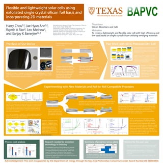
- 1. Flexible and lightweight solar cells using exfoliated single crystal silicon foil basis and incorporating 2D materials Harry Chou1,3, Jae Hyun Ahn1,2, Rajesh A Rao4, Leo Mathew4, and Sanjay K Banerjee1,2,3 Thrust Area Silicon Absorbers and Cells Motivation To create a lightweight and flexible solar cell with high efficiency and low cost based on single crystal silicon utilizing emerging materials 1Microelectronics Research Center, The University of Texas at Austin, Austin, Texas 78758, USA 2Department of Electrical and Computer Engineering, The University of Texas at Austin, Austin, Texas 78758, USA 3Materials Science and Engineering Program, University of Texas at Austin, Austin, Texas 78712, USA 4Applied Novel Devices Inc., Austin, Texas 78717, USA The Basis of Our Device Past Work with All-IC Processes DHJ Cell Experimenting with New Materials and Roll-to-Roll Compatible Processes We demonstrated a dual heterojunction (DHJ) cell fabricated by additional thin film and surface processes to form junctions and contacts. The α-Si dual heterojunction cell had a peak 19.4% efficiency (14.9% PCE on Si foil). Onyegam, E. U., Sarkar, D., Hilali, M. M., Saha, S., Mathew, L., Rao, R. A., … Banerjee, S. K. (2014). Realization of dual-heterojunction solar cells on ultra-thin ∼ 25 μ m, flexible silicon substrates. Applied Physics Letters, 104(15), 0–4. http://doi.org/10.1063/1.4871503 Hilali, M. M., Saha, S., Onyegam, E., Rao, R., Mathew, L., & Banerjee, S. K. (2014). Light trapping in ultrathin 25 μm exfoliated Si solar cells. Applied Optics, 53(27), 6140–7. http://doi.org/10.1364/AO.53.006140 Process begins with a single crystal Si wafer. Seed layer of Ti is deposited on one side of the wafer for electroplating. Thick film of Ni is plated onto the thin Ti film. The structure is heated and the coefficient of thermal expansion (CTE) difference between the Ni and the Si induces stress. Cracking initiates and spreads laterally to relieve the stress and the foil is exfoliated off of the wafer surface. The parent wafer can return to the beginning of the process to be exfoliated again. Multiple foils can be made from a single wafer. Onyegam, E. U. (2014). Remote Plasma Chemical Vapor Deposition for High Efficiency Heterojunction Solar Cells on Low Cost , Ultra-Thin , Semiconductor- on-Metal Substrates. The University of Texas at Austin. To reduce the number of vacuum and high temperature process steps that the Si foil experiences (thereby lowering cost) we experiment with other materials, 2 dimensional materials. Graphene is a mechanically flexible, optically transparent, and high mobility semimetal. We can grow single layer graphene (SLG) or multi layer graphene (MLG) by CVD. Others have demonstrated that graphene growth and transfer are roll-to-roll compatible. Li, X., Cai, W., Colombo, L., & Ruoff, R. S. (2009). Evolution of graphene growth on Ni and Cu by carbon isotope labeling. Nano Letters, 9(12), 4268–72. http://doi.org/10.1021/nl902515k Kobayashi, T., Bando, M., Kimura, N., Shimizu, K., Kadono, K., Umezu, N., … Hobara, D. (2013). Production of a 100-m-long high- quality graphene transparent conductive film by roll-to-roll chemical vapor deposition and transfer process. Applied Physics Letters, 102(2), 1–5. http://doi.org/10.1063/1.4776707 Work by Sony Advanced Materials Laboratories Process cost analysis Research needed to transition technology to industry Summary of progress versus plans Metrics for the next year On one path of study, we incorporate multiple layers of 2D materials. Here, insulating h-BN. On another path, we deposit a thin film Al2O3, with superior passivation and dielectric properties. Graphene acts as both the transparent conducting electrode in the device as well as forming the junction. It is doped p-type with AuCl3 coating as a charge transfer dopant. Acknowledgement: This work is supported by the Department of Energy through the Bay Area Photovoltaic Consortium under Award Number DE-EE0004946 Directly forming a junction between graphene and Si gives high recombination. By inserting an insulating electron blocking layer between graphene and Si, recombination is suppressed. This film can also serve to passivate the Si surface and improve VOC. Doping the graphene layer increases the carrier concentration and further improves device performance. At left, the amount of doping (spin coating AuCl3 in Nitromethane) correlates positively with device performance. The dopant reduces the resistance of the graphene layer, thereby enhancing the device ability to separate charge. To further boost the graphene current-carrying ability we introduced multi-layer graphene which further improved performance. We also compare the oxide insulating layer GIS cell with the h-BN insulating layer GIS cell. • Fabricate a graphene and exfoliated single crystal silicon foil single junction device with > 15% PCE • Improve growth and transfer of still more 2D materials for use as the I-layer in the GIS cell (or GSS cell) • 2D materials such as h-BN, MoS2, MoSe2, etc. Considerable resources will be needed to improve process integration (roll-to-roll, etc.) but these are considered engineering development, rather than research. Research is needed to find trap and recombination sites at surfaces and interfaces, to characterize dopant distribution and uniformity, and to improve material quality. The above milestones in blue have been reached. We have DHJ cell with peak 19.4% PCE (14.9% PCE on Si foil) and GIS cell with peak 7.8% PCE (4.8% on Si foil)