SlideShare a Scribd company logo
1 of 199
Download to read offline
Linear Integrated Circuits
Integrated Circuit (IC)
If multiple electronic components are interconnected on a single chip of
semiconductor material, then that chip is called as an Integrated Circuit (IC). It
consists of both active and passive components.
Computers, mobile phones and other digital home appliances are now inextricable
parts of the structure of modern societies, made possible by the low cost of
integrated circuits.
In 1958 Jack Kilby of Texas Instruments invented first IC
Introduction
Advantages of Integrated Circuits
Integrated circuits offer many advantages.
1. Compact size: For a given functionality, you can obtain a circuit of smaller size
using ICs, compared to that built using a discrete circuit.
2. Lesser weight: A circuit built with ICs weighs lesser when compared to the
weight of a discrete circuit that is used for implementing the same function of IC.
3. Low power consumption: ICs consume lower power than a traditional circuit,
because of their smaller size and construction.
4. Reduced cost: ICs are available at much reduced cost than discrete circuits
because of their fabrication technologies and usage of lesser material than
discrete circuits.
5. Increased reliability: Since they employ lesser connections, ICs offer increased
reliability compared to digital circuits.
6. Improved operating speeds: ICs operate at improved speeds because of their
switching speeds and lesser power consumption.
Introduction
Types of Integrated Circuits Integrated circuits are of two types:
•Analog Integrated Circuits
•Digital Integrated Circuits
Analog Integrated Circuits
Integrated circuits that operate over an entire range of continuous values of the signal
amplitude are called as Analog Integrated Circuits.
Linear Integrated Circuits: An analog IC is said to be Linear, if there exists a linear
relation between its voltage and current.
IC 741, an 8-pin Dual In-line Package (DIP)op-amp, is an example of Linear IC.
Digital Integrated Circuits
If the integrated circuits operate only at a few pre-defined levels instead of operating
for an entire range of continuous values of the signal amplitude, then those are called
as Digital Integrated Circuits.
Introduction
Pn junction
isolation
Hybrid circuits
Integrated circuits
Dielectric
isolation
Monolithic circuits
Bipolar Uni polar
MOSFET JFET
Classification of ICs
Thick
&Thin film
Introduction
Types of ICs Based on the method or techniques used in manufacturing them, types
of ICs can be divided into three classes:
1. Thin and thick film ICs:
• In thin or thick film ICs, passive components such as resistors, capacitors are
integrated but the diodes and transistors are connected as separate components
to form a single and a complete circuit.
• Thin and thick ICs that are produced commercially are merely the combination
of integrated and discrete (separate) components.
2. Monolithic ICs:
• In monolithic ICs, the discrete components, the active and the passive and also
the interconnections between then are formed on a silicon chip.
• The word monolithic is actually derived from two Greek words “mono”
meaning one or single and Lithos meaning stone. Thus monolithic circuit is a
circuit that is built into a single crystal.
Introduction
Types of ICs Based on the method or techniques used in manufacturing them, types
of ICs can be divided into three classes:
3. Hybrid or Multi chip ICs:
• As the name implies, “Multi”, more than one individual chips are
interconnected.
• The active components that are contained in this kind of ICs are diffused
transistors or diodes. The passive components are the diffused resistors or
capacitors on a single chip
Introduction
Chip size and Complexity
• Invention of Transistor (Ge) - 1947
• Development of Silicon - 1955-1959
• Silicon Planar Technology - 1959
• First ICs, SSI (3- 30gates/chip) - 1960
• MSI ( 30-300 gates/chip) - 1965-1970
• LSI ( 300-3000 gates/chip) -1970-1975
• VLSI (More than 3k gates/chip) - 1975
• ULSI (more than one million active devices are integrated on single chip)
Introduction
Introduction
IC Package types:
• Metal can Package
• Dual-in-line
• Flat Pack
Metal can Packages
• The metal sealing plane is at the bottom over which the chip is bounded
• It is also called transistor pack
Introduction
IC Package types:
• Metal can Package
• Dual-in-line
• Flat Pack
Doul-in-line Package
• The chip is mounted inside a plastic or ceramic case
• The 8 pin Dip is called MiniDIP and also available with 12, 14, 16, 20pins
Introduction
IC Package types:
• Metal can Package
• Dual-in-line
• Flat Pack
Flat Pack
The chip is enclosed in a rectangular ceramic case
Introduction
Selection of IC Package
Type Criteria
Metal can
package
1. Heat dissipation is important
2. For high power applications like power amplifiers,
voltage regulators etc.
DIP 1. For experimental or bread boarding purposes as easy
to mount
2. If bending or soldering of the leads is not required
3. Suitable for printed circuit boards as lead spacing is
more
Flat pack 1. More reliability is required
2. Light in weight
3. Suited for airborne applications
Introduction
Fairchild - µA, µAF
National Semiconductor - LM,LH,LF,TBA
Motorola - MC,MFC
RCA - CA,CD
Texas Instruments - SN
Signetics - N/S,NE/SE
Burr- Brown - BB
Manufacturer’s Designation for Linear ICs
Introduction
1. Military temperature range : -55o C to +125o C (-55o C to +85o C)
2. Industrial temperature range : -20o C to +85o C (-40o C to +85o C )
3. Commercial temperature range : 0o C to +70o C (0o C to +75o C )
Temperature Ranges
Introduction
Pin Identification
Analog Signal Processing
Signal
Anything that carries some information is called a signal.
A signal is also defined as a physical quantity that varies with time, space or any
other independent variable.
A signal may be represented in time domain or frequency domain.
Human speech is a familiar example of a signal. Electric current and voltage are also
examples of signals.
System
A system is defined as an entity that acts on an input signal and transforms it into an
output signal.
A system is also defined as a set of elements or fundamental blocks which are
connected together and produces an output in response to an input signal.
Signal Processing
Signal processing is a method of extracting information from the signal which in turn
depends on the type of signal and the nature of information it carries.
Analog Signal Processing
Analog signal processing (ASP) is a signal processing conducted on analog signals
by analog means.
Analog indicates something that is mathematically represented as a set of continuous
values.
This differs from digital which uses a series of discrete quantities to represent signal.
Analog values are typically represented as a voltage, electric current or electric
charge around components in the electronic devices.
An error or noise affecting such physical quantities will result in a corresponding
error in the signals represented by such physical quantities.
Examples of analog signal processing include all sorts of analog active filters, such
as crossover filters in loudspeakers, bass, treble and volume controls on stereos, and
tint controls on TV‟s.
Common analog processing elements include operational amplifiers (Op-Amps), and
operational trans-conductance amplifiers (OTA‟s) in addition to passive
components.
Analog Signal Processing
Continuous-Time Signals & Systems
A system is considered continuous if the signal exists for all time.
Frequently, the terms "analog" and "continuous" are usually employed
interchangeably, although they are not strictly the same.
Assume a continuous-time system with impulse response h(t), as shown in the
following figure.
The system processes the continuous-time input signal x(t) in some way, and
produces an output y(t).
At any value of time, t, we input a value of x(t) into the system and the system
produces an output value for y(t).
For instance, if we have a multiplier system whose input/output relation is given by
y(t) = 7x(t), and the input value x(t) = sin(wt) then the output is y(t) = 7sin(wt).
Analog Signal Processing
Analog and Digital Signals
Digital Signal Processing
To perform digitally, there is need for an interface between analog signal and digital
processor at input side. This interface is known as an analog to digital (A/D)
converter.
Similarly, an interface between digital signal and analog processor at output side.
This interface is known as an digital to analog (D/A) converter.
WHY Analog Signal Processing ?
The main disadvantages of DSP are
1. Additional complexity (A/D & D/A Converters)
2. Limit in frequency. High speed AD converters are difficult to achieve in practice.
In high frequency applications DSP are not preferred.
3. High cost analog-digital conversion, high power consumption
To overcome these drawbacks we prefer analog signal processing
Analog signals are processed directly by appropriate analog systems (such as filters
or frequency analyzers) or frequency multipliers for the purpose of changing their
characteristics or extracting some information.
Introduction to Operational Amplifier
Operational amplifier:
Operational amplifier is popularly known as op amp. From its initial application in
analog computers to perform mathematical operations such as addition, subtraction,
integration, and differentiation, it had the popular name ‘operational amplifier’.
1. Operational amplifiers are used in many industrial, commercial, and consumer
electronic gadgets.
2. It is a high gain voltage amplifier.
3. It has many applications such as differential amplifier, voltage comparator,
instrumentation amplifier, isolation amplifier (voltage follower for impedance
matching application among different stages of amplifiers), and Schmitt trigger
applications in waveform generators.
4. Op amp in open-loop configuration functions as a voltage comparator with very
large values of gain. Voltage comparator circuits find many applications in
Schmitt trigger, etc.
5. Due to the addition of negative feedback to operational amplifier (closed-loop
configuration), it has finite values of gain.
6. Operational amplifiers using positive feedback circuit function as oscillator
circuits.
Introduction to Operational Amplifier
The IC is considered as a “black box” device and referred to its schematic structure
as in Figure.
The general purpose op-amp is of the differential type with both inverting and non-
inverting inputs.
Block Diagram of an Operational Amplifier
An operational amplifier is a multistage amplifier consisting four internal blocks
Basic building blocks inside an op amp IC are as follows:
1. First-stage differential amplifier.
2. Second-stage differential amplifier.
3. Voltage-level shifter.
4. Power output stage.
Block Diagram of an Operational Amplifier
First-Stage differential amplifier
It consists of a dual input, balanced output differential amplifier.
Its function is to amplify the difference between the two input signals.
It provides high differential gain, high input impedance and low output impedance.
First stage has two input terminals. It has the facility to operate on two signals
working in differential mode of operation.
(a) One input is known as ‘inverting (INV) input signal’.
(b) Second input is known as ‘non-inverting (NINV) input signal’.
Contributes to higher values of common-mode rejection ratio (CMRR).
Second-Stage differential amplifier
The overall gain requirement of an Op-Amp is very high. Since the input stage alone
cannot provide such a high gain.
Second stage is used to provide the required additional voltage gain.
It consists of another differential amplifier with dual input, and unbalanced (single
ended) output.
Block Diagram of an Operational Amplifier
Voltage level shifting stage
As the Op-Amp amplifies even D.C signals, the small D.C. quiescent voltage level
of previous stages may get amplified and get applied as the input to the next stage
causing distortion the final output.
Hence the level shifting stage is used to bring down the D.C. level to ground
potential, when no signal is applied at the input terminals.
Output stage
It consists of a push-pull complementary amplifier which provides large A.C. output
voltage swing and high current sourcing and sinking along with low output
impedance.
BJT Differential Amplifier
Differential Amplifier
• Amplifies the difference between two voltages applied at its inputs and produces an
output voltage.
• Rejects the common mode or average of the two input signal voltages.
• BJT differential amplifier is one of the building blocks of operational amplifier ICs.
• The differential amplifier is also known as difference amplifier.
• The differential pair is also known as emitter-coupled pair.
Condition for DF
Matched transistor are used (properties are same )
Βeta is large (Ic =Ie)
BJT Differential Amplifier
Working Principles of Differential Amplifier
Two identical transistors T1 and T2 are connected in common-emitter transistor operation
with symmetrical configuration.
Differential amplifier has the provision to connect two input voltages Vin (1) and Vin (2) and
obtain two output voltages Vout (1) and Vout (2).
The difference between the two output voltages is taken as a single output voltage Vout from
the amplifier.
BJT Differential Amplifier
The circuit is designed for equal biasing voltages VBE1 and VBE2, so that the biasing
voltage becomes VBE = 0.7 V for the two identical transistors.
Emitter terminals of the two transistors are connected together.
The resulting DC bias current IE through RE will be shared equally by the two
transistors T1 and T2.
Each transistor shares 0.5 IE to contribute to total emitter current IE through the
emitter resistor RE
The two collector currents IC
(1) and IC (2) are equal to 0.5
IC. Each transistor collector
current IC = 0.5 IE.
Total current IE is the sum of
the two DC collector currents
of each transistor.
The output voltages Vout (1)
and Vout (2) are developed at
the two collector points, when
the input signal voltages are
applied.
BJT Differential Amplifier
The output can be taken from any one of the output terminals and ground. Then, the
amplifier operation is single-ended output differential amplifier.
The difference of the two output voltages Vout (1) and Vout (2) functions as a single
output voltage Vout. Then, it is known as double-ended output arrangement.
For a perfectly symmetrical amplifier, the output voltage
Vout = AD [Vin (1) - Vin (2)],
BJT Differential Amplifier
Main Features of the Differential Amplifier
Very large gain occurs when opposite signals are applied to both the input terminals.
Difference voltage between the two inputs:
Vd = [Vin (1) - Vin (2)]
The difference signal Vd is amplified with gain AD. Amplified output voltage (for
differential inputs)
Vout (D) = AD [Vin (1) - Vin (2)]
Very small gain occurs when common type signals are applied to the two input
terminals (for common inputs)
The overall operation is to amplify the differential signals, while rejecting the
common signals at the two inputs. However, total output voltage
Vout = Vout (D) + Vout(C)
Main Features of the Differential Amplifier
Common signals in the amplifier undergo attenuation (due to cancellation) of the
noise (unwanted) input signals. This feature is known as common-mode rejection
(CMMR).
Since the amplification of the opposite signals is much greater than that of the
common-mode input signals, the amplifier provides a CMMR.
CMRR = AD/AC
CMRR(dB) = 20 log10 (AD/AC)
Usually, differential amplifiers with larger values of CMRR are used.
It measures how well the differential amplifier attenuates or rejects the common-
mode signals.
The amplifier is virtually free from interfering signals.
The signal to noise ratio will be improved by a factor of the value of CMRR.
Example
Calculate the dc voltages and currents in the circuit of Fig.
Example
Calculate the dc voltages and currents in the circuit of Fig.
JFET Differential Amplifier
This is equal to the gain of common source FET amplifier
JFET Differential Amplifier
Example
In the JFET differential amplifier, gm = 1.41milimhos. Calculate the following:
1. DC output voltage.
2. Gain of single-ended amplifier.
3. Gain of double-ended amplifier.
Example
Example
Single-ended Differential Amplifier
When one input signal Vin is applied to one of the input terminals of the two
transistors, while the second input terminal of the other transistor is grounded, the
electronic amplifier is known as single-ended amplifier.
Single-ended Differential Amplifier
Transistor T1 acts as common-emitter transistor amplifier. Therefore, amplified
output voltage Vout (1) of transistor T1 is 180° out-of-phase with input signal
voltage.
Transistor T2 functions as common base transistor amplifier. Amplified output
voltage Vout (2) will be in-phase with input signal Vin.
Double-ended Differential Amplifier
When two equal input signals Vin (1) and Vin (2) of opposite polarity are applied to
the two inputs of differential amplifier, and two outputs are available, the electronic
amplifier is known as double-ended differential amplifier
The difference between the two equal and opposite polarity input signals is double
the magnitude of each signal. Therefore, the amplifier provides large gain.
Common-Mode Differential Amplifier
When the same input signal is applied to both the input terminals of the two
transistors of the differential amplifier, the electronic amplifier is considered to be in
common-mode operation of the amplifier.
Therefore, the input signals to the two transistors are in-phase and equal in
magnitude.
The common-mode input signals get
cancelled or not amplified by the
differential amplifier because it is
designed to amplify only the
differential signals
Why Voltage-level Shifter is used?
Voltage-level Shifter (Intermediate Stage Between the Input and the Output Stages)
The first two stages of differential amplifiers are DC amplifiers.
Therefore, the DC voltage level at the output collector terminal of the second stage
will be high.
This DC voltage gets propagated to output port along with the AC voltage in normal
amplifier chain. It is undesirable.
Using DC voltage-level shifter circuit, necessary correction is made to feed it to the
input stage of last stage
Voltage-level Shifter
We begin the analysis by using KVL in the input loop of Figure and letting vin = 0 to
obtain
Above Equation shows that by varying RE, Vout can be set to any
desired dc level (limited to a maximum of VBB–VBE).
Since VBB is the dc level acquired from the previous stage, this
amplifier is used to shift the level downward (to a lower value).
If upward shifting is required, a similar circuit is used
but pnp transistors are substituted for the npn transistors.
Output Stage of Operational Amplifier
1. It is push–pull complementary symmetry amplifier/Darlington pair amplifier.
2. It has low output impedance Zout.
3. It has large output swing and current carrying capability.
Output Stage of Operational Amplifier
Darlington pair amplifier.
Characteristics of Ideal Op-amp
The op-amp is said to be ideal if it has the following characteristics.
1. Infinite voltage gain A.
2. Infinite input resistance Ri.
3. Zero output resistance Ro.
4. Zero output offset.
5. Infinite bandwidth.
6. Infinite common mode rejection ratio.
7. Infinite slew rate.
Equivalent circuit of op-amp
An Op-Amp can be realized by Thevenin‟s equivalent circuit.
Where voltage controlled source AOLVd is an equivalent Thevenin voltage source and
R0 is the Thevenin resistance.
Various Types of operational amplifiers
The very first series of modular solid-state op-amps were introduced by Burr-Brown
Research Corporation and G.A. Philbrick Researches Inc. in 1962
Internal Blocks of Operational Amplifier IC
μA 741 Op-Amp
Operational amplifier is an IC.
The schematic circuit symbol of op amp is shown in Fig.
Op amp (μA 741) is mostly used in the industrial applications and the laboratories
in the colleges.
Op amp IC has two input terminals, one output terminal, and two supply voltage
connection terminals for making circuit connections for applications.
There will be some other pins depending upon the IC package.
The magnitude of supply voltages and the pin number details of IC are provided in
the manufacturer’s data manuals of selected op amp.
Pin Configuration of μA 741 Op-Amp
Dual-in-line plastic package and metal can package are shown in Figure
The DC amplifiers have very large gain operating with two input signal voltages V1
and V2 producing one output voltage Vout. Supply voltages are ± 5 V and ± 15 V.
Pin Configuration of μA 741 Op-Amp
Pin-1: Offset null terminal.
Pin-2: Inverting (INV) input terminal. All input signals connected to this terminal
on op amp will appear at the output terminal with 180° phase shift.
Pin-3: Non-inverting (N-INV) input terminal. All input signals applied to this
terminal on op amp appears as it is in waveform (shape) at the output terminal.
Changes occur only in levels of amplitudes at the output voltage.
Pin-4: Supply voltage - VCC (negative supply voltage terminal).
Pin-5: Offset null terminal.
Pin-6: Output terminal; output signal.
1. Output signal will have 180° phase shift to input signals applied to inverting input
terminal pin-2.
2. Output signal will be in-phase to input signals applied to non-inverting input
terminal
pin-3.
3. Output signal depends upon the voltage gain of operational amplifier.
Pin-7: supply voltage +VCC terminal (positive supply voltage terminal).
Pin-8: no connection.
Different types of op amps
(a) μA 741 simple and popular type operational amplifier,
(b) LT 1056 op amp gas JFET device at its input stage,
(c) low power CMOS op amp IC is LMC 660,
(d) medium power op amp IC is LM 675,
(e) high power operational
amplifier IC is LM 12, and
(f) LT1220 and LT 1221 are high frequency op amps.
Schematic Diagram Of Op-Amp
1. Outside connection from pin-3 is non-inverting (N-NIV) input terminal. V1 is the
input voltage at pin-3.
2. +sign at N-NIV terminal indicates that input voltage applied at pin-3 appears at
output terminal (6) with zero phase shift.
3. Terminal pin-2 is the inverting (INV) input terminal. V2 is the input voltage at pin-
2. − Sign at INV terminal indicates that the input voltage applied at pin-2 appears at
the output terminal (6) with 180° phase shift.
4. Terminal 6 is output terminal (Vout is the output voltage at pin-6).
Schematic Diagram Of Op-Amp
Differential input voltage:
Input voltages V1 and V2 are known as single-ended voltages. All voltages in the
operational amplifier are referred with respect to common terminal AC ground.
Differential mode voltage VD is the difference between the two input voltages V1 and
V2 Therefore, differential input voltage VD = (V1 - V2).
Output voltage: Vout = [A (V1 - V2)] = (AVd), where A = amplifier gain.
Common-mode voltage:
Common-mode input voltage VC is the average value of two input voltages V1 and V2.
A very small gain occurs for common inputs.
Total (overall) voltage of the operational amplifier due to the presence of differential
mode and common-mode input voltages.
Characteristic of an Ideal Op-Amp
Infinite open-loop gain:
If there is no feedback connection between the output and the input terminals of
operational amplifier, it is considered to be in open-loop condition. The operational
amplifier will have infinite open-loop gain
If the gain A is
infinite, how are
we going to use the
op amp?
In almost all
applications the op amp
will not be used alone in
a so-called open-loop
configuration. Rather,
we will use other
components to apply
feedback to close the
loop around the op
amp,
For 741C it is typically 200,000
Characteristic of an Ideal Op-Amp
Infinite input resistance Ri:
Ideal op-amp offers infinite input resistance and hence the ideal op-amp draws no
current (i1=i2=0).
For 741C it is of the order of 2MΩ
Characteristic of an Ideal Op-Amp
Zero output resistance Ro:
Ideal op-amp offers zero output resistance so that the output can drive an infinite
number of other devices.
For op-amp 741 it is 75Ω
Characteristic of an Ideal Op-Amp
Why high i/p
impedance and low
o/p impedance
We want that the amplified
signal does not go any
further voltage drop and
captures its maximum
across Rl
Characteristic of an Ideal Op-Amp
Zero output offset:
The output offset is the output voltage of an amplifier when both inputs are grounded
output voltage, when input voltage is zero. Ideal op-amp possesses zero output offset.
Infinite bandwidth:
An ideal operational amplifier has an infinite frequency response and can amplify any
frequency signal from DC to the highest AC frequencies without attenuation.
Infinite common mode rejection ratio:
Common-mode rejection ratio (CMRR) is defined as the ratio of the differential
voltage amplification to the common-mode voltage amplification.
For op-amp 741C CMRR is 90 dB
Characteristic of an Ideal Op-Amp
Infinite slew rate:
Slew rate, SR, is the rate of change in the output voltage caused by a step input.
Its units are V/μs or V/ms.
Higher the slew rate, faster is the op-amp.
Ideal Op-Amp has Infinite slew rates so that output voltage changes occur
simultaneously with input voltage changes.
Ideal Op-Amp Equivalent Circuit
The Inverting Configuration
There are two basic circuit configurations employing an op amp and two resistors:
1. The inverting configuration and
2. The non-inverting configuration
Inverting configuration
Figure shows the inverting configuration.
It consists of one op amp and two resistors R1 and R2.
Negative feedback Resistor R2 is connected from the output terminal of the op
amp, terminal 3, back to the inverting or negative input terminal
If R2 were connected between terminals 3 and 2 we would have called this
positive feedback.
The Inverting Configuration
Closed Loop Gain
Closed-loop gain G, is defined as
The gain A is very large (ideally infinite).
The voltage between the op-amp input terminals should be negligibly small and
ideally zero.
It follows that the voltage at the inverting input terminal (v1) is given by v1 = v2.
The Inverting Configuration
Virtual Ground Concept
V1= V2
A virtual short circuit means that whatever voltage is at 2 will automatically appear
at 1 because of the infinite gain A.
Terminal 2 is connected to ground; thus v2 = 0 and v1 = 0.
Now we can say that terminal 1 is being a virtual ground—that is, having zero
voltage but not physically connected to ground.
We say that two input terminals
“tracking each other in potential”
OR
“virtual short circuit” that exists
between the two input terminals
The Inverting Configuration
Analysis
The minus sign means that the closed-loop amplifier provides signal inversion.
The Inverting Configuration
The fact that the closed-loop gain depends entirely on external passive components
(resistors R1 and R2) is very significant.
It means that we can make the closed-loop gain as accurate as we want by selecting
passive components of appropriate accuracy.
It also means that the closed-loop gain is (ideally) independent of the op-amp gain.
We started out with an amplifier having very large gain A, and through applying
negative feedback we have obtained a closed-loop gain R2/R1 that is much smaller
than A but is stable and predictable.
That is, we are trading gain for accuracy.
The Inverting Configuration
Effect of Open loop gain:
If we denote the output voltage VO, then the voltage between the two input
terminals of the op amp will be VO/A. Since the positive input terminal is grounded,
the voltage at the negative input terminal must be − VO/A
The output voltage VO
The Inverting Configuration
To minimize the dependence of the closed-loop gain G on the value of the open-
loop gain A, we should make
Input and Output Resistances:
to avoid the loss of signal
strength, voltage amplifiers
are required to have high
input resistance
The Inverting Configuration
Input and Output Resistances:
In the case of the inverting op-amp configuration we are studying, to make Ri high
we should select a high value for R1.
However, if the required gain R2/R1 is also high, then R2 could become
impractically large (e.g., greater than a few megohms).
We may conclude that the inverting configuration suffers from a low input
resistance
Example
Assuming the op amp to be ideal, derive an expression for the closed-loop gain
VO/VI of the circuit shown in Fig. Use this circuit to design an inverting amplifier
with a gain of 100 and an input resistance of 1M. Assume that for practical reasons
it is required not to use resistors greater than 1 M.
Example
Assuming the op amp to be ideal, derive an expression for the closed-loop gain
VO/VI of the circuit shown in Fig. Use this circuit to design an inverting amplifier
with a gain of 100 and an input resistance of 1MΩ. Assume that for practical
reasons it is required not to use resistors greater than 1 M Ω.
Example
Example
Now, since an input resistance of 1 M Ω is required, we select R1 = 1M Ω.
Then, with the limitation of using resistors no greater than 1M Ω, the maximum
value possible for the first factor in the gain expression is 1 and is obtained by
selecting R2 =1M Ω.
To obtain a gain of −100, R3 and R4 must be selected so that the second factor in
the gain expression is 100. If we select the maximum allowed (in this example)
value of 1 M for R4, then the required value of R3 can be calculated to be 10.2 k
Ω.
The Weighted Summer
A very important application of the inverting configuration is the weighted-summer
circuit shown in Fig.
Here we have a resistance Rf in the negative-feedback path (as before), but we have
a number of input signals v1,v2, . . . ,vn each applied to a corresponding resistor
R1,R2, . . . ,Rn, which are connected to the inverting terminal of the op amp.
The Weighted Summer
The output voltage Vo
That is, the output voltage is a weighted
sum of the input signals v1,v2, . . . ,vn.
This circuit is therefore called a weighted
summer. Note that each summing
coefficient may be independently adjusted
by adjusting the corresponding “feed-in”
resistor (R1 to Rn).
The Weighted Summer
Weighted summers are utilized in a variety of applications including in the design of
audio systems, where they can be used in mixing signals originating from different
musical instruments.
The Non-Inverting Configuration
In this configuration the input signal VI is applied directly to the positive input
terminal of the op amp while one terminal of R1 is connected to ground.
The Closed-Loop Gain
Assuming that the op amp is ideal with infinite gain, a virtual short circuit exists
between its two input terminals. Hence the difference input signal is
The Non-Inverting Configuration
The current into the op-amp inverting input is zero, the circuit composed of R1 and R2
acts in effect as a voltage divider feeding a fraction of the output voltage back to the
inverting input terminal of the op amp; that is,
Then the infinite op-amp gain and the resulting virtual short circuit between the two
input terminals of the op amp forces this voltage to be equal to that applied at the
positive input terminal; thus,
The Non-Inverting Configuration
Degenerative feedback
Let VI increase. Such a change in VI will cause VID to increase, and VO will
correspondingly increase as a result of the high (ideally infinite) gain of the op amp.
However, a fraction of the increase in VO will be fed back to the inverting input
terminal of the op amp through the (R1,R2) voltage divider.
The result of this feedback will be to counteract the increase in VID, driving VID back
to zero, albeit at a higher value of VO that corresponds to the increased value of VI.
This degenerative action of negative feedback gives it the alternative name
degenerative feedback.
The Non-Inverting Configuration
Effect of Finite Open-loop Gain
Vo = A (VI- Vx) » Vx = VI –Vo/A
I2=I1
(Vo-Vx)/R2 = Vx/R1
R1 (Vo-Vx) = VxR2
R1 (Vo-VI-Vo/A)= R2 (VI –Vo/A)
Vo(1+ 1/A(1+R2/R1)) = VI (1+R2/R1)
Vx
The Non-Inverting Configuration
The gain expression in the above equation reduces to the ideal value for A=∞.
In fact, it approximates the ideal value for
The expressions for the actual and ideal values of the closed-loop gain G in above
Eqs., can be used to determine the percentage error in G resulting from the finite op-
amp gain A as
The Non-Inverting Configuration
Effect of finite loop gain on Input Resistance Rin
Apply KCL at node a
Rdi differential resistance
a
V1
Rdi
Vi
The Non-Inverting Configuration
Vi
The Non-Inverting Configuration
An increase in the value of input resistance leads to an improved performance of
the operational amplifier with feedback.
The Non-Inverting Configuration
Effect of finite loop gain on output Resistance Rout
Apply KCL at node a
The Non-Inverting Configuration
The effect of finite open loop gain of the operational amplifier on the output
resistance of non-inverting amplifiers clearly indicates that the output resistance
decreases to a very low value.
The typical value of output resistance of an operational amplifier is 75Ω. For an
open loop gain of 1000, output resistance reduces to less than 1Ω.
In most of the applications it enhances the overall performance of the operational
amplifier.
Example
1. Calculate the voltage gain of an inverting op amp with R1 = 3.3 kΩ and resistor
R2 = 33 kΩ.
2. Calculate the output voltage when the input voltage = 0.5 V.
Solution:
Example
1. Calculate the voltage gain of non-inverting op amp if R1 = 2.2 kΩ and resistor
R2 = 22 kΩ
2. Calculate output voltage for input voltage of 0.2 V.
Solution:
Example
1. Calculate the voltage gain of non-inverting op amp if R1 = 2.2 kΩ and resistor
R2 = 22 kΩ
2. Calculate output voltage for input voltage of 0.2 V.
Solution:
Voltage Follower
The property of high input impedance is a very desirable feature of the
noninverting configuration.
It enables using this circuit as a buffer amplifier to connect a source with a high
impedance to a low-impedance load
In many applications the buffer amplifier is not required to provide any voltage
gain; rather, it is used mainly as an impedance transformer or a power amplifier.
In such cases we may make R2 = 0 and R1 =∞to obtain the unity-gain amplifier
This circuit is commonly referred to as a voltage follower, since the output •
g
follows the input. In the ideal case, vO =vI ,Rin = ∞ , Rout =0
In the voltage-follower circuit the
entire output is fed back to the
inverting input, the circuit is said
to have 100% negative feedback
Integrators and Differentiators
Till now we utilized resistors in the op-amp feedback path and in connecting the
signal source to the circuit, that is, in the feed-in path.
As a result, circuit operation has been (ideally) independent of frequency.
By allowing the use of capacitors together with resistors in the feedback and feed-
in paths of op-amp circuits, we open the door to a very wide range of useful and
exciting applications of the op amp.
We begin our study of op-amp–RC circuits by considering two basic applications,
namely, signal integrators and differentiators.
Integrators and Differentiators
The Inverting Configuration with General Impedances
The closed-loop transfer function or closed loop gain
Integrator
A circuit in which the output voltage waveform is the time integral of the input
voltage waveform is called integrator or integrating amplifier.
The expression for the output voltage Vo(t) can be obtained by writing Kirchhoff ’s
current equation at node a as given by
Integrator
The Inverting Integrator
where vo(0) is the integration constant and is proportional to the value of the output
voltage vo(t) at t = 0.
Above Equation indicates that the output voltage is directly proportional to the
negative integral of the input voltage and inversely proportional to the time
constant R1Cf .
Thus the circuit provides an output voltage that is proportional to the time integral
of the input, with VC being the initial condition of integration and CR the
integrator time constant.
There is a negative sign attached to the output voltage, and thus this integrator
circuit is said to be an inverting integrator.
The Inverting Integrator
The operation of the integrator circuit can be described alternatively in the
frequency domain by substituting Z1(s)=R and Z2(s)=1/sC in above equation
The Inverting Integrator
The frequency ωint is known as the integrator frequency and is simply the inverse
of the integrator time constant.
the feedback element is a capacitor, and thus at dc, where the capacitor behaves as
an open circuit, there is no negative feedback!
This is a very significant observation and one that indicates a source of problems
with the integrator circuit: Any tiny dc component in the input signal will
theoretically produce an infinite output.
No infinite output voltage results in practice
The Inverting Integrator
The dc problem of the integrator circuit can be alleviated by connecting a
resistor RF across the integrator capacitor C
The gain at dc will be –RF/R rather than infinite
Such a resistor provides a dc feedback path.
Unfortunately, however, the integration is no
longer ideal, and the lower the value of RF, the
less ideal the integrator circuit becomes.
This is because RF causes the frequency of the
integrator pole to move from its ideal location
at ω =0 to one determined by the corner
frequency of the STC network (RF,C).
Now, the integrator transfer function becomes
The Inverting Integrator
The ideal function of −1/sCR
The lower the value we select for RF, the
higher the corner frequency (1/CRF) will
be and the more non-ideal the integrator
becomes.
Thus selecting a value for RF presents the
designer with a trade-off between dc
performance and signal performance.
Example
Find the output produced by a Miller integrator in response to an input pulse of 1-
V height and 1-ms width. Let R = 10 kΩ and C = 10 nF. If the integrator capacitor
is shunted by a 1M Ω resistor, how will the response be modified?
For C =10 nF and R=10 KΩ,
CR = 0.1 ms,
It reaches a magnitude of −10 V
at t = 1 ms and remains constant
thereafter.
Example
The 1-V input pulse produces a constant current through the capacitor of
1 V/10 KΩ=0.1 mA.
This constant current I =0.1 mA supplies the capacitor with a charge It, and thus
the capacitor voltage changes linearly as (It/C), resulting in VO =−(I/C)t.
Now we consider the situation with resistor RF =1 MΩ connected across C
The exponential will be interrupted at the end of the pulse, that is, at t = 1 ms,
and the output will reach the value
Summing Integrator Circuit
By adding multiple input voltages V1, V2, V3 … Vn to an integrator circuit,
‘summing integrator circuit’ can be realized, which is similar to an ordinary
summing amplifier.
Application of Integrator
1. Generation of sweep and ramp voltages (wave-shaping circuits).
2. Filter circuits.
3. Analog computers.
4. Control systems.
5. Computer simulation of mathematical functions.
6. Analog to digital converters.
7. Pulse width modulator with active integrator.
The Op-Amp Differentiator
Interchanging the location of the capacitor and the resistor of the integrator circuit
results a differentiator
OR
The Op-Amp Differentiator
In frequency-domain transfer function of the differentiator circuit
The Op-Amp Differentiator
Gain of differentiator circuit
Input impedance (1/wc) is decreases with increase frequency, thereby making the
circuit sensitive to high frequency noise
Practical Differentiator
Summing Differentiator
Similar to summing amplifier, summing differentiator works with multiple inputs
Applications of Differentiator
1. Analog computer calculations.
2. Process controls that monitor the changing conditions.
3. De-bouncing of switch contacts in logic applications.
4. High pass filter circuits (active filter circuits).
Example
Design a differentiator using op-amp to differentiate an input signal with fmax =
200 Hz
Difference Amplifiers
A difference amplifier is one that responds to the difference between the two
signals applied at its input and ideally rejects signals that are common to the two
inputs
Ideally the difference amplifier will amplify only the differential input signal VId
and reject completely the common-mode input signal VIcm, practical circuits will
have an output voltage VO given by
The efficacy of a differential amplifier is
measured by the degree of its rejection of
common-mode signals in preference to
differential signals.
A Single-Op-Amp Difference Amplifier
The gain of the non-inverting amplifier configuration is positive, (1 + R2/R1),
while that of the inverting configuration is negative, (−R2/R1). Combining the two
configurations together is we , getting the difference between two input signals.
3
3
3
2
3 2
3
3
2
A Single-Op-Amp Difference Amplifier
When resistors, R1 = R3 and R2 = R4 the
above transfer function for the differential
amplifier can be simplified to the following
expression:
3
2
2
A Single-Op-Amp Difference Amplifier
Now consider the circuit with only a common-mode signal applied at the input
A Single-Op-Amp Difference Amplifier
For the design with the resistor ratios selected
as expected. Note, however, that any mismatch
in the resistance ratios can make Acm nonzero,
and hence CMRR finite.
A Single-Op-Amp Difference Amplifier
In addition to rejecting common-mode signals, a difference amplifier is usually
required to have a high input resistance.
To find the input resistance between the two input terminals (i.e., the resistance
seen by VId), called the differential input resistance Rid .
Here we have assumed that the resistors are selected so that
R3 = R1 and R4 = R2
Note that if the amplifier is required to have a large differential gain (R2/R1), then
R1 of necessity will be relatively small and the input resistance will be
correspondingly low, a drawback of this circuit.
Another drawback of the circuit is that it is not easy to vary the differential gain of
the amplifier.
The Instrumentation Amplifier
An instrumentation amplifier is a device that amplifies the difference between the
voltages at its two input terminals and hence known as differential voltage gain
amplifier.
This amplifier can be used for accurate and low signal amplification of signals
with the common mode input.
The instrumentation amplifier has the characteristics such as
High input impedance
Low output impedance
High Common Mode Rejection Ratio (CMRR)
Low output offset (dc offset) and
High gain stability
It can be used for the applications that include data acquisition systems where
high common mode noise dominates, measurement of physical quantities such as
temperature, humidity, bio signal measurement and optical signal intensity
measurements.
The Instrumentation Amplifier
It consists of two stages in cascade. The first stage is formed by op amps A1 and
A2 and their associated resistors, and the second stage is the by-now-familiar
difference amplifier formed by op amp A3 and its four associated resistors.
The Instrumentation Amplifier
The difference amplifier in the second stage operates on the difference signal
(1+R2/R1)(VI2 −VI1) = (1+R2/R1)VId and provides at its output
The Instrumentation Amplifier
The circuit in Figure has the advantage of very high (ideally infinite) input
resistance and high differential gain.
The Instrumentation Amplifier
The circuit, however, has three major disadvantages:
1. The input common-mode signal VIcm is amplified in the first stage by a gain
equal to that experienced by the differential signal VId .
2. The two amplifier channels in the first stage have to be perfectly matched,
otherwise a spurious signal may appear between their two outputs. Such a
signal would get amplified by the difference amplifier in the second stage.
3. To vary the differential gain Ad , two resistors have to be varied
simultaneously, say the two resistors labelled R1. At each gain setting the two
resistors have to be perfectly matched: a difficult task.
The Instrumentation Amplifier
All three problems can be solved with a very simple wiring change: Simply
disconnect the node between the two resistors labelled R1, node X, from ground.
And two resistors (R1 and R1) together into a single resistor (2R1).
The Instrumentation Amplifier
Observe that proper differential operation does not depend on the matching of
the two resistors labeled R2. Indeed, if one of the two is of different value, say R
2, the expression for Ad becomes
If the two input terminals are connected together to a common-mode input
voltage vIcm. It is easy to see that an equal voltage appears at the negative input
terminals of A1 and A2, causing the current through 2R1 to be zero. Thus there
will be no current flowing in the R2 resistors, and the voltages at the output
terminals of A1 and A2 will be equal to the input (i.e., VIcm).
Thus the first stage no longer amplifies VIcm; it simply propagates VIcm to its two
output terminals, where they are subtracted to produce a zero common-mode
output by A3.
DC Imperfections
An ideal operational amplifier draws no current from the signal source and its
response is independent of the temperature variations.
However, a practical op-amp gets affected by the environmental and process
parameter variations.
The non-ideal dc characteristics of the op-amp are
(i) Input bias current
(ii) Input offset current
(iii) Input offset voltage and
(iv) Thermal drift
Input bias current
The input bias current is the average of the currents that flow into the inverting and
non-inverting input terminals of an op-amp.
The average value IB is called the input bias current
Typical values for general-purpose op
amps that use bipolar transistors are IB =
100 nA
Though both the transistors are identical, the two currents IB1 and IB2 are not
exactly equal.
This is due to the internal imbalances created during the fabrication process.
Therefore, the manufacturers specify the input bias current IB as the average of the
two base currents
Input bias current
The non-inverting input terminal of the op-amp is grounded. For this circuit, the
output voltage Vo must be 0 V.
However, the output voltage is found to be offset by a value of
Input bias current
To overcome this issue compensation resistor Rcomp is introduced in the non-
inverting terminal path to ground.
The current IB1 flowing through the compensating resistor Rcomp develops a
voltage Vcomp across it
By choosing the proper value of
Rcomp to get V2 = Vcomp cancels the
offset effect, thus making the output
Vo = 0.
Input bias current
For offset compensation, we know Vo
must be zero for Vi = 0.
we must have V2 = Vcomp
Input bias current
The compensating resistor Rcomp must be equal to the parallel combination of
input and feedback resistors R1 and Rf connected at the inverting input terminal
of the op-amp.
Input offset current
The difference in magnitude between IB1 and IB2 is called input offset current IOS.
The manufacturers specify IOS for a circuit when the output Vo is zero and
temperature is 25°C.
IOS is typically less than 25% of IB for the average input bias current.
It is 200nA for BJT op-amp and 10pA for FET op-amp.
Applying KCL at node a
Input offset current
The output voltage due to offset current
IOS is dependent on the feedback
resistor Rf, and it can be a positive or
negative dc voltage with respect to
ground.
Normally IOS << IB, the output offset
caused by IOS is much smaller than that
caused by IB.
Example
Assume that an op-amp has IB1 = 400 nA and IB2 = 300 nA. Determine the
average bias current IB and the offset current IOS.
Solution:
Input offset Voltage
Input offset voltage VOS is the differential input voltage that exists between the
inverting and non-inverting input terminals of an op-amp.
In other words, this can be defined as the voltage that is to be applied between the
two input terminals for making the output voltage zero.
Figure shows the op-amp with input offset voltage VOS applied at the non-
inverting terminal.
Input offset Voltage
At the node a,
Total Output offset voltage
The total output offset voltage VOT can be due to either the input bias current or
the input offset voltage, and also, it can be either positive or negative with respect
to ground.
when Rcomp is connected in the circuit, then the total output offset voltage will
be
Since IOS < IB, it can be seen that the use of Rcomp ensures a reduction in the
output offset voltage generated due to bias current.
Example
Assume that Rf = 10 KΩ, R1 = 2 KΩ , input offset voltage VOS = 5 mV, input
offset current IOS = 50 nA(max) and input bias current IB = 200 nA(max) at TA =
25°C. Determine the maximum output offset voltage with and without Rcomp.
Solution:
Thermal Drift
It was assumed so far that the parameters VOS, IB and IOS are constant for a
given op-amp.
But in practice, the following operating conditions pose a great challenge to these
parameters:
(i) Change in temperature ΔT
(ii) Change in supply voltage and
(iii) Change in time
The change in temperature causes the most serious variation in the values of VOS,
IB and IOS.
The term thermal drift is used to identify such changes and it is defined as the
average rate of change of input offset voltage per unit change in temperature.
Example
At room temperature 25°C. If the temperature is raised to 75°C, determine the
maximum change in output voltage due to (a) drift in VOS and (b) drift in IOS.
Example
At room temperature 25°C. If the temperature is raised to 75°C, determine the
maximum change in output voltage due to (a) drift in VOS and (b) drift in IOS.
Example
Example
Frequency Response
The gain of the op-amp is assumed a constant for dc and very low frequencies of
operation.
However, it is observed in practice that the gain is a complex number and a function
of frequency.
At a given frequency, the gain A has a certain magnitude and a phase angle.
Any change in operating frequency causes variation in gain magnitude and phase
angle. Therefore, frequency response is defined as the manner in which, the gain of
the op-amp responds to different frequencies.
Ideally, an op-amp is expected to have an infinite bandwidth.
If the open-loop gain is specified as a particular value, it must remain the same
throughout the audio and high radio frequency ranges.
However, the gain of a practical op-amp decreases or rolls-off at higher frequencies.
Frequency Response
The decreasing gain of the op-amp can be attributed to a capacitive component
included in the equivalent circuit of the op-amp.
Two major sources can be considered responsible for this capacitive component.
(i) Due to BJTs and FETs junction capacitors. The junction capacitors are very
small, of the order of picofarads and they act as open-circuits at low frequencies
and as reactive paths at higher frequencies.
(ii) The internal construction of the op-amp with transistors, resistors and
capacitors integrated on the same substrate introduce parasitic or stray
capacitances, wherever two conducting paths are found separated by insulator,
which, in effect, creates a capacitor
Frequency Response
The combined effect of these capacitances reduces the gain of op-amp at high
frequencies.
The high frequency model of an op-amp with only one break frequency and all the
capacitor effects represented by a single capacitor C is shown in figure
Frequency Response
Open Loop gain as a function of frequency
where A is the open-loop voltage gain as a function of frequency and f1 is the break
frequency or the dominant-pole frequency of the op-amp and A0 is the voltage gain
of the op-amp at 0 Hz (dc) or the low frequency open-loop gain.
Frequency Response
Open Loop gain as a function of frequency
Above equation indicates that the open-loop gain A is a complex quantity dependent
on operating frequency.
The magnitude of open-loop gain is
Frequency Response
Open Loop gain as a function of frequency
(i) The open-loop gain A is approximately
constant from 0 Hz to break frequency f1.
(ii) When f = f1, the gain A is 3 dB down
from its value at 0 Hz. Hence, the break
frequency is called –3 dB frequency or
corner frequency.
(iii) For f > f1, the open-loop gain rolls-off
at a rate of –20 dB/decade or – 6
dB/octave.
(iv) At a particular input frequency fT
shown, the open-loop gain A is unity, or
gain in dB is zero. This is called the unity
gain bandwidth, small-signal bandwidth
and unity gain cross-over frequency.
The unity gain-bandwidth of IC 741C is
approximately 1 MHz.
v) The phase angle is zero at f = 0, and at f = f1, the phase angle is –45° (lagging)
and at infinite frequency, the phase angle is –90°.
Frequency Response
Open Loop gain as a function of frequency
The voltage transfer function for a single stage is expressed by
However, a practical op-amp has a number of stages and each stage contributes for
a capacitive component.
Therefore, due to a number of RC pole pairs, there will be an equal number of
different corner frequencies. Therefore, the transfer function of an op-amp with
three break frequencies can be written as
Frequency Response
Open Loop gain as a function of frequency
As frequency increases, the cascading effect of RC pairs or poles takes effect and
correspondingly, the roll-off rate increases successively by –20 dB/decade at each
of the corner frequencies.
Frequency Response
Open Loop gain as a function of frequency
The specification sheets normally present
(i) manufacturer’s plot of open-loop gain A versus frequency, with the point funity
indicating the frequency where A = 1
(ii) specification called transient response time (unity gain), which is typically 0.25
ms and 0.8 ms at maximum for 741 op-amp.
The bandwidth BW is determined from the rise time specification by using the
relation
The small signal unity gain-bandwidth characteristic is an important parameter of
an op-amp. For an op-amp with a single break frequency f1, the gain-bandwidth
product is constant and it can be written as
Frequency Response
Bandwidth with feedback
The bandwidth of an amplifier is defined as the range of frequencies within which
the gain remains constant.
The gain-bandwidth product of an op-amp is always constant.
The gain of an op-amp and its bandwidth are inversely proportional to one another.
The bandwidth of an op-amp can be increased by providing feedback signal to its
input.
The product of closed-loop gain Av and closed-loop bandwidth BWCL is same as
the product of open-loop gain and open-loop bandwidth.
Example
An op-amp has a unity gain-bandwidth of 1.5 MHz. For a signal of frequency 2
kHz, what is the openloop dc voltage gain?
Frequency Compensation
When wider bandwidth and limited closed-loop gain are required, suitable
compensation techniques are employed. The two types of compensation techniques
used in practice are
(i) External frequency compensation and
(ii) Internal frequency compensation
External frequency compensation
The compensating network is connected externally to the op-amp for modifying the
response suiting the requirements. The compensating network alters the response
so that –20 dB/decade of roll-off rate is achieved over a broad range of frequency.
Example
Calculate (a) voltage gain (b) output voltage (c) load current IL
Slew Rate
Slew rate is an important parameter which limits the bandwidth for large signals and
it indicates how fast its output voltage can change.
It is defined as the maximum rate of change of output voltage realised by a step
input voltage, and it is usually specified in units of V/μs.
The slew rate of the op-amp is related to its frequency response. The op-amps with
wide bandwidth have better slew rates.
Slew rate limiting affects all amplifiers where capacitance on internal nodes, or as
part of the external load, has to be charged and discharged as voltage levels vary.
The general purpose op-amps such as the 741 have a maximum slew rate of 0.5
V/μs, which means that the output voltage can change at a maximum of 0.5 V in 1
μs.
Slew Rate
The slew rate (SR) of the op amp and is defined as
Slew Rate
The capacitor within or outside the op-amp is required to prevent oscillation and
this capacitor restricts the response of op-amp to a rapidly changing input signal.
The rate at which the voltage across the capacitor Vc increases is given by
where I is the current furnished by the internal circuit.
This means that the op-amp must have either a higher current or a small
compensation capacitor.
For example, the IC 741 can provide 15 mA of maximum current to its internal 30
pF capacitor. That is,
Slew Rate
Slew rate limiting of sine-wave
The slew rate limits the speed of response of all the large signal wave-shapes.
Figure shows vi as a large amplitude, high frequency sine-wave with a peak
amplitude of Vm.
Slew Rate
The maximum frequency fmax at which an undistorted output voltage with a peak
value Vm can be obtained is determined by
The maximum peak sinusoidal output voltage Vm(max) that can be obtained at a
frequency of f is given by
Example
Assume that an op-amp 741 connected as a unit gain inverting amplifier is applied
with an input change of 10 V. Determine the time taken for the output to change by
10 V.
Example
Assuming slew rate for 741 is 0.5 V/μs, what is the maximum undistorted sine-wave
that can be obtained for (a) 12V peak and (b) 2V peak?
Example
IC 741 is used as an inverting amplifier with a gain of 100. The voltage gain Vs
frequency characteristic is flat up to 10 kHz. Determine the maximum peak-to-peak
input signal that can be applied without any distortion to the output.
Example
The 741C is used as an inverting amplifier with a gain of 50. The sinusoidal input
signal has a variable frequency and maximum amplitude of 20 mV peak. What is
the maximum frequency of the input at which the output will be undistorted?
Assume that the amplifier is initially nulled.
Effect of Finite Open-Loop Gain and
Bandwidth on Circuit Performance
Frequency Dependence of the Open-Loop Gain
The differential open-loop gain A of an op amp is not infinite; rather, it is finite and
decreases with frequency.
Effect of Finite Open-Loop Gain and
Bandwidth on Circuit Performance
The uniform –20-dB/decade gain
rolloff shown is typical of internally
compensated op amps. These are
units that have a network (usually a
single capacitor) included within the
same IC chip whose function is to
cause the op-amp gain to have the
single-time-constant (STC) low-pass
response shown.
This process of modifying the open-
loop gain is termed frequency
compensation, and its purpose is to
ensure that op-amp circuits will be
stable (as opposed to oscillatory).
Effect of Finite Open-Loop Gain and
Bandwidth on Circuit Performance
The gain A(s) of an internally compensated op amp may be expressed as
where A0 denotes the dc gain and ωb is the 3-dB frequency (corner frequency or
“break” frequency).
Effect of Finite Open-Loop Gain and
Bandwidth on Circuit Performance
The gain |A| reaches unity (0 dB) at a frequency denoted by ωt and given by
Effect of Finite Open-Loop Gain and
Bandwidth on Circuit Performance
Since ft is the product of the dc gain A0 and the 3-dB bandwidth fb (where fb
=ωb/2π), it is also known as the gain–bandwidth product (GB)
The frequency ft =ωt/2π is known as the unity-gain bandwidth
for ω >>ωb the open-loop gain
The gain magnitude can be obtained
Effect of Finite Open-Loop Gain and
Bandwidth on Circuit Performance
As a matter of practical importance, we note that the production spread in the
value of ft between op-amp units of the same type is usually much smaller than
that observed for A0 and fb.
For this reason ft is preferred as a specification parameter. Finally, it should be
mentioned that an op amp having this uniform –6-dB/octave (or equivalently –20-
dB/decade) gain rolloff is said to have a single-pole model.
Also, since this single pole dominates the amplifier frequency response, it is
called a dominant pole.
Effect of Finite Open-Loop Gain and
Bandwidth on Circuit Performance
Frequency Response of Closed-Loop Amplifiers (Inverting)
If we denote the output voltage vO, then the voltage between the two input
terminals of the op amp will be vO/A. Since the positive input terminal is
grounded, the voltage at the negative input terminal must be −vO/A. The current
i1 through R1 can now be found from
The infinite input impedance of the op
amp forces the current i1 to flow entirely
through R2.
The output voltage vO can thus be
determined from
Effect of Finite Open-Loop Gain and
Bandwidth on Circuit Performance
Frequency Response of Closed-Loop Amplifiers
Effect of Finite Open-Loop Gain and
Bandwidth on Circuit Performance
Frequency Response of Closed-Loop Amplifiers
The closed-loop gain rolls off at a uniform –20-dB/decade slope with a corner frequency
(3-dB frequency) given by
Effect of Finite Open-Loop Gain and
Bandwidth on Circuit Performance
Frequency Response of Closed-Loop Amplifiers (Non Inverting)
Thus the noninverting amplifier has an STC low-pass response with a dc gain of
(1+R2/R1) and a 3-dB frequency
A finite open-loop gain A, yields the closed-loop transfer function
Example
The circuit of Figure uses an op amp that is ideal except for having a finite gain A.
Measurements indicate vO =4.0 V when vI = 1.0 V. What is the op-amp gain A?
V+ = V1 (1k /(1M+IK))
= 1/1001
V0/V+ = A
A = 4004
Example
Consider an op amp that is ideal except that its open-loop gain A=1000. The op
amp is used in a feedback circuit, and the voltages appearing at two of its three
signal terminals are measured. In each of the following cases, use the measured
values to find the expected value of the voltage at the third terminal.
Also give the differential and common-mode input signals in each case.
(a) v2 = 0 V and v3 = 2 V; (b) v2 =+5 V and v3 =−10 V;
(c) v1 = 1.002 V and v2 = 0.998 V.
Solution
(a) (b) (c)
Example
Solution
(a)
(b)
(c)
Example
The internal circuit of a particular op amp can be modeled by the circuit shown in
Figure. Express v3 as a function of v1 and v2. For the case Gm = 10 mA/V, R = 10
KΩ, and μ = 100, find the value of the open-loop gain A.
Comparing with general expression of
Opamp
Example
Use the circuit of Figure to design an inverting amplifier having a gain of−10 and
an input resistance of 100 KΩ. Give the values of R1 and R2.
Example
For the circuit in Figure determine the values of v1, i1, i2,vO, iL, and iO. Also
determine the voltage gain vO/vI , current gain iL/iI , and power gain PO/PI .
Example
Design an inverting op-amp circuit to form the weighted sum vO of two inputs v1
and v2. It is required that vO =−(v1 +5v2). Choose values for R1, R2, and Rf so
that for a maximum output voltage of 10 V the current in the feedback resistor will
not exceed 1 mA.
Example
Use the superposition principle to find the output voltage of the circuit shown in
Figure.
When V2 =0
When V1 = 0
Example
Consider the difference-amplifier circuit of Figure for the case R1=R3=2 kΩ and
R2 =R4 =200 kΩ.
(a) Find the value of the differential gain Ad . (b) Find the value of the differential
input resistance Rid and the output resistance Ro. (c) If the resistors have 1%
tolerance (i.e., each can be within ±1% of its nominal value), find the worst-case
common-mode gain Acm and hence the corresponding value of CMRR.
Example
Find values for the resistances in the circuit of Figure so that the circuit behaves as a
difference amplifier with an input resistance of 20 KΩ and a gain of 10.
Example
Consider a symmetrical square wave of 20-V peak-to-peak, 0 average, and 2-ms
period applied to a integrator. Find the value of the time constant CR such that the
triangular waveform at the output has a 20-V peak-to-peak amplitude.
When V1 = +10v the current through the capacitor will
be in the direction indicated i=10V/R and the output
voltage will decreases linearly from -10V to 10V.
In T/2 seconds the capacitor voltage changes by20V
Example
Use an ideal op amp to design an inverting integrator with an input resistance of 10
KΩ and an integration time constant of 10^−3 s. What is the gain magnitude and
phase angle of this circuit at 10 rad/s? What is the frequency at which the gain
magnitude is unity?
Example
Consider an inverting amplifier circuit designed using an op amp and two resistors,
R1 = 10 k and R2 =1M. If the op amp is specified to have an input bias current of
100 nA and an input offset current of 10 nA, find the output dc offset voltage
resulting and the value of a resistor R3 to be placed in series with the positive input
lead in order to minimize the output offset voltage. What is the new value of VO?
Example
Consider a Miller integrator with a time constant of 1 ms and an input resistance of
10 k. Let the op amp have VOS = 2 mV and output saturation voltages of ± 12
(a) Assuming that when the power supply is turned on the capacitor voltage is zero,
how long does it take for the amplifier to saturate?
(b) Select the largest possible value for a feedback resistor RF so that at least ±10 V
of output signal swing remains available. What is the corner frequency of the
resulting STC network?
Example
An internally compensated op amp is specified to have an open-loop dc gain of 106
dB and a unity-gain bandwidth of 3 MHz. Find fb and the open-loop gain (in dB) at
fb, 300 Hz and 3 kHz.

More Related Content

Similar to Unit 1.pdf

Signal Conditioning.pptx
Signal Conditioning.pptxSignal Conditioning.pptx
Signal Conditioning.pptxSuvenduMondal12
 
The composition and packaging of integrated circuits
The composition and packaging of integrated circuitsThe composition and packaging of integrated circuits
The composition and packaging of integrated circuitsVinsion Chan
 
A Valuable Reference For Understanding Wholesale Integrated Circuits Supplier...
A Valuable Reference For Understanding Wholesale Integrated Circuits Supplier...A Valuable Reference For Understanding Wholesale Integrated Circuits Supplier...
A Valuable Reference For Understanding Wholesale Integrated Circuits Supplier...expess-technology
 
Automatic temperature base fan controlle
Automatic temperature base fan  controlleAutomatic temperature base fan  controlle
Automatic temperature base fan controlleDharmaraj Morle
 
5 Layers Take You Through The Internal Structure O.pdf
5 Layers Take You Through The Internal Structure O.pdf5 Layers Take You Through The Internal Structure O.pdf
5 Layers Take You Through The Internal Structure O.pdfPaddyWang4
 
Silicon to software share
Silicon to software shareSilicon to software share
Silicon to software shareNarendra Patel
 
Integrated circuit
Integrated circuitIntegrated circuit
Integrated circuitJessa Arnado
 
IDT Wireless Power IDTP9020, IDTP9030 IC and Evaluation Kit Overview
IDT Wireless Power IDTP9020, IDTP9030 IC and Evaluation Kit OverviewIDT Wireless Power IDTP9020, IDTP9030 IC and Evaluation Kit Overview
IDT Wireless Power IDTP9020, IDTP9030 IC and Evaluation Kit OverviewIntegrated Device Technology
 
Gsm based garbage disposal
Gsm based garbage disposalGsm based garbage disposal
Gsm based garbage disposalSuhanthi Devraj
 
Degital 1
Degital 1Degital 1
Degital 1hnaita
 
ADE VIVA QUESTIONS
ADE VIVA QUESTIONSADE VIVA QUESTIONS
ADE VIVA QUESTIONSsahithi51
 
The Design and Construction of Modern Integrated Circuits
The Design and Construction of Modern Integrated CircuitsThe Design and Construction of Modern Integrated Circuits
The Design and Construction of Modern Integrated CircuitsNowseore
 
Transister Tester Project Report with Circuit Diagram
Transister Tester Project Report with Circuit DiagramTransister Tester Project Report with Circuit Diagram
Transister Tester Project Report with Circuit DiagramTeam Kuk
 
Wi-Fi Is a Power Guzzler. New Multi-Protocol Modules May Change the Game of B...
Wi-Fi Is a Power Guzzler. New Multi-Protocol Modules May Change the Game of B...Wi-Fi Is a Power Guzzler. New Multi-Protocol Modules May Change the Game of B...
Wi-Fi Is a Power Guzzler. New Multi-Protocol Modules May Change the Game of B...Abaram Network Solutions
 
Audio Amplifier with circuit diagram
Audio Amplifier with circuit diagram Audio Amplifier with circuit diagram
Audio Amplifier with circuit diagram Team Kuk
 

Similar to Unit 1.pdf (20)

Signal Conditioning.pptx
Signal Conditioning.pptxSignal Conditioning.pptx
Signal Conditioning.pptx
 
The composition and packaging of integrated circuits
The composition and packaging of integrated circuitsThe composition and packaging of integrated circuits
The composition and packaging of integrated circuits
 
Chapter 1.pptx
Chapter 1.pptxChapter 1.pptx
Chapter 1.pptx
 
A Valuable Reference For Understanding Wholesale Integrated Circuits Supplier...
A Valuable Reference For Understanding Wholesale Integrated Circuits Supplier...A Valuable Reference For Understanding Wholesale Integrated Circuits Supplier...
A Valuable Reference For Understanding Wholesale Integrated Circuits Supplier...
 
Automatic temperature base fan controlle
Automatic temperature base fan  controlleAutomatic temperature base fan  controlle
Automatic temperature base fan controlle
 
Electronics 2.docx
Electronics 2.docxElectronics 2.docx
Electronics 2.docx
 
VLSI Lecture
VLSI LectureVLSI Lecture
VLSI Lecture
 
5 Layers Take You Through The Internal Structure O.pdf
5 Layers Take You Through The Internal Structure O.pdf5 Layers Take You Through The Internal Structure O.pdf
5 Layers Take You Through The Internal Structure O.pdf
 
Silicon to software share
Silicon to software shareSilicon to software share
Silicon to software share
 
Integrated circuit
Integrated circuitIntegrated circuit
Integrated circuit
 
IDT Wireless Power IDTP9020, IDTP9030 IC and Evaluation Kit Overview
IDT Wireless Power IDTP9020, IDTP9030 IC and Evaluation Kit OverviewIDT Wireless Power IDTP9020, IDTP9030 IC and Evaluation Kit Overview
IDT Wireless Power IDTP9020, IDTP9030 IC and Evaluation Kit Overview
 
Gsm based garbage disposal
Gsm based garbage disposalGsm based garbage disposal
Gsm based garbage disposal
 
Degital 1
Degital 1Degital 1
Degital 1
 
ADE VIVA QUESTIONS
ADE VIVA QUESTIONSADE VIVA QUESTIONS
ADE VIVA QUESTIONS
 
The Design and Construction of Modern Integrated Circuits
The Design and Construction of Modern Integrated CircuitsThe Design and Construction of Modern Integrated Circuits
The Design and Construction of Modern Integrated Circuits
 
Transister Tester Project Report with Circuit Diagram
Transister Tester Project Report with Circuit DiagramTransister Tester Project Report with Circuit Diagram
Transister Tester Project Report with Circuit Diagram
 
Wi-Fi Is a Power Guzzler. New Multi-Protocol Modules May Change the Game of B...
Wi-Fi Is a Power Guzzler. New Multi-Protocol Modules May Change the Game of B...Wi-Fi Is a Power Guzzler. New Multi-Protocol Modules May Change the Game of B...
Wi-Fi Is a Power Guzzler. New Multi-Protocol Modules May Change the Game of B...
 
Wi-Fi Is a Power Guzzler. New Multi-Protocol Modules May Change the Game of B...
Wi-Fi Is a Power Guzzler. New Multi-Protocol Modules May Change the Game of B...Wi-Fi Is a Power Guzzler. New Multi-Protocol Modules May Change the Game of B...
Wi-Fi Is a Power Guzzler. New Multi-Protocol Modules May Change the Game of B...
 
V01 i010403
V01 i010403V01 i010403
V01 i010403
 
Audio Amplifier with circuit diagram
Audio Amplifier with circuit diagram Audio Amplifier with circuit diagram
Audio Amplifier with circuit diagram
 

Recently uploaded

VIP Call Girls Service Kondapur Hyderabad Call +91-8250192130
VIP Call Girls Service Kondapur Hyderabad Call +91-8250192130VIP Call Girls Service Kondapur Hyderabad Call +91-8250192130
VIP Call Girls Service Kondapur Hyderabad Call +91-8250192130Suhani Kapoor
 
(RIA) Call Girls Bhosari ( 7001035870 ) HI-Fi Pune Escorts Service
(RIA) Call Girls Bhosari ( 7001035870 ) HI-Fi Pune Escorts Service(RIA) Call Girls Bhosari ( 7001035870 ) HI-Fi Pune Escorts Service
(RIA) Call Girls Bhosari ( 7001035870 ) HI-Fi Pune Escorts Serviceranjana rawat
 
Java Programming :Event Handling(Types of Events)
Java Programming :Event Handling(Types of Events)Java Programming :Event Handling(Types of Events)
Java Programming :Event Handling(Types of Events)simmis5
 
Sheet Pile Wall Design and Construction: A Practical Guide for Civil Engineer...
Sheet Pile Wall Design and Construction: A Practical Guide for Civil Engineer...Sheet Pile Wall Design and Construction: A Practical Guide for Civil Engineer...
Sheet Pile Wall Design and Construction: A Practical Guide for Civil Engineer...Dr.Costas Sachpazis
 
The Most Attractive Pune Call Girls Manchar 8250192130 Will You Miss This Cha...
The Most Attractive Pune Call Girls Manchar 8250192130 Will You Miss This Cha...The Most Attractive Pune Call Girls Manchar 8250192130 Will You Miss This Cha...
The Most Attractive Pune Call Girls Manchar 8250192130 Will You Miss This Cha...ranjana rawat
 
Booking open Available Pune Call Girls Koregaon Park 6297143586 Call Hot Ind...
Booking open Available Pune Call Girls Koregaon Park  6297143586 Call Hot Ind...Booking open Available Pune Call Girls Koregaon Park  6297143586 Call Hot Ind...
Booking open Available Pune Call Girls Koregaon Park 6297143586 Call Hot Ind...Call Girls in Nagpur High Profile
 
College Call Girls Nashik Nehal 7001305949 Independent Escort Service Nashik
College Call Girls Nashik Nehal 7001305949 Independent Escort Service NashikCollege Call Girls Nashik Nehal 7001305949 Independent Escort Service Nashik
College Call Girls Nashik Nehal 7001305949 Independent Escort Service NashikCall Girls in Nagpur High Profile
 
Call for Papers - African Journal of Biological Sciences, E-ISSN: 2663-2187, ...
Call for Papers - African Journal of Biological Sciences, E-ISSN: 2663-2187, ...Call for Papers - African Journal of Biological Sciences, E-ISSN: 2663-2187, ...
Call for Papers - African Journal of Biological Sciences, E-ISSN: 2663-2187, ...Christo Ananth
 
Coefficient of Thermal Expansion and their Importance.pptx
Coefficient of Thermal Expansion and their Importance.pptxCoefficient of Thermal Expansion and their Importance.pptx
Coefficient of Thermal Expansion and their Importance.pptxAsutosh Ranjan
 
Introduction to Multiple Access Protocol.pptx
Introduction to Multiple Access Protocol.pptxIntroduction to Multiple Access Protocol.pptx
Introduction to Multiple Access Protocol.pptxupamatechverse
 
Microscopic Analysis of Ceramic Materials.pptx
Microscopic Analysis of Ceramic Materials.pptxMicroscopic Analysis of Ceramic Materials.pptx
Microscopic Analysis of Ceramic Materials.pptxpurnimasatapathy1234
 
High Profile Call Girls Nagpur Meera Call 7001035870 Meet With Nagpur Escorts
High Profile Call Girls Nagpur Meera Call 7001035870 Meet With Nagpur EscortsHigh Profile Call Girls Nagpur Meera Call 7001035870 Meet With Nagpur Escorts
High Profile Call Girls Nagpur Meera Call 7001035870 Meet With Nagpur EscortsCall Girls in Nagpur High Profile
 
Structural Analysis and Design of Foundations: A Comprehensive Handbook for S...
Structural Analysis and Design of Foundations: A Comprehensive Handbook for S...Structural Analysis and Design of Foundations: A Comprehensive Handbook for S...
Structural Analysis and Design of Foundations: A Comprehensive Handbook for S...Dr.Costas Sachpazis
 
UNIT-III FMM. DIMENSIONAL ANALYSIS
UNIT-III FMM.        DIMENSIONAL ANALYSISUNIT-III FMM.        DIMENSIONAL ANALYSIS
UNIT-III FMM. DIMENSIONAL ANALYSISrknatarajan
 
Call Girls Service Nagpur Tanvi Call 7001035870 Meet With Nagpur Escorts
Call Girls Service Nagpur Tanvi Call 7001035870 Meet With Nagpur EscortsCall Girls Service Nagpur Tanvi Call 7001035870 Meet With Nagpur Escorts
Call Girls Service Nagpur Tanvi Call 7001035870 Meet With Nagpur EscortsCall Girls in Nagpur High Profile
 
UNIT - IV - Air Compressors and its Performance
UNIT - IV - Air Compressors and its PerformanceUNIT - IV - Air Compressors and its Performance
UNIT - IV - Air Compressors and its Performancesivaprakash250
 
APPLICATIONS-AC/DC DRIVES-OPERATING CHARACTERISTICS
APPLICATIONS-AC/DC DRIVES-OPERATING CHARACTERISTICSAPPLICATIONS-AC/DC DRIVES-OPERATING CHARACTERISTICS
APPLICATIONS-AC/DC DRIVES-OPERATING CHARACTERISTICSKurinjimalarL3
 
HARDNESS, FRACTURE TOUGHNESS AND STRENGTH OF CERAMICS
HARDNESS, FRACTURE TOUGHNESS AND STRENGTH OF CERAMICSHARDNESS, FRACTURE TOUGHNESS AND STRENGTH OF CERAMICS
HARDNESS, FRACTURE TOUGHNESS AND STRENGTH OF CERAMICSRajkumarAkumalla
 

Recently uploaded (20)

DJARUM4D - SLOT GACOR ONLINE | SLOT DEMO ONLINE
DJARUM4D - SLOT GACOR ONLINE | SLOT DEMO ONLINEDJARUM4D - SLOT GACOR ONLINE | SLOT DEMO ONLINE
DJARUM4D - SLOT GACOR ONLINE | SLOT DEMO ONLINE
 
VIP Call Girls Service Kondapur Hyderabad Call +91-8250192130
VIP Call Girls Service Kondapur Hyderabad Call +91-8250192130VIP Call Girls Service Kondapur Hyderabad Call +91-8250192130
VIP Call Girls Service Kondapur Hyderabad Call +91-8250192130
 
(RIA) Call Girls Bhosari ( 7001035870 ) HI-Fi Pune Escorts Service
(RIA) Call Girls Bhosari ( 7001035870 ) HI-Fi Pune Escorts Service(RIA) Call Girls Bhosari ( 7001035870 ) HI-Fi Pune Escorts Service
(RIA) Call Girls Bhosari ( 7001035870 ) HI-Fi Pune Escorts Service
 
Java Programming :Event Handling(Types of Events)
Java Programming :Event Handling(Types of Events)Java Programming :Event Handling(Types of Events)
Java Programming :Event Handling(Types of Events)
 
Sheet Pile Wall Design and Construction: A Practical Guide for Civil Engineer...
Sheet Pile Wall Design and Construction: A Practical Guide for Civil Engineer...Sheet Pile Wall Design and Construction: A Practical Guide for Civil Engineer...
Sheet Pile Wall Design and Construction: A Practical Guide for Civil Engineer...
 
The Most Attractive Pune Call Girls Manchar 8250192130 Will You Miss This Cha...
The Most Attractive Pune Call Girls Manchar 8250192130 Will You Miss This Cha...The Most Attractive Pune Call Girls Manchar 8250192130 Will You Miss This Cha...
The Most Attractive Pune Call Girls Manchar 8250192130 Will You Miss This Cha...
 
Booking open Available Pune Call Girls Koregaon Park 6297143586 Call Hot Ind...
Booking open Available Pune Call Girls Koregaon Park  6297143586 Call Hot Ind...Booking open Available Pune Call Girls Koregaon Park  6297143586 Call Hot Ind...
Booking open Available Pune Call Girls Koregaon Park 6297143586 Call Hot Ind...
 
College Call Girls Nashik Nehal 7001305949 Independent Escort Service Nashik
College Call Girls Nashik Nehal 7001305949 Independent Escort Service NashikCollege Call Girls Nashik Nehal 7001305949 Independent Escort Service Nashik
College Call Girls Nashik Nehal 7001305949 Independent Escort Service Nashik
 
Call for Papers - African Journal of Biological Sciences, E-ISSN: 2663-2187, ...
Call for Papers - African Journal of Biological Sciences, E-ISSN: 2663-2187, ...Call for Papers - African Journal of Biological Sciences, E-ISSN: 2663-2187, ...
Call for Papers - African Journal of Biological Sciences, E-ISSN: 2663-2187, ...
 
Coefficient of Thermal Expansion and their Importance.pptx
Coefficient of Thermal Expansion and their Importance.pptxCoefficient of Thermal Expansion and their Importance.pptx
Coefficient of Thermal Expansion and their Importance.pptx
 
Introduction to Multiple Access Protocol.pptx
Introduction to Multiple Access Protocol.pptxIntroduction to Multiple Access Protocol.pptx
Introduction to Multiple Access Protocol.pptx
 
Microscopic Analysis of Ceramic Materials.pptx
Microscopic Analysis of Ceramic Materials.pptxMicroscopic Analysis of Ceramic Materials.pptx
Microscopic Analysis of Ceramic Materials.pptx
 
High Profile Call Girls Nagpur Meera Call 7001035870 Meet With Nagpur Escorts
High Profile Call Girls Nagpur Meera Call 7001035870 Meet With Nagpur EscortsHigh Profile Call Girls Nagpur Meera Call 7001035870 Meet With Nagpur Escorts
High Profile Call Girls Nagpur Meera Call 7001035870 Meet With Nagpur Escorts
 
Structural Analysis and Design of Foundations: A Comprehensive Handbook for S...
Structural Analysis and Design of Foundations: A Comprehensive Handbook for S...Structural Analysis and Design of Foundations: A Comprehensive Handbook for S...
Structural Analysis and Design of Foundations: A Comprehensive Handbook for S...
 
UNIT-III FMM. DIMENSIONAL ANALYSIS
UNIT-III FMM.        DIMENSIONAL ANALYSISUNIT-III FMM.        DIMENSIONAL ANALYSIS
UNIT-III FMM. DIMENSIONAL ANALYSIS
 
Water Industry Process Automation & Control Monthly - April 2024
Water Industry Process Automation & Control Monthly - April 2024Water Industry Process Automation & Control Monthly - April 2024
Water Industry Process Automation & Control Monthly - April 2024
 
Call Girls Service Nagpur Tanvi Call 7001035870 Meet With Nagpur Escorts
Call Girls Service Nagpur Tanvi Call 7001035870 Meet With Nagpur EscortsCall Girls Service Nagpur Tanvi Call 7001035870 Meet With Nagpur Escorts
Call Girls Service Nagpur Tanvi Call 7001035870 Meet With Nagpur Escorts
 
UNIT - IV - Air Compressors and its Performance
UNIT - IV - Air Compressors and its PerformanceUNIT - IV - Air Compressors and its Performance
UNIT - IV - Air Compressors and its Performance
 
APPLICATIONS-AC/DC DRIVES-OPERATING CHARACTERISTICS
APPLICATIONS-AC/DC DRIVES-OPERATING CHARACTERISTICSAPPLICATIONS-AC/DC DRIVES-OPERATING CHARACTERISTICS
APPLICATIONS-AC/DC DRIVES-OPERATING CHARACTERISTICS
 
HARDNESS, FRACTURE TOUGHNESS AND STRENGTH OF CERAMICS
HARDNESS, FRACTURE TOUGHNESS AND STRENGTH OF CERAMICSHARDNESS, FRACTURE TOUGHNESS AND STRENGTH OF CERAMICS
HARDNESS, FRACTURE TOUGHNESS AND STRENGTH OF CERAMICS
 

Unit 1.pdf

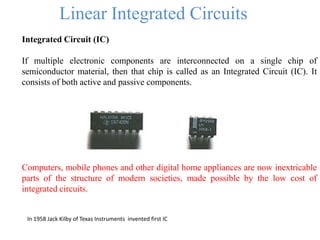
  • 1. Linear Integrated Circuits Integrated Circuit (IC) If multiple electronic components are interconnected on a single chip of semiconductor material, then that chip is called as an Integrated Circuit (IC). It consists of both active and passive components. Computers, mobile phones and other digital home appliances are now inextricable parts of the structure of modern societies, made possible by the low cost of integrated circuits. In 1958 Jack Kilby of Texas Instruments invented first IC
  • 2. Introduction Advantages of Integrated Circuits Integrated circuits offer many advantages. 1. Compact size: For a given functionality, you can obtain a circuit of smaller size using ICs, compared to that built using a discrete circuit. 2. Lesser weight: A circuit built with ICs weighs lesser when compared to the weight of a discrete circuit that is used for implementing the same function of IC. 3. Low power consumption: ICs consume lower power than a traditional circuit, because of their smaller size and construction. 4. Reduced cost: ICs are available at much reduced cost than discrete circuits because of their fabrication technologies and usage of lesser material than discrete circuits. 5. Increased reliability: Since they employ lesser connections, ICs offer increased reliability compared to digital circuits. 6. Improved operating speeds: ICs operate at improved speeds because of their switching speeds and lesser power consumption.
  • 3. Introduction Types of Integrated Circuits Integrated circuits are of two types: •Analog Integrated Circuits •Digital Integrated Circuits Analog Integrated Circuits Integrated circuits that operate over an entire range of continuous values of the signal amplitude are called as Analog Integrated Circuits. Linear Integrated Circuits: An analog IC is said to be Linear, if there exists a linear relation between its voltage and current. IC 741, an 8-pin Dual In-line Package (DIP)op-amp, is an example of Linear IC. Digital Integrated Circuits If the integrated circuits operate only at a few pre-defined levels instead of operating for an entire range of continuous values of the signal amplitude, then those are called as Digital Integrated Circuits.
  • 4. Introduction Pn junction isolation Hybrid circuits Integrated circuits Dielectric isolation Monolithic circuits Bipolar Uni polar MOSFET JFET Classification of ICs Thick &Thin film
  • 5. Introduction Types of ICs Based on the method or techniques used in manufacturing them, types of ICs can be divided into three classes: 1. Thin and thick film ICs: • In thin or thick film ICs, passive components such as resistors, capacitors are integrated but the diodes and transistors are connected as separate components to form a single and a complete circuit. • Thin and thick ICs that are produced commercially are merely the combination of integrated and discrete (separate) components. 2. Monolithic ICs: • In monolithic ICs, the discrete components, the active and the passive and also the interconnections between then are formed on a silicon chip. • The word monolithic is actually derived from two Greek words “mono” meaning one or single and Lithos meaning stone. Thus monolithic circuit is a circuit that is built into a single crystal.
  • 6. Introduction Types of ICs Based on the method or techniques used in manufacturing them, types of ICs can be divided into three classes: 3. Hybrid or Multi chip ICs: • As the name implies, “Multi”, more than one individual chips are interconnected. • The active components that are contained in this kind of ICs are diffused transistors or diodes. The passive components are the diffused resistors or capacitors on a single chip
  • 7. Introduction Chip size and Complexity • Invention of Transistor (Ge) - 1947 • Development of Silicon - 1955-1959 • Silicon Planar Technology - 1959 • First ICs, SSI (3- 30gates/chip) - 1960 • MSI ( 30-300 gates/chip) - 1965-1970 • LSI ( 300-3000 gates/chip) -1970-1975 • VLSI (More than 3k gates/chip) - 1975 • ULSI (more than one million active devices are integrated on single chip)
  • 9. Introduction IC Package types: • Metal can Package • Dual-in-line • Flat Pack Metal can Packages • The metal sealing plane is at the bottom over which the chip is bounded • It is also called transistor pack
  • 10. Introduction IC Package types: • Metal can Package • Dual-in-line • Flat Pack Doul-in-line Package • The chip is mounted inside a plastic or ceramic case • The 8 pin Dip is called MiniDIP and also available with 12, 14, 16, 20pins
  • 11. Introduction IC Package types: • Metal can Package • Dual-in-line • Flat Pack Flat Pack The chip is enclosed in a rectangular ceramic case
  • 12. Introduction Selection of IC Package Type Criteria Metal can package 1. Heat dissipation is important 2. For high power applications like power amplifiers, voltage regulators etc. DIP 1. For experimental or bread boarding purposes as easy to mount 2. If bending or soldering of the leads is not required 3. Suitable for printed circuit boards as lead spacing is more Flat pack 1. More reliability is required 2. Light in weight 3. Suited for airborne applications
  • 13. Introduction Fairchild - µA, µAF National Semiconductor - LM,LH,LF,TBA Motorola - MC,MFC RCA - CA,CD Texas Instruments - SN Signetics - N/S,NE/SE Burr- Brown - BB Manufacturer’s Designation for Linear ICs
  • 14. Introduction 1. Military temperature range : -55o C to +125o C (-55o C to +85o C) 2. Industrial temperature range : -20o C to +85o C (-40o C to +85o C ) 3. Commercial temperature range : 0o C to +70o C (0o C to +75o C ) Temperature Ranges
  • 16. Analog Signal Processing Signal Anything that carries some information is called a signal. A signal is also defined as a physical quantity that varies with time, space or any other independent variable. A signal may be represented in time domain or frequency domain. Human speech is a familiar example of a signal. Electric current and voltage are also examples of signals. System A system is defined as an entity that acts on an input signal and transforms it into an output signal. A system is also defined as a set of elements or fundamental blocks which are connected together and produces an output in response to an input signal. Signal Processing Signal processing is a method of extracting information from the signal which in turn depends on the type of signal and the nature of information it carries.
  • 17. Analog Signal Processing Analog signal processing (ASP) is a signal processing conducted on analog signals by analog means. Analog indicates something that is mathematically represented as a set of continuous values. This differs from digital which uses a series of discrete quantities to represent signal. Analog values are typically represented as a voltage, electric current or electric charge around components in the electronic devices. An error or noise affecting such physical quantities will result in a corresponding error in the signals represented by such physical quantities. Examples of analog signal processing include all sorts of analog active filters, such as crossover filters in loudspeakers, bass, treble and volume controls on stereos, and tint controls on TV‟s. Common analog processing elements include operational amplifiers (Op-Amps), and operational trans-conductance amplifiers (OTA‟s) in addition to passive components.
  • 18. Analog Signal Processing Continuous-Time Signals & Systems A system is considered continuous if the signal exists for all time. Frequently, the terms "analog" and "continuous" are usually employed interchangeably, although they are not strictly the same. Assume a continuous-time system with impulse response h(t), as shown in the following figure. The system processes the continuous-time input signal x(t) in some way, and produces an output y(t). At any value of time, t, we input a value of x(t) into the system and the system produces an output value for y(t). For instance, if we have a multiplier system whose input/output relation is given by y(t) = 7x(t), and the input value x(t) = sin(wt) then the output is y(t) = 7sin(wt).
  • 19. Analog Signal Processing Analog and Digital Signals
  • 20. Digital Signal Processing To perform digitally, there is need for an interface between analog signal and digital processor at input side. This interface is known as an analog to digital (A/D) converter. Similarly, an interface between digital signal and analog processor at output side. This interface is known as an digital to analog (D/A) converter.
  • 21. WHY Analog Signal Processing ? The main disadvantages of DSP are 1. Additional complexity (A/D & D/A Converters) 2. Limit in frequency. High speed AD converters are difficult to achieve in practice. In high frequency applications DSP are not preferred. 3. High cost analog-digital conversion, high power consumption To overcome these drawbacks we prefer analog signal processing Analog signals are processed directly by appropriate analog systems (such as filters or frequency analyzers) or frequency multipliers for the purpose of changing their characteristics or extracting some information.
  • 22. WHY Analog Signal Processing ? The main disadvantages of DSP are 1. Additional complexity (A/D & D/A Converters) 2. Limit in frequency. High speed AD converters are difficult to achieve in practice. In high frequency applications DSP are not preferred. 3. High cost analog-digital conversion, high power consumption To overcome these drawbacks we prefer analog signal processing Analog signals are processed directly by appropriate analog systems (such as filters or frequency analyzers) or frequency multipliers for the purpose of changing their characteristics or extracting some information.
  • 23. Introduction to Operational Amplifier Operational amplifier: Operational amplifier is popularly known as op amp. From its initial application in analog computers to perform mathematical operations such as addition, subtraction, integration, and differentiation, it had the popular name ‘operational amplifier’. 1. Operational amplifiers are used in many industrial, commercial, and consumer electronic gadgets. 2. It is a high gain voltage amplifier. 3. It has many applications such as differential amplifier, voltage comparator, instrumentation amplifier, isolation amplifier (voltage follower for impedance matching application among different stages of amplifiers), and Schmitt trigger applications in waveform generators. 4. Op amp in open-loop configuration functions as a voltage comparator with very large values of gain. Voltage comparator circuits find many applications in Schmitt trigger, etc. 5. Due to the addition of negative feedback to operational amplifier (closed-loop configuration), it has finite values of gain. 6. Operational amplifiers using positive feedback circuit function as oscillator circuits.
  • 24. Introduction to Operational Amplifier The IC is considered as a “black box” device and referred to its schematic structure as in Figure. The general purpose op-amp is of the differential type with both inverting and non- inverting inputs.
  • 25. Block Diagram of an Operational Amplifier An operational amplifier is a multistage amplifier consisting four internal blocks Basic building blocks inside an op amp IC are as follows: 1. First-stage differential amplifier. 2. Second-stage differential amplifier. 3. Voltage-level shifter. 4. Power output stage.
  • 26. Block Diagram of an Operational Amplifier First-Stage differential amplifier It consists of a dual input, balanced output differential amplifier. Its function is to amplify the difference between the two input signals. It provides high differential gain, high input impedance and low output impedance. First stage has two input terminals. It has the facility to operate on two signals working in differential mode of operation. (a) One input is known as ‘inverting (INV) input signal’. (b) Second input is known as ‘non-inverting (NINV) input signal’. Contributes to higher values of common-mode rejection ratio (CMRR). Second-Stage differential amplifier The overall gain requirement of an Op-Amp is very high. Since the input stage alone cannot provide such a high gain. Second stage is used to provide the required additional voltage gain. It consists of another differential amplifier with dual input, and unbalanced (single ended) output.
  • 27. Block Diagram of an Operational Amplifier Voltage level shifting stage As the Op-Amp amplifies even D.C signals, the small D.C. quiescent voltage level of previous stages may get amplified and get applied as the input to the next stage causing distortion the final output. Hence the level shifting stage is used to bring down the D.C. level to ground potential, when no signal is applied at the input terminals. Output stage It consists of a push-pull complementary amplifier which provides large A.C. output voltage swing and high current sourcing and sinking along with low output impedance.
  • 28. BJT Differential Amplifier Differential Amplifier • Amplifies the difference between two voltages applied at its inputs and produces an output voltage. • Rejects the common mode or average of the two input signal voltages. • BJT differential amplifier is one of the building blocks of operational amplifier ICs. • The differential amplifier is also known as difference amplifier. • The differential pair is also known as emitter-coupled pair. Condition for DF Matched transistor are used (properties are same ) Βeta is large (Ic =Ie)
  • 29. BJT Differential Amplifier Working Principles of Differential Amplifier Two identical transistors T1 and T2 are connected in common-emitter transistor operation with symmetrical configuration. Differential amplifier has the provision to connect two input voltages Vin (1) and Vin (2) and obtain two output voltages Vout (1) and Vout (2). The difference between the two output voltages is taken as a single output voltage Vout from the amplifier.
  • 30. BJT Differential Amplifier The circuit is designed for equal biasing voltages VBE1 and VBE2, so that the biasing voltage becomes VBE = 0.7 V for the two identical transistors. Emitter terminals of the two transistors are connected together. The resulting DC bias current IE through RE will be shared equally by the two transistors T1 and T2. Each transistor shares 0.5 IE to contribute to total emitter current IE through the emitter resistor RE The two collector currents IC (1) and IC (2) are equal to 0.5 IC. Each transistor collector current IC = 0.5 IE. Total current IE is the sum of the two DC collector currents of each transistor. The output voltages Vout (1) and Vout (2) are developed at the two collector points, when the input signal voltages are applied.
  • 31. BJT Differential Amplifier The output can be taken from any one of the output terminals and ground. Then, the amplifier operation is single-ended output differential amplifier. The difference of the two output voltages Vout (1) and Vout (2) functions as a single output voltage Vout. Then, it is known as double-ended output arrangement. For a perfectly symmetrical amplifier, the output voltage Vout = AD [Vin (1) - Vin (2)],
  • 33. Main Features of the Differential Amplifier Very large gain occurs when opposite signals are applied to both the input terminals. Difference voltage between the two inputs: Vd = [Vin (1) - Vin (2)] The difference signal Vd is amplified with gain AD. Amplified output voltage (for differential inputs) Vout (D) = AD [Vin (1) - Vin (2)] Very small gain occurs when common type signals are applied to the two input terminals (for common inputs) The overall operation is to amplify the differential signals, while rejecting the common signals at the two inputs. However, total output voltage Vout = Vout (D) + Vout(C)
  • 34. Main Features of the Differential Amplifier Common signals in the amplifier undergo attenuation (due to cancellation) of the noise (unwanted) input signals. This feature is known as common-mode rejection (CMMR). Since the amplification of the opposite signals is much greater than that of the common-mode input signals, the amplifier provides a CMMR. CMRR = AD/AC CMRR(dB) = 20 log10 (AD/AC) Usually, differential amplifiers with larger values of CMRR are used. It measures how well the differential amplifier attenuates or rejects the common- mode signals. The amplifier is virtually free from interfering signals. The signal to noise ratio will be improved by a factor of the value of CMRR.
  • 35. Example Calculate the dc voltages and currents in the circuit of Fig.
  • 36. Example Calculate the dc voltages and currents in the circuit of Fig.
  • 37. JFET Differential Amplifier This is equal to the gain of common source FET amplifier
  • 39. Example In the JFET differential amplifier, gm = 1.41milimhos. Calculate the following: 1. DC output voltage. 2. Gain of single-ended amplifier. 3. Gain of double-ended amplifier.
  • 42. Single-ended Differential Amplifier When one input signal Vin is applied to one of the input terminals of the two transistors, while the second input terminal of the other transistor is grounded, the electronic amplifier is known as single-ended amplifier.
  • 43. Single-ended Differential Amplifier Transistor T1 acts as common-emitter transistor amplifier. Therefore, amplified output voltage Vout (1) of transistor T1 is 180° out-of-phase with input signal voltage. Transistor T2 functions as common base transistor amplifier. Amplified output voltage Vout (2) will be in-phase with input signal Vin.
  • 44. Double-ended Differential Amplifier When two equal input signals Vin (1) and Vin (2) of opposite polarity are applied to the two inputs of differential amplifier, and two outputs are available, the electronic amplifier is known as double-ended differential amplifier The difference between the two equal and opposite polarity input signals is double the magnitude of each signal. Therefore, the amplifier provides large gain.
  • 45. Common-Mode Differential Amplifier When the same input signal is applied to both the input terminals of the two transistors of the differential amplifier, the electronic amplifier is considered to be in common-mode operation of the amplifier. Therefore, the input signals to the two transistors are in-phase and equal in magnitude. The common-mode input signals get cancelled or not amplified by the differential amplifier because it is designed to amplify only the differential signals
  • 46. Why Voltage-level Shifter is used? Voltage-level Shifter (Intermediate Stage Between the Input and the Output Stages) The first two stages of differential amplifiers are DC amplifiers. Therefore, the DC voltage level at the output collector terminal of the second stage will be high. This DC voltage gets propagated to output port along with the AC voltage in normal amplifier chain. It is undesirable. Using DC voltage-level shifter circuit, necessary correction is made to feed it to the input stage of last stage
  • 47. Voltage-level Shifter We begin the analysis by using KVL in the input loop of Figure and letting vin = 0 to obtain Above Equation shows that by varying RE, Vout can be set to any desired dc level (limited to a maximum of VBB–VBE). Since VBB is the dc level acquired from the previous stage, this amplifier is used to shift the level downward (to a lower value). If upward shifting is required, a similar circuit is used but pnp transistors are substituted for the npn transistors.
  • 48. Output Stage of Operational Amplifier 1. It is push–pull complementary symmetry amplifier/Darlington pair amplifier. 2. It has low output impedance Zout. 3. It has large output swing and current carrying capability.
  • 49. Output Stage of Operational Amplifier Darlington pair amplifier.
  • 50. Characteristics of Ideal Op-amp The op-amp is said to be ideal if it has the following characteristics. 1. Infinite voltage gain A. 2. Infinite input resistance Ri. 3. Zero output resistance Ro. 4. Zero output offset. 5. Infinite bandwidth. 6. Infinite common mode rejection ratio. 7. Infinite slew rate.
  • 51. Equivalent circuit of op-amp An Op-Amp can be realized by Thevenin‟s equivalent circuit. Where voltage controlled source AOLVd is an equivalent Thevenin voltage source and R0 is the Thevenin resistance.
  • 52. Various Types of operational amplifiers The very first series of modular solid-state op-amps were introduced by Burr-Brown Research Corporation and G.A. Philbrick Researches Inc. in 1962
  • 53. Internal Blocks of Operational Amplifier IC
  • 54. μA 741 Op-Amp Operational amplifier is an IC. The schematic circuit symbol of op amp is shown in Fig. Op amp (μA 741) is mostly used in the industrial applications and the laboratories in the colleges. Op amp IC has two input terminals, one output terminal, and two supply voltage connection terminals for making circuit connections for applications. There will be some other pins depending upon the IC package. The magnitude of supply voltages and the pin number details of IC are provided in the manufacturer’s data manuals of selected op amp.
  • 55. Pin Configuration of μA 741 Op-Amp Dual-in-line plastic package and metal can package are shown in Figure The DC amplifiers have very large gain operating with two input signal voltages V1 and V2 producing one output voltage Vout. Supply voltages are ± 5 V and ± 15 V.
  • 56. Pin Configuration of μA 741 Op-Amp Pin-1: Offset null terminal. Pin-2: Inverting (INV) input terminal. All input signals connected to this terminal on op amp will appear at the output terminal with 180° phase shift. Pin-3: Non-inverting (N-INV) input terminal. All input signals applied to this terminal on op amp appears as it is in waveform (shape) at the output terminal. Changes occur only in levels of amplitudes at the output voltage. Pin-4: Supply voltage - VCC (negative supply voltage terminal). Pin-5: Offset null terminal. Pin-6: Output terminal; output signal. 1. Output signal will have 180° phase shift to input signals applied to inverting input terminal pin-2. 2. Output signal will be in-phase to input signals applied to non-inverting input terminal pin-3. 3. Output signal depends upon the voltage gain of operational amplifier. Pin-7: supply voltage +VCC terminal (positive supply voltage terminal). Pin-8: no connection.
  • 57. Different types of op amps (a) μA 741 simple and popular type operational amplifier, (b) LT 1056 op amp gas JFET device at its input stage, (c) low power CMOS op amp IC is LMC 660, (d) medium power op amp IC is LM 675, (e) high power operational amplifier IC is LM 12, and (f) LT1220 and LT 1221 are high frequency op amps.
  • 58. Schematic Diagram Of Op-Amp 1. Outside connection from pin-3 is non-inverting (N-NIV) input terminal. V1 is the input voltage at pin-3. 2. +sign at N-NIV terminal indicates that input voltage applied at pin-3 appears at output terminal (6) with zero phase shift. 3. Terminal pin-2 is the inverting (INV) input terminal. V2 is the input voltage at pin- 2. − Sign at INV terminal indicates that the input voltage applied at pin-2 appears at the output terminal (6) with 180° phase shift. 4. Terminal 6 is output terminal (Vout is the output voltage at pin-6).
  • 59. Schematic Diagram Of Op-Amp Differential input voltage: Input voltages V1 and V2 are known as single-ended voltages. All voltages in the operational amplifier are referred with respect to common terminal AC ground. Differential mode voltage VD is the difference between the two input voltages V1 and V2 Therefore, differential input voltage VD = (V1 - V2). Output voltage: Vout = [A (V1 - V2)] = (AVd), where A = amplifier gain. Common-mode voltage: Common-mode input voltage VC is the average value of two input voltages V1 and V2. A very small gain occurs for common inputs. Total (overall) voltage of the operational amplifier due to the presence of differential mode and common-mode input voltages.
  • 60. Characteristic of an Ideal Op-Amp Infinite open-loop gain: If there is no feedback connection between the output and the input terminals of operational amplifier, it is considered to be in open-loop condition. The operational amplifier will have infinite open-loop gain If the gain A is infinite, how are we going to use the op amp? In almost all applications the op amp will not be used alone in a so-called open-loop configuration. Rather, we will use other components to apply feedback to close the loop around the op amp, For 741C it is typically 200,000
  • 61. Characteristic of an Ideal Op-Amp Infinite input resistance Ri: Ideal op-amp offers infinite input resistance and hence the ideal op-amp draws no current (i1=i2=0). For 741C it is of the order of 2MΩ
  • 62. Characteristic of an Ideal Op-Amp Zero output resistance Ro: Ideal op-amp offers zero output resistance so that the output can drive an infinite number of other devices. For op-amp 741 it is 75Ω
  • 63. Characteristic of an Ideal Op-Amp Why high i/p impedance and low o/p impedance We want that the amplified signal does not go any further voltage drop and captures its maximum across Rl
  • 64. Characteristic of an Ideal Op-Amp Zero output offset: The output offset is the output voltage of an amplifier when both inputs are grounded output voltage, when input voltage is zero. Ideal op-amp possesses zero output offset. Infinite bandwidth: An ideal operational amplifier has an infinite frequency response and can amplify any frequency signal from DC to the highest AC frequencies without attenuation. Infinite common mode rejection ratio: Common-mode rejection ratio (CMRR) is defined as the ratio of the differential voltage amplification to the common-mode voltage amplification. For op-amp 741C CMRR is 90 dB
  • 65. Characteristic of an Ideal Op-Amp Infinite slew rate: Slew rate, SR, is the rate of change in the output voltage caused by a step input. Its units are V/μs or V/ms. Higher the slew rate, faster is the op-amp. Ideal Op-Amp has Infinite slew rates so that output voltage changes occur simultaneously with input voltage changes.
  • 67. The Inverting Configuration There are two basic circuit configurations employing an op amp and two resistors: 1. The inverting configuration and 2. The non-inverting configuration Inverting configuration Figure shows the inverting configuration. It consists of one op amp and two resistors R1 and R2. Negative feedback Resistor R2 is connected from the output terminal of the op amp, terminal 3, back to the inverting or negative input terminal If R2 were connected between terminals 3 and 2 we would have called this positive feedback.
  • 68. The Inverting Configuration Closed Loop Gain Closed-loop gain G, is defined as The gain A is very large (ideally infinite). The voltage between the op-amp input terminals should be negligibly small and ideally zero. It follows that the voltage at the inverting input terminal (v1) is given by v1 = v2.
  • 69. The Inverting Configuration Virtual Ground Concept V1= V2 A virtual short circuit means that whatever voltage is at 2 will automatically appear at 1 because of the infinite gain A. Terminal 2 is connected to ground; thus v2 = 0 and v1 = 0. Now we can say that terminal 1 is being a virtual ground—that is, having zero voltage but not physically connected to ground. We say that two input terminals “tracking each other in potential” OR “virtual short circuit” that exists between the two input terminals
  • 70. The Inverting Configuration Analysis The minus sign means that the closed-loop amplifier provides signal inversion.
  • 71. The Inverting Configuration The fact that the closed-loop gain depends entirely on external passive components (resistors R1 and R2) is very significant. It means that we can make the closed-loop gain as accurate as we want by selecting passive components of appropriate accuracy. It also means that the closed-loop gain is (ideally) independent of the op-amp gain. We started out with an amplifier having very large gain A, and through applying negative feedback we have obtained a closed-loop gain R2/R1 that is much smaller than A but is stable and predictable. That is, we are trading gain for accuracy.
  • 72. The Inverting Configuration Effect of Open loop gain: If we denote the output voltage VO, then the voltage between the two input terminals of the op amp will be VO/A. Since the positive input terminal is grounded, the voltage at the negative input terminal must be − VO/A The output voltage VO
  • 73. The Inverting Configuration To minimize the dependence of the closed-loop gain G on the value of the open- loop gain A, we should make Input and Output Resistances: to avoid the loss of signal strength, voltage amplifiers are required to have high input resistance
  • 74. The Inverting Configuration Input and Output Resistances: In the case of the inverting op-amp configuration we are studying, to make Ri high we should select a high value for R1. However, if the required gain R2/R1 is also high, then R2 could become impractically large (e.g., greater than a few megohms). We may conclude that the inverting configuration suffers from a low input resistance
  • 75. Example Assuming the op amp to be ideal, derive an expression for the closed-loop gain VO/VI of the circuit shown in Fig. Use this circuit to design an inverting amplifier with a gain of 100 and an input resistance of 1M. Assume that for practical reasons it is required not to use resistors greater than 1 M.
  • 76. Example Assuming the op amp to be ideal, derive an expression for the closed-loop gain VO/VI of the circuit shown in Fig. Use this circuit to design an inverting amplifier with a gain of 100 and an input resistance of 1MΩ. Assume that for practical reasons it is required not to use resistors greater than 1 M Ω.
  • 78. Example Now, since an input resistance of 1 M Ω is required, we select R1 = 1M Ω. Then, with the limitation of using resistors no greater than 1M Ω, the maximum value possible for the first factor in the gain expression is 1 and is obtained by selecting R2 =1M Ω. To obtain a gain of −100, R3 and R4 must be selected so that the second factor in the gain expression is 100. If we select the maximum allowed (in this example) value of 1 M for R4, then the required value of R3 can be calculated to be 10.2 k Ω.
  • 79. The Weighted Summer A very important application of the inverting configuration is the weighted-summer circuit shown in Fig. Here we have a resistance Rf in the negative-feedback path (as before), but we have a number of input signals v1,v2, . . . ,vn each applied to a corresponding resistor R1,R2, . . . ,Rn, which are connected to the inverting terminal of the op amp.
  • 80. The Weighted Summer The output voltage Vo That is, the output voltage is a weighted sum of the input signals v1,v2, . . . ,vn. This circuit is therefore called a weighted summer. Note that each summing coefficient may be independently adjusted by adjusting the corresponding “feed-in” resistor (R1 to Rn).
  • 81. The Weighted Summer Weighted summers are utilized in a variety of applications including in the design of audio systems, where they can be used in mixing signals originating from different musical instruments.
  • 82. The Non-Inverting Configuration In this configuration the input signal VI is applied directly to the positive input terminal of the op amp while one terminal of R1 is connected to ground. The Closed-Loop Gain Assuming that the op amp is ideal with infinite gain, a virtual short circuit exists between its two input terminals. Hence the difference input signal is
  • 84. The Non-Inverting Configuration The current into the op-amp inverting input is zero, the circuit composed of R1 and R2 acts in effect as a voltage divider feeding a fraction of the output voltage back to the inverting input terminal of the op amp; that is, Then the infinite op-amp gain and the resulting virtual short circuit between the two input terminals of the op amp forces this voltage to be equal to that applied at the positive input terminal; thus,
  • 85. The Non-Inverting Configuration Degenerative feedback Let VI increase. Such a change in VI will cause VID to increase, and VO will correspondingly increase as a result of the high (ideally infinite) gain of the op amp. However, a fraction of the increase in VO will be fed back to the inverting input terminal of the op amp through the (R1,R2) voltage divider. The result of this feedback will be to counteract the increase in VID, driving VID back to zero, albeit at a higher value of VO that corresponds to the increased value of VI. This degenerative action of negative feedback gives it the alternative name degenerative feedback.
  • 86. The Non-Inverting Configuration Effect of Finite Open-loop Gain Vo = A (VI- Vx) » Vx = VI –Vo/A I2=I1 (Vo-Vx)/R2 = Vx/R1 R1 (Vo-Vx) = VxR2 R1 (Vo-VI-Vo/A)= R2 (VI –Vo/A) Vo(1+ 1/A(1+R2/R1)) = VI (1+R2/R1) Vx
  • 87. The Non-Inverting Configuration The gain expression in the above equation reduces to the ideal value for A=∞. In fact, it approximates the ideal value for The expressions for the actual and ideal values of the closed-loop gain G in above Eqs., can be used to determine the percentage error in G resulting from the finite op- amp gain A as
  • 88. The Non-Inverting Configuration Effect of finite loop gain on Input Resistance Rin Apply KCL at node a Rdi differential resistance a V1 Rdi Vi
  • 90. The Non-Inverting Configuration An increase in the value of input resistance leads to an improved performance of the operational amplifier with feedback.
  • 91. The Non-Inverting Configuration Effect of finite loop gain on output Resistance Rout Apply KCL at node a
  • 92. The Non-Inverting Configuration The effect of finite open loop gain of the operational amplifier on the output resistance of non-inverting amplifiers clearly indicates that the output resistance decreases to a very low value. The typical value of output resistance of an operational amplifier is 75Ω. For an open loop gain of 1000, output resistance reduces to less than 1Ω. In most of the applications it enhances the overall performance of the operational amplifier.
  • 93. Example 1. Calculate the voltage gain of an inverting op amp with R1 = 3.3 kΩ and resistor R2 = 33 kΩ. 2. Calculate the output voltage when the input voltage = 0.5 V. Solution:
  • 94. Example 1. Calculate the voltage gain of non-inverting op amp if R1 = 2.2 kΩ and resistor R2 = 22 kΩ 2. Calculate output voltage for input voltage of 0.2 V. Solution:
  • 95. Example 1. Calculate the voltage gain of non-inverting op amp if R1 = 2.2 kΩ and resistor R2 = 22 kΩ 2. Calculate output voltage for input voltage of 0.2 V. Solution:
  • 96. Voltage Follower The property of high input impedance is a very desirable feature of the noninverting configuration. It enables using this circuit as a buffer amplifier to connect a source with a high impedance to a low-impedance load In many applications the buffer amplifier is not required to provide any voltage gain; rather, it is used mainly as an impedance transformer or a power amplifier. In such cases we may make R2 = 0 and R1 =∞to obtain the unity-gain amplifier This circuit is commonly referred to as a voltage follower, since the output • g follows the input. In the ideal case, vO =vI ,Rin = ∞ , Rout =0 In the voltage-follower circuit the entire output is fed back to the inverting input, the circuit is said to have 100% negative feedback
  • 97. Integrators and Differentiators Till now we utilized resistors in the op-amp feedback path and in connecting the signal source to the circuit, that is, in the feed-in path. As a result, circuit operation has been (ideally) independent of frequency. By allowing the use of capacitors together with resistors in the feedback and feed- in paths of op-amp circuits, we open the door to a very wide range of useful and exciting applications of the op amp. We begin our study of op-amp–RC circuits by considering two basic applications, namely, signal integrators and differentiators.
  • 98. Integrators and Differentiators The Inverting Configuration with General Impedances The closed-loop transfer function or closed loop gain
  • 99. Integrator A circuit in which the output voltage waveform is the time integral of the input voltage waveform is called integrator or integrating amplifier. The expression for the output voltage Vo(t) can be obtained by writing Kirchhoff ’s current equation at node a as given by
  • 101. The Inverting Integrator where vo(0) is the integration constant and is proportional to the value of the output voltage vo(t) at t = 0. Above Equation indicates that the output voltage is directly proportional to the negative integral of the input voltage and inversely proportional to the time constant R1Cf . Thus the circuit provides an output voltage that is proportional to the time integral of the input, with VC being the initial condition of integration and CR the integrator time constant. There is a negative sign attached to the output voltage, and thus this integrator circuit is said to be an inverting integrator.
  • 102. The Inverting Integrator The operation of the integrator circuit can be described alternatively in the frequency domain by substituting Z1(s)=R and Z2(s)=1/sC in above equation
  • 103. The Inverting Integrator The frequency ωint is known as the integrator frequency and is simply the inverse of the integrator time constant. the feedback element is a capacitor, and thus at dc, where the capacitor behaves as an open circuit, there is no negative feedback! This is a very significant observation and one that indicates a source of problems with the integrator circuit: Any tiny dc component in the input signal will theoretically produce an infinite output. No infinite output voltage results in practice
  • 104. The Inverting Integrator The dc problem of the integrator circuit can be alleviated by connecting a resistor RF across the integrator capacitor C The gain at dc will be –RF/R rather than infinite Such a resistor provides a dc feedback path. Unfortunately, however, the integration is no longer ideal, and the lower the value of RF, the less ideal the integrator circuit becomes. This is because RF causes the frequency of the integrator pole to move from its ideal location at ω =0 to one determined by the corner frequency of the STC network (RF,C). Now, the integrator transfer function becomes
  • 105. The Inverting Integrator The ideal function of −1/sCR The lower the value we select for RF, the higher the corner frequency (1/CRF) will be and the more non-ideal the integrator becomes. Thus selecting a value for RF presents the designer with a trade-off between dc performance and signal performance.
  • 106. Example Find the output produced by a Miller integrator in response to an input pulse of 1- V height and 1-ms width. Let R = 10 kΩ and C = 10 nF. If the integrator capacitor is shunted by a 1M Ω resistor, how will the response be modified? For C =10 nF and R=10 KΩ, CR = 0.1 ms, It reaches a magnitude of −10 V at t = 1 ms and remains constant thereafter.
  • 107. Example The 1-V input pulse produces a constant current through the capacitor of 1 V/10 KΩ=0.1 mA. This constant current I =0.1 mA supplies the capacitor with a charge It, and thus the capacitor voltage changes linearly as (It/C), resulting in VO =−(I/C)t. Now we consider the situation with resistor RF =1 MΩ connected across C The exponential will be interrupted at the end of the pulse, that is, at t = 1 ms, and the output will reach the value
  • 108. Summing Integrator Circuit By adding multiple input voltages V1, V2, V3 … Vn to an integrator circuit, ‘summing integrator circuit’ can be realized, which is similar to an ordinary summing amplifier.
  • 109. Application of Integrator 1. Generation of sweep and ramp voltages (wave-shaping circuits). 2. Filter circuits. 3. Analog computers. 4. Control systems. 5. Computer simulation of mathematical functions. 6. Analog to digital converters. 7. Pulse width modulator with active integrator.
  • 110. The Op-Amp Differentiator Interchanging the location of the capacitor and the resistor of the integrator circuit results a differentiator OR
  • 111. The Op-Amp Differentiator In frequency-domain transfer function of the differentiator circuit
  • 112. The Op-Amp Differentiator Gain of differentiator circuit Input impedance (1/wc) is decreases with increase frequency, thereby making the circuit sensitive to high frequency noise
  • 115. Summing Differentiator Similar to summing amplifier, summing differentiator works with multiple inputs
  • 116. Applications of Differentiator 1. Analog computer calculations. 2. Process controls that monitor the changing conditions. 3. De-bouncing of switch contacts in logic applications. 4. High pass filter circuits (active filter circuits).
  • 117. Example Design a differentiator using op-amp to differentiate an input signal with fmax = 200 Hz
  • 118. Difference Amplifiers A difference amplifier is one that responds to the difference between the two signals applied at its input and ideally rejects signals that are common to the two inputs Ideally the difference amplifier will amplify only the differential input signal VId and reject completely the common-mode input signal VIcm, practical circuits will have an output voltage VO given by The efficacy of a differential amplifier is measured by the degree of its rejection of common-mode signals in preference to differential signals.
  • 119. A Single-Op-Amp Difference Amplifier The gain of the non-inverting amplifier configuration is positive, (1 + R2/R1), while that of the inverting configuration is negative, (−R2/R1). Combining the two configurations together is we , getting the difference between two input signals. 3 3 3 2 3 2 3 3 2
  • 120. A Single-Op-Amp Difference Amplifier When resistors, R1 = R3 and R2 = R4 the above transfer function for the differential amplifier can be simplified to the following expression: 3 2 2
  • 121. A Single-Op-Amp Difference Amplifier Now consider the circuit with only a common-mode signal applied at the input
  • 122. A Single-Op-Amp Difference Amplifier For the design with the resistor ratios selected as expected. Note, however, that any mismatch in the resistance ratios can make Acm nonzero, and hence CMRR finite.
  • 123. A Single-Op-Amp Difference Amplifier In addition to rejecting common-mode signals, a difference amplifier is usually required to have a high input resistance. To find the input resistance between the two input terminals (i.e., the resistance seen by VId), called the differential input resistance Rid . Here we have assumed that the resistors are selected so that R3 = R1 and R4 = R2 Note that if the amplifier is required to have a large differential gain (R2/R1), then R1 of necessity will be relatively small and the input resistance will be correspondingly low, a drawback of this circuit. Another drawback of the circuit is that it is not easy to vary the differential gain of the amplifier.
  • 124. The Instrumentation Amplifier An instrumentation amplifier is a device that amplifies the difference between the voltages at its two input terminals and hence known as differential voltage gain amplifier. This amplifier can be used for accurate and low signal amplification of signals with the common mode input. The instrumentation amplifier has the characteristics such as High input impedance Low output impedance High Common Mode Rejection Ratio (CMRR) Low output offset (dc offset) and High gain stability It can be used for the applications that include data acquisition systems where high common mode noise dominates, measurement of physical quantities such as temperature, humidity, bio signal measurement and optical signal intensity measurements.
  • 125. The Instrumentation Amplifier It consists of two stages in cascade. The first stage is formed by op amps A1 and A2 and their associated resistors, and the second stage is the by-now-familiar difference amplifier formed by op amp A3 and its four associated resistors.
  • 126. The Instrumentation Amplifier The difference amplifier in the second stage operates on the difference signal (1+R2/R1)(VI2 −VI1) = (1+R2/R1)VId and provides at its output
  • 127. The Instrumentation Amplifier The circuit in Figure has the advantage of very high (ideally infinite) input resistance and high differential gain.
  • 128. The Instrumentation Amplifier The circuit, however, has three major disadvantages: 1. The input common-mode signal VIcm is amplified in the first stage by a gain equal to that experienced by the differential signal VId . 2. The two amplifier channels in the first stage have to be perfectly matched, otherwise a spurious signal may appear between their two outputs. Such a signal would get amplified by the difference amplifier in the second stage. 3. To vary the differential gain Ad , two resistors have to be varied simultaneously, say the two resistors labelled R1. At each gain setting the two resistors have to be perfectly matched: a difficult task.
  • 129. The Instrumentation Amplifier All three problems can be solved with a very simple wiring change: Simply disconnect the node between the two resistors labelled R1, node X, from ground. And two resistors (R1 and R1) together into a single resistor (2R1).
  • 132. The Instrumentation Amplifier Observe that proper differential operation does not depend on the matching of the two resistors labeled R2. Indeed, if one of the two is of different value, say R 2, the expression for Ad becomes If the two input terminals are connected together to a common-mode input voltage vIcm. It is easy to see that an equal voltage appears at the negative input terminals of A1 and A2, causing the current through 2R1 to be zero. Thus there will be no current flowing in the R2 resistors, and the voltages at the output terminals of A1 and A2 will be equal to the input (i.e., VIcm). Thus the first stage no longer amplifies VIcm; it simply propagates VIcm to its two output terminals, where they are subtracted to produce a zero common-mode output by A3.
  • 133. DC Imperfections An ideal operational amplifier draws no current from the signal source and its response is independent of the temperature variations. However, a practical op-amp gets affected by the environmental and process parameter variations. The non-ideal dc characteristics of the op-amp are (i) Input bias current (ii) Input offset current (iii) Input offset voltage and (iv) Thermal drift
  • 134. Input bias current The input bias current is the average of the currents that flow into the inverting and non-inverting input terminals of an op-amp. The average value IB is called the input bias current Typical values for general-purpose op amps that use bipolar transistors are IB = 100 nA Though both the transistors are identical, the two currents IB1 and IB2 are not exactly equal. This is due to the internal imbalances created during the fabrication process. Therefore, the manufacturers specify the input bias current IB as the average of the two base currents
  • 135. Input bias current The non-inverting input terminal of the op-amp is grounded. For this circuit, the output voltage Vo must be 0 V. However, the output voltage is found to be offset by a value of
  • 136. Input bias current To overcome this issue compensation resistor Rcomp is introduced in the non- inverting terminal path to ground. The current IB1 flowing through the compensating resistor Rcomp develops a voltage Vcomp across it By choosing the proper value of Rcomp to get V2 = Vcomp cancels the offset effect, thus making the output Vo = 0.
  • 137. Input bias current For offset compensation, we know Vo must be zero for Vi = 0. we must have V2 = Vcomp
  • 138. Input bias current The compensating resistor Rcomp must be equal to the parallel combination of input and feedback resistors R1 and Rf connected at the inverting input terminal of the op-amp.
  • 139. Input offset current The difference in magnitude between IB1 and IB2 is called input offset current IOS. The manufacturers specify IOS for a circuit when the output Vo is zero and temperature is 25°C. IOS is typically less than 25% of IB for the average input bias current. It is 200nA for BJT op-amp and 10pA for FET op-amp. Applying KCL at node a
  • 140. Input offset current The output voltage due to offset current IOS is dependent on the feedback resistor Rf, and it can be a positive or negative dc voltage with respect to ground. Normally IOS << IB, the output offset caused by IOS is much smaller than that caused by IB.
  • 141. Example Assume that an op-amp has IB1 = 400 nA and IB2 = 300 nA. Determine the average bias current IB and the offset current IOS. Solution:
  • 142. Input offset Voltage Input offset voltage VOS is the differential input voltage that exists between the inverting and non-inverting input terminals of an op-amp. In other words, this can be defined as the voltage that is to be applied between the two input terminals for making the output voltage zero. Figure shows the op-amp with input offset voltage VOS applied at the non- inverting terminal.
  • 143. Input offset Voltage At the node a,
  • 144. Total Output offset voltage The total output offset voltage VOT can be due to either the input bias current or the input offset voltage, and also, it can be either positive or negative with respect to ground. when Rcomp is connected in the circuit, then the total output offset voltage will be Since IOS < IB, it can be seen that the use of Rcomp ensures a reduction in the output offset voltage generated due to bias current.
  • 145. Example Assume that Rf = 10 KΩ, R1 = 2 KΩ , input offset voltage VOS = 5 mV, input offset current IOS = 50 nA(max) and input bias current IB = 200 nA(max) at TA = 25°C. Determine the maximum output offset voltage with and without Rcomp. Solution:
  • 146. Thermal Drift It was assumed so far that the parameters VOS, IB and IOS are constant for a given op-amp. But in practice, the following operating conditions pose a great challenge to these parameters: (i) Change in temperature ΔT (ii) Change in supply voltage and (iii) Change in time The change in temperature causes the most serious variation in the values of VOS, IB and IOS. The term thermal drift is used to identify such changes and it is defined as the average rate of change of input offset voltage per unit change in temperature.
  • 147. Example At room temperature 25°C. If the temperature is raised to 75°C, determine the maximum change in output voltage due to (a) drift in VOS and (b) drift in IOS.
  • 148. Example At room temperature 25°C. If the temperature is raised to 75°C, determine the maximum change in output voltage due to (a) drift in VOS and (b) drift in IOS.
  • 151. Frequency Response The gain of the op-amp is assumed a constant for dc and very low frequencies of operation. However, it is observed in practice that the gain is a complex number and a function of frequency. At a given frequency, the gain A has a certain magnitude and a phase angle. Any change in operating frequency causes variation in gain magnitude and phase angle. Therefore, frequency response is defined as the manner in which, the gain of the op-amp responds to different frequencies. Ideally, an op-amp is expected to have an infinite bandwidth. If the open-loop gain is specified as a particular value, it must remain the same throughout the audio and high radio frequency ranges. However, the gain of a practical op-amp decreases or rolls-off at higher frequencies.
  • 152. Frequency Response The decreasing gain of the op-amp can be attributed to a capacitive component included in the equivalent circuit of the op-amp. Two major sources can be considered responsible for this capacitive component. (i) Due to BJTs and FETs junction capacitors. The junction capacitors are very small, of the order of picofarads and they act as open-circuits at low frequencies and as reactive paths at higher frequencies. (ii) The internal construction of the op-amp with transistors, resistors and capacitors integrated on the same substrate introduce parasitic or stray capacitances, wherever two conducting paths are found separated by insulator, which, in effect, creates a capacitor
  • 153. Frequency Response The combined effect of these capacitances reduces the gain of op-amp at high frequencies. The high frequency model of an op-amp with only one break frequency and all the capacitor effects represented by a single capacitor C is shown in figure
  • 154. Frequency Response Open Loop gain as a function of frequency where A is the open-loop voltage gain as a function of frequency and f1 is the break frequency or the dominant-pole frequency of the op-amp and A0 is the voltage gain of the op-amp at 0 Hz (dc) or the low frequency open-loop gain.
  • 155. Frequency Response Open Loop gain as a function of frequency Above equation indicates that the open-loop gain A is a complex quantity dependent on operating frequency. The magnitude of open-loop gain is
  • 156. Frequency Response Open Loop gain as a function of frequency (i) The open-loop gain A is approximately constant from 0 Hz to break frequency f1. (ii) When f = f1, the gain A is 3 dB down from its value at 0 Hz. Hence, the break frequency is called –3 dB frequency or corner frequency. (iii) For f > f1, the open-loop gain rolls-off at a rate of –20 dB/decade or – 6 dB/octave. (iv) At a particular input frequency fT shown, the open-loop gain A is unity, or gain in dB is zero. This is called the unity gain bandwidth, small-signal bandwidth and unity gain cross-over frequency. The unity gain-bandwidth of IC 741C is approximately 1 MHz. v) The phase angle is zero at f = 0, and at f = f1, the phase angle is –45° (lagging) and at infinite frequency, the phase angle is –90°.
  • 157. Frequency Response Open Loop gain as a function of frequency The voltage transfer function for a single stage is expressed by However, a practical op-amp has a number of stages and each stage contributes for a capacitive component. Therefore, due to a number of RC pole pairs, there will be an equal number of different corner frequencies. Therefore, the transfer function of an op-amp with three break frequencies can be written as
  • 158. Frequency Response Open Loop gain as a function of frequency As frequency increases, the cascading effect of RC pairs or poles takes effect and correspondingly, the roll-off rate increases successively by –20 dB/decade at each of the corner frequencies.
  • 159. Frequency Response Open Loop gain as a function of frequency The specification sheets normally present (i) manufacturer’s plot of open-loop gain A versus frequency, with the point funity indicating the frequency where A = 1 (ii) specification called transient response time (unity gain), which is typically 0.25 ms and 0.8 ms at maximum for 741 op-amp. The bandwidth BW is determined from the rise time specification by using the relation The small signal unity gain-bandwidth characteristic is an important parameter of an op-amp. For an op-amp with a single break frequency f1, the gain-bandwidth product is constant and it can be written as
  • 160. Frequency Response Bandwidth with feedback The bandwidth of an amplifier is defined as the range of frequencies within which the gain remains constant. The gain-bandwidth product of an op-amp is always constant. The gain of an op-amp and its bandwidth are inversely proportional to one another. The bandwidth of an op-amp can be increased by providing feedback signal to its input. The product of closed-loop gain Av and closed-loop bandwidth BWCL is same as the product of open-loop gain and open-loop bandwidth.
  • 161. Example An op-amp has a unity gain-bandwidth of 1.5 MHz. For a signal of frequency 2 kHz, what is the openloop dc voltage gain?
  • 162. Frequency Compensation When wider bandwidth and limited closed-loop gain are required, suitable compensation techniques are employed. The two types of compensation techniques used in practice are (i) External frequency compensation and (ii) Internal frequency compensation External frequency compensation The compensating network is connected externally to the op-amp for modifying the response suiting the requirements. The compensating network alters the response so that –20 dB/decade of roll-off rate is achieved over a broad range of frequency.
  • 163. Example Calculate (a) voltage gain (b) output voltage (c) load current IL
  • 164. Slew Rate Slew rate is an important parameter which limits the bandwidth for large signals and it indicates how fast its output voltage can change. It is defined as the maximum rate of change of output voltage realised by a step input voltage, and it is usually specified in units of V/μs. The slew rate of the op-amp is related to its frequency response. The op-amps with wide bandwidth have better slew rates. Slew rate limiting affects all amplifiers where capacitance on internal nodes, or as part of the external load, has to be charged and discharged as voltage levels vary. The general purpose op-amps such as the 741 have a maximum slew rate of 0.5 V/μs, which means that the output voltage can change at a maximum of 0.5 V in 1 μs.
  • 165. Slew Rate The slew rate (SR) of the op amp and is defined as
  • 166. Slew Rate The capacitor within or outside the op-amp is required to prevent oscillation and this capacitor restricts the response of op-amp to a rapidly changing input signal. The rate at which the voltage across the capacitor Vc increases is given by where I is the current furnished by the internal circuit. This means that the op-amp must have either a higher current or a small compensation capacitor. For example, the IC 741 can provide 15 mA of maximum current to its internal 30 pF capacitor. That is,
  • 167. Slew Rate Slew rate limiting of sine-wave The slew rate limits the speed of response of all the large signal wave-shapes. Figure shows vi as a large amplitude, high frequency sine-wave with a peak amplitude of Vm.
  • 168. Slew Rate The maximum frequency fmax at which an undistorted output voltage with a peak value Vm can be obtained is determined by The maximum peak sinusoidal output voltage Vm(max) that can be obtained at a frequency of f is given by
  • 169. Example Assume that an op-amp 741 connected as a unit gain inverting amplifier is applied with an input change of 10 V. Determine the time taken for the output to change by 10 V.
  • 170. Example Assuming slew rate for 741 is 0.5 V/μs, what is the maximum undistorted sine-wave that can be obtained for (a) 12V peak and (b) 2V peak?
  • 171. Example IC 741 is used as an inverting amplifier with a gain of 100. The voltage gain Vs frequency characteristic is flat up to 10 kHz. Determine the maximum peak-to-peak input signal that can be applied without any distortion to the output.
  • 172. Example The 741C is used as an inverting amplifier with a gain of 50. The sinusoidal input signal has a variable frequency and maximum amplitude of 20 mV peak. What is the maximum frequency of the input at which the output will be undistorted? Assume that the amplifier is initially nulled.
  • 173. Effect of Finite Open-Loop Gain and Bandwidth on Circuit Performance Frequency Dependence of the Open-Loop Gain The differential open-loop gain A of an op amp is not infinite; rather, it is finite and decreases with frequency.
  • 174. Effect of Finite Open-Loop Gain and Bandwidth on Circuit Performance The uniform –20-dB/decade gain rolloff shown is typical of internally compensated op amps. These are units that have a network (usually a single capacitor) included within the same IC chip whose function is to cause the op-amp gain to have the single-time-constant (STC) low-pass response shown. This process of modifying the open- loop gain is termed frequency compensation, and its purpose is to ensure that op-amp circuits will be stable (as opposed to oscillatory).
  • 175. Effect of Finite Open-Loop Gain and Bandwidth on Circuit Performance The gain A(s) of an internally compensated op amp may be expressed as where A0 denotes the dc gain and ωb is the 3-dB frequency (corner frequency or “break” frequency).
  • 176. Effect of Finite Open-Loop Gain and Bandwidth on Circuit Performance The gain |A| reaches unity (0 dB) at a frequency denoted by ωt and given by
  • 177. Effect of Finite Open-Loop Gain and Bandwidth on Circuit Performance Since ft is the product of the dc gain A0 and the 3-dB bandwidth fb (where fb =ωb/2π), it is also known as the gain–bandwidth product (GB) The frequency ft =ωt/2π is known as the unity-gain bandwidth for ω >>ωb the open-loop gain The gain magnitude can be obtained
  • 178. Effect of Finite Open-Loop Gain and Bandwidth on Circuit Performance As a matter of practical importance, we note that the production spread in the value of ft between op-amp units of the same type is usually much smaller than that observed for A0 and fb. For this reason ft is preferred as a specification parameter. Finally, it should be mentioned that an op amp having this uniform –6-dB/octave (or equivalently –20- dB/decade) gain rolloff is said to have a single-pole model. Also, since this single pole dominates the amplifier frequency response, it is called a dominant pole.
  • 179. Effect of Finite Open-Loop Gain and Bandwidth on Circuit Performance Frequency Response of Closed-Loop Amplifiers (Inverting) If we denote the output voltage vO, then the voltage between the two input terminals of the op amp will be vO/A. Since the positive input terminal is grounded, the voltage at the negative input terminal must be −vO/A. The current i1 through R1 can now be found from The infinite input impedance of the op amp forces the current i1 to flow entirely through R2. The output voltage vO can thus be determined from
  • 180. Effect of Finite Open-Loop Gain and Bandwidth on Circuit Performance Frequency Response of Closed-Loop Amplifiers
  • 181. Effect of Finite Open-Loop Gain and Bandwidth on Circuit Performance Frequency Response of Closed-Loop Amplifiers The closed-loop gain rolls off at a uniform –20-dB/decade slope with a corner frequency (3-dB frequency) given by
  • 182. Effect of Finite Open-Loop Gain and Bandwidth on Circuit Performance Frequency Response of Closed-Loop Amplifiers (Non Inverting) Thus the noninverting amplifier has an STC low-pass response with a dc gain of (1+R2/R1) and a 3-dB frequency A finite open-loop gain A, yields the closed-loop transfer function
  • 183. Example The circuit of Figure uses an op amp that is ideal except for having a finite gain A. Measurements indicate vO =4.0 V when vI = 1.0 V. What is the op-amp gain A? V+ = V1 (1k /(1M+IK)) = 1/1001 V0/V+ = A A = 4004
  • 184. Example Consider an op amp that is ideal except that its open-loop gain A=1000. The op amp is used in a feedback circuit, and the voltages appearing at two of its three signal terminals are measured. In each of the following cases, use the measured values to find the expected value of the voltage at the third terminal. Also give the differential and common-mode input signals in each case. (a) v2 = 0 V and v3 = 2 V; (b) v2 =+5 V and v3 =−10 V; (c) v1 = 1.002 V and v2 = 0.998 V. Solution (a) (b) (c)
  • 186. Example The internal circuit of a particular op amp can be modeled by the circuit shown in Figure. Express v3 as a function of v1 and v2. For the case Gm = 10 mA/V, R = 10 KΩ, and μ = 100, find the value of the open-loop gain A. Comparing with general expression of Opamp
  • 187. Example Use the circuit of Figure to design an inverting amplifier having a gain of−10 and an input resistance of 100 KΩ. Give the values of R1 and R2.
  • 188. Example For the circuit in Figure determine the values of v1, i1, i2,vO, iL, and iO. Also determine the voltage gain vO/vI , current gain iL/iI , and power gain PO/PI .
  • 189. Example Design an inverting op-amp circuit to form the weighted sum vO of two inputs v1 and v2. It is required that vO =−(v1 +5v2). Choose values for R1, R2, and Rf so that for a maximum output voltage of 10 V the current in the feedback resistor will not exceed 1 mA.
  • 190. Example Use the superposition principle to find the output voltage of the circuit shown in Figure. When V2 =0 When V1 = 0
  • 191. Example Consider the difference-amplifier circuit of Figure for the case R1=R3=2 kΩ and R2 =R4 =200 kΩ. (a) Find the value of the differential gain Ad . (b) Find the value of the differential input resistance Rid and the output resistance Ro. (c) If the resistors have 1% tolerance (i.e., each can be within ±1% of its nominal value), find the worst-case common-mode gain Acm and hence the corresponding value of CMRR.
  • 192. Example Consider the difference-amplifier circuit of Figure for the case R1=R3=2 kΩ and R2 =R4 =200 kΩ. (a) Find the value of the differential gain Ad . (b) Find the value of the differential input resistance Rid and the output resistance Ro. (c) If the resistors have 1% tolerance (i.e., each can be within ±1% of its nominal value), find the worst-case common-mode gain Acm and hence the corresponding value of CMRR.
  • 193. Example Find values for the resistances in the circuit of Figure so that the circuit behaves as a difference amplifier with an input resistance of 20 KΩ and a gain of 10.
  • 194. Example Consider a symmetrical square wave of 20-V peak-to-peak, 0 average, and 2-ms period applied to a integrator. Find the value of the time constant CR such that the triangular waveform at the output has a 20-V peak-to-peak amplitude. When V1 = +10v the current through the capacitor will be in the direction indicated i=10V/R and the output voltage will decreases linearly from -10V to 10V. In T/2 seconds the capacitor voltage changes by20V
  • 195. Example Use an ideal op amp to design an inverting integrator with an input resistance of 10 KΩ and an integration time constant of 10^−3 s. What is the gain magnitude and phase angle of this circuit at 10 rad/s? What is the frequency at which the gain magnitude is unity?
  • 196. Example Consider an inverting amplifier circuit designed using an op amp and two resistors, R1 = 10 k and R2 =1M. If the op amp is specified to have an input bias current of 100 nA and an input offset current of 10 nA, find the output dc offset voltage resulting and the value of a resistor R3 to be placed in series with the positive input lead in order to minimize the output offset voltage. What is the new value of VO?
  • 197. Example Consider a Miller integrator with a time constant of 1 ms and an input resistance of 10 k. Let the op amp have VOS = 2 mV and output saturation voltages of ± 12 (a) Assuming that when the power supply is turned on the capacitor voltage is zero, how long does it take for the amplifier to saturate? (b) Select the largest possible value for a feedback resistor RF so that at least ±10 V of output signal swing remains available. What is the corner frequency of the resulting STC network?
  • 198. Example Consider a Miller integrator with a time constant of 1 ms and an input resistance of 10 k. Let the op amp have VOS = 2 mV and output saturation voltages of ± 12 (a) Assuming that when the power supply is turned on the capacitor voltage is zero, how long does it take for the amplifier to saturate? (b) Select the largest possible value for a feedback resistor RF so that at least ±10 V of output signal swing remains available. What is the corner frequency of the resulting STC network?
  • 199. Example An internally compensated op amp is specified to have an open-loop dc gain of 106 dB and a unity-gain bandwidth of 3 MHz. Find fb and the open-loop gain (in dB) at fb, 300 Hz and 3 kHz.