The World of Wafer Inspection A Pinnacle of Precision
1. The World of Wafer Inspection A Pinnacle of Precision
In the realm of cutting-edge technology, where microelectronics reign supreme, the quality and
integrity of silicon wafers are paramount. These wafer-thin substrates are the unsung heroes
behind our beloved electronic devices, providing the foundation for everything from
microprocessors to memory chips. Ensuring their flawless perfection is no easy task, and this is
where Wafer Inspection comes into play, especially in the bustling hub of California.
The Heart of Silicon Valley:
California, often dubbed the "Golden State," is renowned as the global epicenter of technology
innovation. It's home to Silicon Valley, the birthplace of many tech giants, and a breeding ground
for startups. The state's relentless pursuit of technological advancement has led to the evolution
of various industries, and the semiconductor industry is no exception.
Wafer Inspection, an integral part of semiconductor manufacturing, is a crucial component in
maintaining California's technological dominance. The embarks on a journey to explore the
nuances of Wafer Inspection, its significance, and the cutting-edge technologies driving it forward
in the Californian semiconductor landscape.
The Essence of Wafer Inspection:
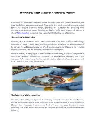
Wafer Inspection is the pivotal process of scrutinizing semiconductor wafers for imperfections,
defects, and irregularities that could potentially hinder the performance of integrated circuits
(ICs) or other microelectronic components. Think of it as a microscopic detective, tirelessly
examining each wafer to ensure it meets the stringent standards set by the semiconductor
industry.
2. The Imperceptible Culprits Defects:
Before delving deeper into Wafer Inspection, it's essential to understand the nemesis it seeks to
conquer – defects. These microscopic villains, often lurking unseen to the naked eye, can wreak
havoc in the world of semiconductors. There are various types of defects, including:
• Particles and Contaminants
These tiny intruders can find their way onto the wafer during the manufacturing process. Even
the smallest speck of dust can disrupt the precise patterns etched into the wafer, potentially
leading to catastrophic failure.
• Crystallographic Defects
These defects occur at the atomic level, where atoms are not arranged as they should be in the
crystalline structure of the Silicon Wafer. Such disruptions can significantly impact the electrical
properties of the silicon.
• Thin Film Defects
As semiconductors continue to shrink in size, the thin films that coat the wafers become
increasingly critical. Defects in these thin films can lead to shorts or open circuits, rendering the
chips useless.
The Stages of Wafer Inspection:
Wafer Inspection can be broadly categorized into three stages:
• Incoming Inspection
This is the initial step where freshly manufactured wafers are examined for defects that may have
occurred during the fabrication process. It serves as a gatekeeper to ensure only high-quality
wafers proceed further down the semiconductor manufacturing pipeline.
• In-Process Inspection
Throughout various stages of semiconductor production, wafers undergo numerous treatments
and transformations. In-process inspection monitors the wafers at key junctures to identify and
rectify defects as they arise, minimizing wastage and ensuring product quality.
• Outgoing Inspection
3. Before the final packaging and assembly of semiconductor devices, outgoing inspection gives one
last thorough examination to guarantee that only flawless wafers are utilized. This is the last line
of defense against defects reaching the end-user.
The Crucial Role of Wafer Inspection in California:
• California's Semiconductor Dominance
California's grip on the semiconductor industry is unassailable, with giants like Intel, AMD, and
NVIDIA calling it home. The state's prowess in designing and manufacturing semiconductors has
propelled it to the forefront of global technology leadership.
• Semiconductor Manufacturing in California
Semiconductor manufacturing is a complex, multi-step process that involves the production of
integrated circuits on silicon wafers. This process demands the highest levels of precision and
quality control, which is where Wafer Inspection plays a pivotal role.
Cutting-Edge Technologies Driving Wafer Inspection in California:
As technology continues to advance, so does the sophistication of Wafer Inspection techniques.
Let's explore some of the cutting-edge technologies driving this field in California:
• Machine Learning and Artificial Intelligence (AI)
California's Silicon Valley is synonymous with innovation in AI and machine learning. These
technologies have found their way into Wafer Inspection, where they are used to train algorithms
to detect defects with remarkable accuracy. By analyzing vast datasets of images, AI systems can
identify subtle defects that may elude human inspectors.
• Optical Inspection
California boasts a thriving optics industry, and it's no surprise that optical inspection techniques
have been adopted extensively in Wafer Inspection. Advanced optical systems can capture high-
resolution images of wafers, allowing for the detection of even the tiniest defects.
• Electron Microscopy
Electron microscopes, with their incredible magnification capabilities, are indispensable tools in
Wafer Inspection. They can reveal defects at the nanoscale, making them invaluable for
identifying crystallographic defects and other minuscule imperfections.
• X-ray Inspection
4. X-ray inspection is another powerful tool in the Wafer Inspection arsenal. It can penetrate the
silicon wafer to reveal defects that are hidden beneath the surface, providing a comprehensive
view of the wafer's integrity.
The Future of Wafer Inspection:
• Miniaturization and Nanotechnology
The semiconductor industry has a relentless drive for miniaturization, and this trend is expected
to continue. As transistors and other components shrink to the nanoscale, the demands on Wafer
Inspection will increase exponentially. California, with its rich technological ecosystem, is at the
forefront of this revolution.
• Quantum Computing
The advent of quantum computing brings with it a new set of challenges for Wafer Inspection.
Quantum processors operate under vastly different principles than classical processors, and
Wafer Inspection techniques will need to adapt to ensure the quality and reliability of quantum
devices.
• Sustainability and Green Technology
As the world grapples with environmental concerns, the semiconductor industry, including Wafer
Inspection, is under pressure to become more sustainable. California, with its commitment to
green technology, is likely to lead the way in developing eco-friendly Wafer Inspection methods.
Conclusion:
In the ever-evolving world of semiconductors, Wafer Inspection stands as a bulwark against
imperfection. Its role in ensuring the reliability and performance of electronic devices cannot be
overstated. In California, the heart of technological innovation, Wafer Inspection is a linchpin of
semiconductor manufacturing, driven by cutting-edge technologies and a relentless pursuit of
perfection.
As we look to the future, the challenges and opportunities for Wafer Inspection are boundless.
From the miniaturization of components to the quantum revolution and sustainability efforts,
California's semiconductor industry will continue to shape the way we experience technology.
Through it all, Wafer Inspection will remain the guardian of silicon wafers, ensuring that the
foundation of our digital world remains steadfast and flawless.