
Recommended
Recommended
More Related Content
Similar to The Silicon Wafer Chronicles Unveiling California's Leading Suppliers
Similar to The Silicon Wafer Chronicles Unveiling California's Leading Suppliers (20)
More from A Silvestri CO
More from A Silvestri CO (20)
Recently uploaded
Recently uploaded (20)
The Silicon Wafer Chronicles Unveiling California's Leading Suppliers
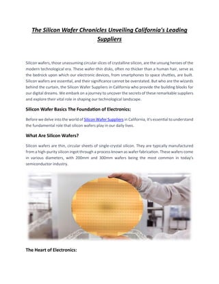
- 1. The Silicon Wafer Chronicles Unveiling California's Leading Suppliers Silicon wafers, those unassuming circular slices of crystalline silicon, are the unsung heroes of the modern technological era. These wafer-thin disks, often no thicker than a human hair, serve as the bedrock upon which our electronic devices, from smartphones to space shuttles, are built. Silicon wafers are essential, and their significance cannot be overstated. But who are the wizards behind the curtain, the Silicon Wafer Suppliers in California who provide the building blocks for our digital dreams. We embark on a journey to uncover the secrets of these remarkable suppliers and explore their vital role in shaping our technological landscape. Silicon Wafer Basics The Foundation of Electronics: Before we delve into the world of Silicon Wafer Suppliers in California, it's essential to understand the fundamental role that silicon wafers play in our daily lives. What Are Silicon Wafers? Silicon wafers are thin, circular sheets of single-crystal silicon. They are typically manufactured from a high-purity silicon ingot through a process known as wafer fabrication. These wafers come in various diameters, with 200mm and 300mm wafers being the most common in today's semiconductor industry. The Heart of Electronics:
- 2. Silicon wafers are the heart of most electronic devices. They serve as the substrate upon which microchips, transistors, and other electronic components are fabricated. These wafers are carefully engineered to have a perfect crystalline structure, making them highly efficient in conducting electricity. This property is what enables the creation of intricate electronic circuits on their surfaces. Silicon Wafers and Moore's Law: Silicon wafers have played a pivotal role in driving the relentless pace of technological advancement. Gordon Moore, co-founder of Intel, famously predicted that the number of transistors on a microchip would double approximately every two years. This prediction, known as Moore's Law, has held true for decades, thanks in no small part to the consistent improvement in silicon wafer manufacturing techniques. California's Silicon Valley A Hub of Innovation: • The Birthplace of Tech Giants California's Silicon Valley, often simply referred to as "Silicon Valley," is synonymous with innovation and technological prowess. Home to giants like Apple, Google, and Tesla, this region has been at the forefront of the global tech industry for decades. It's no surprise, then, that California is also a hotbed for silicon wafer manufacturing. • Silicon Wafer Suppliers in California In California, several companies stand out as leading Silicon Wafer Suppliers, contributing significantly to the state's reputation as a technological powerhouse. • Applied Materials, Inc. Applied Materials, Inc., headquartered in Santa Clara, California, is a global leader in materials engineering solutions. While the company is known for its innovations in semiconductor manufacturing equipment, it also plays a pivotal role in the production of silicon wafers. Applied Materials provides a range of advanced materials, equipment, and services to semiconductor manufacturers worldwide. They are dedicated to enhancing the efficiency and performance of semiconductor devices, including the silicon wafers that underpin them. • Siltronic AG
- 3. Siltronic AG is another key player in California's silicon wafer landscape. Although headquartered in Germany, Siltronic operates a major facility in Portland, Oregon, making it a significant contributor to the region's tech ecosystem. Siltronic is renowned for producing high-quality silicon wafers used in various applications, from consumer electronics to automotive systems. Their commitment to precision and innovation has earned them a prominent place among Silicon Wafer Suppliers in California and beyond. • MEMC Electronic Materials, Inc. MEMC Electronic Materials, Inc., now known as SunEdison, is a company with deep roots in silicon wafer manufacturing. Founded in California in 1959, this company has been a pioneer in the industry, consistently pushing the boundaries of what silicon wafers can achieve. SunEdison produces wafers tailored to the specific needs of various semiconductor applications. They have a strong presence in California, making them an integral part of the state's semiconductor supply chain. The Art and Science of Silicon Wafer Production: Silicon wafer production is a highly complex and precise process. It involves several stages, each of which contributes to the final quality and characteristics of the wafer. Let's take a closer look at the key steps in the manufacturing process: • Ingot Growth The journey of a silicon wafer begins with the growth of a silicon ingot. This ingot is essentially a large, cylindrical crystal of silicon that serves as the raw material for the wafers. The ingot is grown from high-purity silicon, with controlled crystalline orientation to ensure uniformity. • Wafer Slicing Once the silicon ingot has reached the desired size, it's sliced into thin wafers using a precision saw. These wafers are incredibly thin, often measuring just a few hundred micrometers in thickness. • Surface Preparation The surfaces of the wafers are polished to achieve a mirror-like finish. This step is crucial for creating the smooth, defect-free surface required for semiconductor fabrication. • Doping
- 4. To control the electrical properties of the silicon wafers, controlled amounts of specific elements are introduced through a process called doping. This alters the conductivity of the silicon and allows for the creation of transistors and other electronic components. • Photolithography Photolithography is a crucial step in semiconductor manufacturing, where intricate patterns are created on the silicon wafer's surface using masks and light exposure. This defines the layout of transistors, interconnections, and other components on the wafer. • Etching and Deposition Chemical etching and deposition processes are used to remove or add materials to the wafer's surface selectively. This step helps in shaping the various layers of the semiconductor device. • Quality Control Throughout the manufacturing process, rigorous quality control measures are implemented to ensure that each wafer meets the required specifications. Defective wafers are discarded to maintain the highest standards of quality. The Future of Silicon Wafers Challenges and Innovations: While silicon wafers have come a long way in enabling technological progress, there are several challenges that Silicon Wafer Suppliers in California and worldwide must address to sustain this momentum. • Increasing Wafer Size One of the strategies to improve the performance and efficiency of semiconductor devices is to increase the size of silicon wafers. While 300mm wafers are currently the standard, there is ongoing research into the feasibility of producing even larger wafers. However, this poses significant manufacturing and handling challenges. • Reducing Defects As electronic devices become more complex, the tolerances for defects on silicon wafers become increasingly stringent. Suppliers must continually invest in research and development to reduce defects and ensure the highest possible yield of usable wafers. • Environmental Concerns
- 5. The manufacturing of silicon wafers involves several chemicals and energy-intensive processes, raising environmental concerns. Suppliers are under pressure to develop more sustainable production methods and reduce their carbon footprint. Innovations in Silicon Wafer Technology: Despite these challenges, Silicon Wafer Suppliers in California are actively engaged in research and innovation to address these issues and drive the industry forward. • Advanced Materials The development of advanced materials is crucial to improving the performance of silicon wafers. Suppliers are exploring new materials and processes to enhance the thermal and electrical properties of wafers. • 3D Integration Three-dimensional (3D) integration is a promising approach to pack more functionality into a smaller space. Suppliers are working on developing 3D integration techniques that involve stacking multiple layers of silicon wafers, enabling the creation of more powerful and compact devices. • Sustainable Manufacturing In response to environmental concerns, Silicon Wafer Suppliers are investing in sustainable manufacturing practices. This includes recycling and reusing materials, reducing energy consumption, and minimizing waste. Conclusion: In a world driven by technology, Silicon Wafer and Suppliers in California are the silent architects of our digital future. These companies, often operating behind the scenes, provide the foundation upon which our most advanced devices and innovations are built. As we continue to push the boundaries of what's possible in the world of electronics, Silicon Wafer Suppliers remain at the forefront of innovation, constantly striving to meet the challenges of tomorrow while delivering the silicon wafers that power our world today.