
Recommended
More Related Content
Similar to Analog and Digital Conversion Guide: ADCs, DACs, and Signal Types
Similar to Analog and Digital Conversion Guide: ADCs, DACs, and Signal Types (20)
Recently uploaded
Recently uploaded (20)
Analog and Digital Conversion Guide: ADCs, DACs, and Signal Types
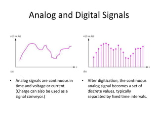
- 1. Analog and Digital Signals • Analog signals are continuous in time and voltage or current. (Charge can also be used as a signal conveyor.) • After digitization, the continuous analog signal becomes a set of discrete values, typically separated by fixed time intervals.
- 2. Digital-to-Analog (D/A) Conversion • For an n-bit D/A converter, the output voltage is expressed as: • The smallest possible voltage change is known as the least significant bit or LSB. VLSB 2n VFS VO (b121 b2 22 ...bn 2n )VFS
- 3. DAC TI’s 20-bit sigma delta DAC
- 4. Analog-to-Digital (A/D) Conversion • Analog input voltage vx is converted to the nearest n-bit number. • For a four bit converter, 0 -> vx input yields a 0000 -> 1111 digital output. • Output is approximation of input due to the limited resolution of the n-bit output. Error is expressed as: V vx (b121 b2 22 ... bn 2n )VFS
- 5. ADC Die Photo • Rockwell Scientific 4Gsps ADC
- 6. A/D Converter Transfer Characteristic V vx (b121 b2 22 ... bn 2n )VFS
- 7. How do ADCs and DACs work? • Many different types! • DAC – DAC #1: Voltage Divider – DAC #2: R/2R Ladder • ADC – ADC #1: Flash – ADC #2: Single-Slope Integration – ADC #3: Successive Approximate (SAR) 7
- 8. DAC #1: Voltage Divider 8 2-to-4 decoder 2 Din Vout Vref R R R R • Fast • Size (transistors, switches)? • Accuracy? • Monotonicity?
- 9. 9 Figure 9.39 An N-bit D/A converter using a binary-weighted resistive ladder network. D/A Converter Circuits • Binary-weighted registers 1 2... N b b b REF REF REF 1 2 1 ... 2 2 O N N V V V i b b b R R R O O f v i R
- 10. DAC #2: R/2R Ladder 10 • Size? • Accuracy? • Monotonicity? (Consider 0111 -> 1000) D3 (MSB) D2 D1 D0 (LSB) 2R 2R 2R 2R R R R 2R Iout Vref
- 11. DAC output signal conditioning 11 • Often use a low-pass filter • May need a unity gain op amp for drive strength
- 12. ADC #1: Flash Converter 12 Vref R R R R Vin + _ priority encoder 3 2 1 0 Vcc 2 Dout + _ + _
- 13. ADC #1: Flash Converter Example 13 Vref R R R R Vin + _ priority encoder 3 2 1 0 Vcc 2 Dout + _ + _ 4 V 3 V 2 V 1 V = 2.5 V ‘H’ ‘H’ ‘L’ ‘H’ 1 2 3 • Resistors divide Vref, e.g. • Let Vref = 4 V • 4 equal resistors => 1 V steps • The 1V, 2V, and 3V signals are fed into the negative input of three comparators • A comparator outputs a logic high (‘H’) if its positive input is greater than its negative input • For comparator #1 and #2, this is indeed the case (2.5 V > 1 V and 2.5 V > 2 V, respectively), so they outputs a logic high, ‘H’ • For comp #3, (2.5 V < 3.0 V), so it outputs a logic low, ‘L’ • A priority encoder outputs the largest numbered input that is high (true). Since 0, 1, and 2 are all true, Dout = 0b10. 0 V 0b10 2.5 2.5 2.5 1.0 2.0 3.0
- 14. ADC #2: Single-Slope Integration 14 + _ Vin n-bit counter CLK EN* Vcc done C I • Start: Reset counter, discharge C. • Charge C at fixed current I until Vc > Vin . How should C, I, n, and CLK (fCLK) be related? • Final counter value is Dout. • Conversion may take several milliseconds. • Good differential linearity. • Absolute linearity depends on precision of C, I, and clock.
- 15. ADC #3: Successive Approximation (SAR) 15 1 Sample Multiple cycles • Requires N-cycles per sample where N is # of bits • Goes from MSB to LSB • Not good for high-speed ADCs