SlideShare a Scribd company logo
1 of 55
What is a Microprocessor?
• The word comes from the combination Micro
(indicating very small size) and Processor
(process means to manipulate e. g. certain
operations on the numbers).
• Definition of the Microprocessor
A programmable device that takes in
numbers, performs on them arithmetic or
logical operations according to the program
stored in memory and then produces other
numbers as a result
Difference between:
– Microcomputer – a computer with a microprocessor as its CPU.
Includes memory, I/O etc.
– Microprocessor – A silicon chip which includes ALU, registers
(as a small internal memory) & a control unit.
A general purpose device (i.e. may be used for different
purposes in different applications e.g. as a CPU in a
microcomputer)
 Uses Memory, I/O functions etc external to the chip
 Configuration of the system is flexible
– Microcontroller - A silicon chip which includes microprocessor,
memory & I/O etc & other peripheral functions all integrated
on a single chip.
 More application specific, single purpose
Especially used in embedded systems
 Fixed configuration (i.e. fixed memory & other functions)
Memory
OutputInput
A Microprocessor-based system
A microprocessor based system (e.g. a microcomputer)
consists of the following components:
• Internally, the microprocessor is made up of
3 main units.
– The Arithmetic/Logic Unit (ALU)
– The Control Unit.
– An array of Registers as a small internal
memory for holding data while it is being
manipulated or processed.
ALU
Register
Array
Control
Inside a Microprocessor
Memory of Microprocessor
• Inside (very small)
– The registers inside the microprocessor
• Outside
– Read Only Memory (ROM)
• used to store information that does not change
– Random Access Memory (RAM)
• used to store information supplied by the
user such as programs and data.
8085 Microprocessor
• One of the most popular 8-bit general purpose µp
launched by Intel, USA in 1976
• An N-MOS chip with 40 pins & +5V supply
• Capable of addressing 216 = 64 KB of memory
• It works on 3 MHz clock.
• It has multiplexed address and data bus (AD0-AD7)
to reduce hardware (no. of pins) on the chip
• It has 74 basic instructions (formats) with 5 different
addressing modes.
Frequency
Generator is
connected to
these pins
Power
Supply: +5 V
Address latch Enable
(to activate latch to
store address
Read
Write
Input/Output/
Memory
Multiplexed
Address/Data
Bus
(Bidirectional)
Address Bus
(Unidirectional)
To connect
slow peripherals
Interrupts
For DMA
Request
For Serial data
communication
Similar function pins are
grouped in this figure- (called
functional pin diagram)
 AD0-AD7: Lower order bidirectional multiplexed Address/Data lines.
 A8-A15: Higher order unidirectional address lines, carries only address
 ALE: A pulse output signal from this pin is used by microprocessor to
enable an 8-bit external latch to save the lower order address bits
 S0,S1: These output status signals are used to indicate type of operation
 RD: MP reads data from memory/IO device when this pin is active (low)
 WR: MP writes data into memory/IO device when this pin is active (low)
 READY: This pin is used by slow-responding peripheral devices to
indicate the µP whether they are READY to send/accept data to/from µP
 TRAP: A highest priority , non mask able vectored interrupt. After TRAP,
restart occurs and execution starts from predefined vector address 0024H
 RST5.5,6.5,7.5:These are maskable, vectored interrupts and have lower
priority than TRAP
 INTR: INTR is a lowest priority non-vectored which can be used to
connect upto 8 peripheral devices by using an interrupt controller
 INTA: An interrupt acknowledge signal pin for INTR, only
acknowledgment pin among all interrupts
PIN FUNCTIONS
 HOLD & HLDA: When a peripheral device wants to gain control of system
buses (e.g. for a DMA operation), it sends request to µP via this input pin.
In response, µP activates HLDA (output) to acknowledge the request &
temporarily releases control over system buses.
 IO/M: This output control pin is used to indicate whether the read/write
operation being performed by microprocessor is for memory (when low)
or for I/O device (when high)
 RESET IN: This control input signal connected to external RESET button to
bring µP in initial standby mode. It restarts µp to memory location 0000H.
 RESET OUT: When high, this indicates µP has been reset
 SID & SOD: These pins are used for serial data communication by using
making use of SIM & RIM instructions
 X1X2 :These are clock input signals which are connected to external
oscillator of 6 MHz frequency which is divided by 2 internally in 8085 to
generate 3 MHz operating frequency .
 CLK (out): Used to provide same 3MHz clock to the rest of the system
 VCC, VSS & GND: Power supply pins VCC= +5V & VSS=GND=0V
PIN FUNCTIONS
Architecture of 8085 Microprocessor
Functions of various building blocks:
ALU: Arithmetic & Logic Unit contains digital circuitry to perform all
arithmetic & logical operations in 8085
TIMING & CONTROL UNIT: Generates various types of control signals to
direct microprocessor what & when a task is to be performed.
INSTRUCTION DECODING & MACHINE CYCLE ENCODING: Used to
decode instruction opcode into binary form & to control various machine
cycle operations during execution of an instruction
SERIAL I/O CONTROL: Used to control serial data communication with
external devices via SID/SOD lines
INTERRUPT CONTROL: Used to handle various incoming interrupts which
occur via 5 interrupt pins TRAP, RST7.5, RST6.5, RST5.5 & INTR lines
INCREMENTER/DECREMENTER ADDRESS LATCH: It increments/
decrements contents of Program Counter or Stack Pointer when
instructions related to them are executed.
ADDRESS & DATA BUFFERS: These are used to momentarily hold the 16
‘in-transit’ address bits while they are being placed on Address/Data bus.
These effectively act as an ‘interface’ between internal & external buses.
GENERAL PURPOSE REGISTERS (B,C,D,E,H,L): These 6 register can be used
singly to store any 8-bit data or as register pairs (valid pairs are B-C, D-E &
H-L) to perform 16-bits operations.
TEMPORAY REGISTERS (W, Z & TR): Used internally by 8085 to temporarily
store 8-bit data (or partial results) while performing various arithmetic
operations. Not available to user
ACCUMULATOR: An 8 bit register having some special features (usually
included in ALU block). It stores results of arithmetic & logical operations.
Many instructions in 8085 are Accumulator-based.
INSTRUCTION REGISTER: An 8-bit register used to hold opcode of the
instruction currently being executing
PROGRAM COUNTER: Holds 16-bits address of the next byte to fetched
during execution of an instruction & is incremented by 1 each time a byte is
fetched to point to the next memory location.
STACK POINTER: A 16-bits register which holds the address of topmost
memory location of stack. It decrements/increments by 2 each time a
PUSH/POP operation is performed
FLAG REGISTER: An 8 bit register whose individual bit are set/reset
according to status of result generated by ALU.
S Z X AC X P X CY
S: Sign flag is set when result of an operation is negative (leftmost
bit is 1 in signed arithmetic operations)
Z: Zero flag is set when result of an operation is zero otherwise reset
AC: Auxiliary carry flag is set when there is a carry out of 3rd to 4th
bit in an 8-bit operation
CY: Carry flag is set when there is a final carry generated in an
operation.
P: Parity flag is set when result contains even number of 1’s (Reset
for odd number of 1’s )
Program Status Word: The combined 16-bits contents of
Accumulator & Flag register (A & F) are named as PSW
FLAG REGISTER
Set = 1, Reset = 0
Accumulator (8-bits) Flag Register (8-bits)
PSW (16 bits)
Procedural steps of an example instruction (MOV C, A) (Hexcode: 4F) being fetched &
executed by microprocessor from memory location 2005:
Step 1: 8085 places 16-bits address (2005H) from program counter on address bus
Step 2: Control unit activates RD signal to enable memory chip (RAM)
Step 3: Instruction byte (4F) is placed by memory on data bus
Step 4: Instruction is decoded by Instruction decoder in binary form which directs timing
& control unit to generate appropriate control signals to carry out the task as specified by
the instruction
INSTRUCTION FETCH & EXECUTION OPERATION IN 8085
• AD7-AD0 lines serve dual purpose; they work in time-
shared mode: at one time they carry address & data
at other time, to save 8 extra pins on the chip
• For a read/write operation from memory, we must
provide complete 16-bit address for full duration (3
clock periods) of read/write cycle (until data is loaded
to/from memory.
• The 8 higher-order bits of the address remain on the
bus for full read/write cycle, but low-order bits
remain for only 1 clock period (to make data bus free
to carry data later). So we use an external 8-bit latch
(a chip) to save & hold lower-order address for the
remaining time (2 clock periods) or else it (lower
order address) would be lost.
• We use ALE control signal to activate (to save lower
order address) latch in the first clock period.
Multiplexing/Demultiplexing AD7-AD0
A15-A8
LatchAD7-AD0
D7- D0
A -A7 0
8085
ALE
WR RD IO/M
CS
Memory
Chip
RD WR
A9-A0
A15-A10
Chip Selection
Circuit
Multiplexing/Demultiplexing AD7-AD0
Activated for a
read (IN)
operation
Activated for a
write (OUT)
operation
Activated in the
first clock cycle (T1)
to save lower order
address in latch Latch provides address to
memory for remaining time
IN OR OUT
The 8085 Instructions (Summary)
The 8085 instructions can be categorized
into 5 different groups:
• Data Transfer
• Arithmetic
• Logic
• Branch
• Machine Control
DATA TRANSFER GROUP
MOV Rd, Rs : Copy Rs to Rd
MOV R/M, M/R: Copy contents of M (addressed by HL) to R or vice versa
MVI R, data (8): Move 8-bit immediate data to R
MVI M, data (8): Move 8-bit immediate data to M
LXI Rp, data (16): Move 16-bit immediate data to Rp
LDA addr: Copy contents of given memory address to A
STA addr: Copy contents of A to given memory address
LHLD addr: Copy contents of given+next address to L,H respectively
SHLD addr: Copy contents of L,H to given+next address respectively
LDAX Rp : Copy contents of location addressed by Rp to A
STAX Rp: Copy contents of A to location addressed by Rp
XCHG: Exchange contents of HL & DE
ARITHEMATIC GROUP
ADD/SUB R: A+R/A-R, result in A
ADD/SUB M: A+M/A-M, result in A, M addressed by HL
ADC/SBB R: A+R+CY/A-R-CY, result in A
ADC/SBB M: A+M+CY/A-M-CY, result in A
ADI/SUI, data (8): A+data/A-data, result in A
ACI/SBI, data (8): A+data+CY/A-data-CY, result in A
DAD rp: HL+Rp, result in HL
INR/DCR R: R+1/R-1
INR/DCR M: M+1/M-1, M addressed by HL
INX/DCX Rp: Rp+1/Rp-1
DAA: Produces result in BCD (or decimal) form, instead
of usual hexadecimal. Can be used immediately after any
of the addition type instruction in any program for this
purpose, but not usable after any subtraction instruction
LOGICAL GROUP
ANA/ ORA / XRA R: AND/OR/EX-OR A with R, result in A
ANA/ORA/XRA M: AND/OR/EX-OR A with M, result in A
ANI/ORI/XRI, data (8): AND/OR/EX-OR A with data, result in A
CMP R: A-R, only flags changed as per result, then result discarded
CMP M: A-M, only flags changed as per result, then result discarded
CPI, data (8): A-data,only flags changed as per result, then result discarded
STC: Set (change to 1 if not already) the carry (CY) flag
CMC: Complement (0 to 1 or vice versa) the carry (CY) flag
CMA: Complement (0 to 1 or vice versa) the Accumulator
RAL/RAR: Rotate Accumalor left/right by 1 bit through carry (CY) flag
RLC/RRC: Rotate Accumalor left/right by 1 bit, also copy 7th bit of A to CY
BRANCH CONTROL GROUP
Jump: Program counter is loaded with (jumps to) given address, doesn’t return back
 Unconditional: JMP addr: Jump to given address unconditionally
 Conditional: JZ/JNZ/JC/JNC/JP/JM/JPE/JPO addr: Jump to given address
depending on corresponding flag condition
Call: Program counter jumps to given address, saves address of next instruction in the
stack, returns back (redirected by RET instruction) after execution of a subroutine
which is stored at the given address
 Unconditional: CALL addr: Jump to given address unconditionally, return back
after execution of subroutine
 Conditional: CZ/CNZ/CC/CNC/CP/CM/CPE/CPO addr: Jump to given address
depending on corresponding flag condition, returns back after execution of subroutine
Return: Program counter is loaded with return address that was saved in the stack at
the start of CALL instruction . Last instruction of a subroutine is always a return
instruction to redirect the microprocessor back to the main program
 Unconditional: RET: Retrieves saved return address from the stack back to the PC
 Conditional: RZ/RNZ/RC/RNC/RP/RM/RPE/RPO: Retrieves saved return address
from stack back to the PC depending on the corresponding flag condition
RSTn (Total 8 instructions from RST0 to RST7 for n= 0 to 7): An unconditional
CALL instruction but with predefined address (8 different addresses for n=0 to 7)
I/O, STACK & MACHINE CONTOL GROUP
IN port-addr (8): Copy 8-bit data available at 8-bit input port address to A
OUT port-addr (8): Copy contents of A to given 8-bit output port address
PUSH Rp: Store contents of given Rp in top two locations of stack
POP Rp: Load Rp with contents of top two locations from stack
PUSH PSW: Store 16-bit contents of PSW (contents of A & flag register) into
top two locations of stack
POP PSW: Load 16-bit contents of top two locations of stack into PSW (A &
flag register)
XTHL: Exchange contents of HL with top two locations of stack
SPHL: Copy contents of HL to stack pointer
EI/DI: Enables/Disables all maskable interrupts
SIM/RIM: Explained earlier
NOP: No operation performed, used to provide delay in some programs
HLT: Halts the program
INSTRUCTION WORD SIZE IN 8085
• One-Byte Instructions: Occupies 1 byte in the
memory, no 8/16 bits data is included in the instructions
Examples: MOV A, B ADD B RAL MOV C, M
CMC STC CMP M ANA B INR C
• Two-Bytes Instructions: Occupies total 2 bytes in the
memory, 8-bits data is included in the instructions
Examples: MVI A, 05 IN 02 CPI 03
• Three-Bytes Instructions: Occupies total 3 bytes in
the memory, 16-bits data is included in the instructions
Examples: LXI H, 2500 LDA 3050 LHLD 2600
8085 ADDRESSING MODES
Addressing Mode: An addressing mode indicates the location
of operand in an instruction
1. IMMEDIATE: Operand itself is immediately given in the instruction
Examples: MVI A,05H LXI H, 2050H ADI 02
2. DIRECT: 16 bits address (or 8 bit in case of I/O instructions) is
directly given in the instruction itself
Examples: LDA 2500H IN 06 SHLD 2605 OUT 03
3. REGISTER: Operand is given in one of the registers
Examples: MOV B,C DCR C SUB D ANA H ADD B
4. REGISTER INDIRECT: 16-bits address of operand is indirectly
provided in one of the register pairs
Examples: MOV A, M ADD M INR M LDAX B STAX D
5. IMPLICIT (or IMPLIED): Operand is in the Accumulator
Examples: RAL CMA RRC RLC
MACHINE CYCLES & TIMING DIAGRAMS
Instruction Cycle: Total time required to execute an instruction.
Includes opcode fetch & execution cycles
Machine Cycle: Time required by µP to complete one operation
(read/write/fetch) of accessing memory or I/O devices during execution
of an instruction. Machine cycles are of fetch, memory read/write & I/O
read/write type. First machine cycle is always an opcode fetch cycle in
an instruction cycle. An instruction in 8085 may have minimum 1
(which is a fetch cycle) to a maximum of 5 machine cycles depending
on type of instruction.
T-State: A subdivision of an operation (read/write/fetch) carried out in
one system clock period. In 8085, while a fetch cycle in all instructions
requires 4 T-states, other machine cycles may require minimum 3 to a
maximum of 6 T-states depending upon type of instruction.
Timing Diagram: A timing diagram is a graphical representation of
various control signals generated during execution of an instruction. It
depicts status of important control signals in each T-state of all machine
cycles involved in the execution of an instruction.
Machine cycle 2 Machine cycle 5
Instruction cycle
Machine cycle1
T – State 1
T – State 2
T – State 3
T – State 6
Execution Cycle
(MR/MW/IOR/IOW)
Opcode
Fetch Cycle
1 T-State= 1 Clock cycle
INSTRUCTION CYCLE, MACHINE CYCLE, FETCH CYCLE, EXECUTION CYCLE
4 T-states
No. of m/c
cycles reqd.
1
2
3
4
5
CALCULATION OF MACHINE CYCLES
Example Instructions
MOV A, B HLT STC CMA XCHG INR C NOP SIM
MVI A, 05 MOV B, M LDAX B ADD M RET
LXIH, 2000 MVI M, 79H JMP 3050 IN 01 RSTn
LDA 2500 STA 3501
CALL 2601 LHLD 2300 XTHL SHLD 3600
ALE
RD
WR
IO/M
T1 T2 T3 T4
Some Instructions require
only 1 machine cycle
which is an opcode fetch
cycle
For Example:
MOVA, B
stored at 2000H in any program
Opcode (or Hex code) is:
78H
Note: A fetch cycle always
requires 4 T-states
CLK
A15-A8
TIMING DIAGRAM: OPCODE FETCH CYCLE
AD0-AD7
20H
78H00H
INOUT
S0 & S1 control signals may also be shown in the above & all other timing diagrams. They
may be shown separately or combined with IO/M
01H 45H
25H
00H 3EH
RD
IO/M
Op-Code Fetch Cycle Memory Read Cycle
T1 T2 T3 T4 T5 T6 T7
25
Instruction:
MVIA, 45H
stored at 2500H
location
Hex Codes:
3E, 45H
WR
ALE
A8- A15
Example Timing Diagram of an instruction requiring 2 machine cycles
AD0 -AD7
CLK
 A memory read
cycle is exactly equal
to fetch cycle except it
requires 1 extra T-
state & also S0=0
Example Timing Diagram of an instruction requiring 3 machine cycles
Instruction: LXI H, 2035H stored at 3010H. Hex Codes: 21H, 35H, 20H
T1 T2 T3 T4 T5 T6 T7 T8 T9 T10
21H 11H 35H 12H 20H
30H 30H 30H
ALE
RD
WR
IO/M
10H
Op-Code Fetch Cycle Memory Read Cycle Memory Read Cycle
IN OUT IN OUT INOUT
A8- A15
AD0 -AD7
L Reg Content Of M00H 7EH
ALE
RD
WR
IO/M
Op-Code Fetch Cycle Memory Read Cycle
T1 T2 T3 T4 T5 T6 T7
Content Of Reg H26H
MOVA, M
stored at 2600H
Hex Code: 7E
Another example of an instruction requiring 2 machine cycles
INOUT OUTIN
A8- A15
AD0 -AD7
LReg Content of RegA00H 7EH
ALE
RD
WR
IO/M
Op-Code Fetch Cycle Memory Write Cycle
T1 T2 T3 T4 T5 T6 T7
Content Of Reg HA0H
IN OUTOUTOUT
AD0 -AD7
A8- A15
MOV M, A
stored at 2600H
Hex Code: 77H
Another example of instruction requiring 2 machine cycles
STACK & SUBROUTINES
(ILLUSTRATION OF PUSH/POP AND
CALL/RET INSTRUCTIONS)
THE STACK
What is Stack?
• The stack is a group of memory locations set aside by user in memory area
for temporary storage (i.e. it is a portion of RAM itself) because 8085 has
limited no. of registers. In addition, it has some special features.
• Starting address of stack (initialization of stack) is defined by user by
loading a 16-bit address into Stack Pointer as below:
LXI SP, XXXX
where XXXX is any 16-bits address chosen by user
When is Stack used?
1. Stack is used to save the return address of Program Counter when:
 A CALL/RSTn instruction (a software interrupt) encounters in a program
 A hardware interrupt occurs during execution of a program
In any of the above cases:
i) µP executes the current instruction at hand & saves address of the next
instruction (i.e. contents of PC, the return address) in stack so that it knows
where it was before jumping to the subroutine/ISR of the respective interrupt.
ii) Microprocessor loads PC with starting address of subroutine (in case of a
CALL instruction) or ISR (in case of a hardware interrupt)
iii) Microprocessor executes respective subroutine/ISR
iv) Microprocessor retrieves back the saved return address from the stack (by
using RET instruction, which is the last instruction of all subroutines) and
loads back it into PC.
v) Microprocessor re-continues the main program as usual
 In the above cases, use of stack is made by µP internally. User only
defines its starting address
2. Stack can also be used by user ‘manually’ to temporarily store the contents
of a register pair (& not a single register) so that it be used for other
operations or purposes. For example, consider HL pair has some specific
address or data stored in it at the start of a program. Now a user wants to
‘free’ the HL pair for using in some other instructions in the program but at
the same time doesn’t want to lose the initial contents. For this, he can save
contents of HL pair in stack, use HL pair in other instructions & then get
back saved contents from stack. Storage (called PUSHing) & retrieval (called
POPing) of any contents to/from stack is achieved by using PUSH & POP
instructions respectively.
STACK PRINCIPLES
• The storage and retrieval of any content on the stack follows the Last-In-
First-Out (LIFO) sequence.
• The stack normally grows backwards into memory
• Stack Pointer is a 16-bits register located in 8085 chip, which holds the
address of topmost location (called Stacktop) of stack. The contents of SP are
decremented/incremented by 1 with storage/retrieval of a each byte into stack
• Although stack can be initialized anywhere in the memory area, usually it is
initialized at the highest available memory location so that chances of
interference between stack locations & user program are minimized because
address in Stack Pointer is decremented with each byte storage into stack i.e.
stack will grow backwards into memory (towards user program)
• The first location available for a write (or PUSH) operation in stack is one
that is addressed by SP-1 & not the SP. However, the first location for a read
(or POP) operation is one that is addressed by SP. During PUSHing, the
stack operates in a “Decrement then Store” style i.e. decrement SP first then
store at the new (lower) location address as indicated by SP. During POPing,
the stack operates in a “Use then Increment” style i.e. read the contents of
topmost location (addressed by SP) first & then increment it to indicate
towards a new (higher) topmost location.
EXAMPLE OF PUSH/POP INSTRUCTIONS
Consider the following program:
2000 LXI SP, 2099H
2003 LXI H, 42F2H
2006 PUSH H
…
…
…
2010 POP D
…
…
Load SP with an arbitrary address, say 2099, to initialize stack
Load any 16 bit value in the HL register pair, say 42F2
The content of the HL register pair are pushed (written) into stack.
Contents of H (42H) are stored first in the location addressed by SP-
1* i.e. 2098 (higher location for higher register) & contents of L
(F2H) are stored then in SP-2 i.e. 2097 (lower location for lower
register). New address in SP after the PUSH operation is 2097.
Contents of two locations from stack are loaded into DE pair. The
1st location is addressed by SP** (now containing 2097) & the 2nd
location is addressed by SP+1 (2098). So, E is loaded first with F2H
& then D is loaded with 42H. New address in SP after this POP
operation is 2098.
Note: *As mentioned earlier, the first available location for storage in the stack is always SP-
1 (2098 in the above example). Also, because a PUSH instruction copies contents of a
register pair (HL, BC or DE), it requires two (consecutive) memory locations in the stack.
** As mentioned earlier, the first memory location that is readable from stack is SP (=2097
here, after execution of PUSH instruction). Also, because a POP instruction loads a register
pair, it reads two locations (bytes) from the stack
 The SP is decremented by one to
2098H, & the contents of the H
register (42H) are copied to
memory location 2098H
 The SP is again decremented by
one to 2097H & the contents of
the L register (F2H) are copied to
memory location 2097H
 New SP contents after PUSH
operation are 2097
Execution of PUSH H
42 F2
Flag
C
E
L
A
B
D
H
SP
F2
42
X
2097
2098
2099
2097
8085 Registers
Stack
Execution of PUSH H instruction, as explained in the previous
example, is illustrated here:
Contents of SP & stack locations
after PUSH H operation
 The contents (F2H) of the current
stacktop location (2097H) are copied
to E register and the SP is
incremented by one to 2098H
 The contents of the new top
location (2098H) of the stack
are copied to D register, and the
SP is incremented by one again
 Address of new topmost location
(contents of SP) now becomes
2099H after the POP operation
42 F2
2099
F
C
E
L
A
B
D
H
SP
8085 Register
Execution of POP D
Contents of SP & stack locations
after POP D operation
Execution of POP D instruction, as explained in the previous
example, is illustrated here:
F2 2097
42 2098
X 2099
Stack
PUSH PSW instruction is similar to PUSH Rp instruction except that it stores PSW
(the 16-bits combined contents of Accumulator & Flag Register) instead of a general
purpose register pair into the stack
12 80
80
12
X
FFFB
FFFC
FFFE
FFFF
PUSH PSW
Stack
A (8) Flag(8)
For example assume Accumulator & Flag
registers contain 12H & 80H respectively.
Assume stack is initialized at FFFFH (i.e.
contents of SP) then on execution of
PUSH PSW:
 SP is decremented by one & the
contents of Accumulator (12H) are
copied first to the FFFEH location
 SP is decremented by one again & the
contents of Flag register (80H) are
copied then to the FFFDH location
 New contents of SP are FFFDH after
the PUSH PSW operation. Contents of SP & PSW
after PUSH PSW operation
FFFDSP
POP PSW instruction is similar to POP Rp instruction except that it reads contents
of top two locations from the stack & loads them into PSW (or Accumulator & Flag
Register)
12 80
80
12
X
FFFB
FFFC
FFFD
FFFE
POP PSW
Stack
A FContinuing with example of PUSH PSW
explained earlier, we assume that
current address in SP is FFFDH having
value 80H. Then, on execution of POP
PSW following actions take place in
steps:
 Contents of top location addressed by
SP (i.e. 80H) are copied to the Flag
register first.
 SP is incremented by one & the
contents of current top location (now
FFFEH) are copied to the Accumulator.
 SP is incremented by one again & the
contents of current top location now
become FFFFH.
SP FFFF
Contents of SP & PSW
after POP PSW operation
 A subroutine is group of instructions (a subprogram) written separately from
the main program to perform a function that occurs repeatedly in the main
program
 When a main program CALLs a subroutine, the program execution is
transferred to the subroutine. After the completion of the subroutine ,the
program execution returns to the main program.
 The microprocessor uses stack to store the return address.
 8085 has two instructions for dealing with subroutines:
– The CALL instruction, used to redirect program execution to the
subroutine. Format of CALL instruction is:
CALL XXXX (where XXXX is 16-bits starting address of the subroutine)
A CALL instruction may be of conditional or unconditional type
– The RET instruction, used to return to the main program at the end of
the subroutine. No address is provided by user in a return instruction as
it automatically retrieves return address from the stack top locations.
RET may also be of conditional or unconditional type
 A CALL instruction is always used in conjunction with RET instruction
SUBROUTINE
EXECUTION OF CALL/RET INSTRUCTIONS
Following sequence of actions take place in when
microprocessor encounters a CALL instruction in the middle of
a program (same steps are taken by microprocessor when a
hardware interrupt occurs in the middle of program):
 Microprocessor saves the address of next instruction (i.e.
contents of PC, the return address) in the stack so that it
knows where it was before jumping to the subroutine.
 Microprocessor loads PC with 16-bits starting address
(provided in the instruction ) of the subroutine
 Microprocessor executes the subroutine
 Microprocessor retrieves back the saved return address from
the stack (by using RET instruction, the last instruction of
subroutine) and loads back it into the PC
Microprocessor re-continues the main program as usual
2000 ….
2001…
2002 …
2003 CALL 3000
2006 …
2007 …
2008 ...
2009 CALL 3000
200C …
200D …
… …
3000 .…
3001 ….
3002 ….
…. ….
RET
Consider the following situation in which microprocessor is executing a (main)
program (stored at 2000H onwards in RAM) & faces CALL instructions at 2003H &
2009H locations. Assuming subroutine is stored 3000H onwards, microprocessor
saves address of next instructions (2006H & 200CH respectively) in the stack, loads
starting address (3000H) of subroutine into PC & executes the subroutine. At the end
of the subroutine, RET instruction instructs microprocessor to retrieve the saved
return addresses which are then loaded back into PC & thus microprocessor continues
the main program as before.
Main Program
Subroutine
8085 INTERRUPTS
• An interrupt is a hardware or software initiated subroutine CALL.
• An interrupt is considered to be an emergency signal that is serviced
by the Microprocessor as soon as possible.
• What happens when MP is interrupted ?
When microprocessor receives an interrupt signal, it suspends the currently
executing program and jumps to a new memory location (interrupt vector) to
execute an Interrupt Service Routine (ISR) in response to the incoming
interrupt. There are two ways of redirecting the execution to the ISR
depending on whether the interrupt is vectored or non-vectored.
Vectored: The address of the subroutine is already known to the
microprocessor
Non Vectored: The external device supplies the address of the subroutine to
the Microprocessor
 Interrupts are also categorized as SOFTWARE & HARDWARE interrupts. In
8085:
SOFTWARE Interrupts: RST n & CALL instructions
HARDWARE Interrupts: TRAP, RST 7.5, 6.5, 5.5, INTR
 An interrupt vector is a pointer or memory address where the ISR is stored
in the memory
 All interrupts are mapped onto a particular memory area called the Interrupt
Vector Table (IVT) which shows vector addresses for each interrupt
 For each type of interrupt, a unique ISR is written at respective vector
locations which directs microprocessor to take some predefined action (s)
 An RSTn instruction is equivalent to a CALL instruction but with a fixed
address & occupies only a 1byte as compared to 3bytes by a CALL instruction
Pin or interrupt Predefined Vector
addresses for 8085
hardware interrupts
TRAP 0024
RST 5.5 002C
RST 6.5 0034
RST 7.5 003C
INTR *
* the address of the ISR is determined by the
external hardware (or interrupt controller)
RSTn
Instruction
Equivalent to
RST0 CALL 0000H
RST1 CALL 0008H
RST2 CALL 0010H
RST3 CALL 0018H
RST4 CALL 0020H
RST5 CALL 0028H
RST6 CALL 0030H
RST7 CALL 0038H
INTERRUT
VECTOR
TABLE
SHOWING
ADDRESS
MAPPING OF
ALL
VECTORED
INTERRUPTS
OF 8085
Execution of an Interrupt
Upon receiving an Interrupt signal, microprocessor saves the
memory location of the next instruction on the stack and the
program is transferred to a new memory location specified by
its vector address where microprocessor executes an ISR. All
other maskable interrupts are automatically disabled until
current interrupt is attended
 An ISR is a predefined set of instructions (a subprogram)
which performs a specific task. It must include the EI
instruction in one of the ending instructions so that all
interrupts are re-enabled for coming in future
 Last instruction of an ISR must always be an RET
instruction which instructs microprocessor to retrieve the
saved return address from the stack so that program is
transferred back to where the program was interrupted.
COMPARISON OF 8085 HARDWARE INTERRUPTS
Interrupt
Name
Priority Maskable
Masking
Method
Vectored
Triggering
Method
INTR Lowest Yes DI / EI No
Level
Sensitive
RST 5.5 /
RST 6.5
Yes
DI / EI
SIM
Yes
Level
Sensitive
RST 7.5 Yes
DI / EI
SIM
Yes
Edge
Sensitive
TRAP Highest No None Yes
Level &
Edge
Sensitive
SIM Instruction
SDO
SDE
XXX
R7.5
MSE
M7.5
M6.5
M5.5
RST5.5 Mask
RST6.5 Mask
RST7.5 Mask
}0 –Available
(not masked)
1 - Masked
Mask Set Enable
0 - Ignore bits 0-2
1 - Set the masks according
to bits 0-2
Force RST7.5 Flip Flop to resetNot Used
Enable Serial Data
0 - Ignore bit 7
1 - Send bit 7 to SOD pin
Serial Data Output
While EI/DI instructions enable/disable all maskable interrupts at once, SIM
instruction can be used to selectively mask (or disable) 3 out of 4 maskable
interrupts which are RST7.5,RST6.5 & RST5.5. Fourth maskable interrupt INTR
can only be enabled/disabled by using EI/DI instructions.
SIM instruction can be used to perform two different tasks: 1. For masking of 3
interrupts 2. For serial data transmission (Each time a SIM instruction is executed, 7th bit
of Accumulator is automatically copied to SOD pin of 8085)
Example of how to use SIM instruction in any program
Example problem:- Set the interrupt masks so that RST5.5 is enabled, RST6.5 is
masked & RST7.5 is enabled.
• We can determine the bit pattern as per format of SIM instruction given
below:
SDO
SDE
XXX
R7.5
MSE
M7.5
M6.5
M5.5
- Enable 5.5
- Disable 6.5
- Enable 7.5
- Allow setting the masks
- Don’t reset the flip flop
- Bit 5 is not used
- Don’t use serial data
- Serial data is ignored
bit 0 = 0
bit 1 = 1
bit 2 = 0
bit 3 = 1
bit 4 = 0
bit 5 = 0
bit 6 = 0
bit 7 = 0
0 0 0 0 1 0 1 0
Contents of accumulator are: 0AH
EI
MVI A, 0A
SIM
• Now use following set of instructions to implement required masks using SIM
 First of all enable all interrupts using EI instruction without using which SIM wouldn't be
effective
 Move the prepared bit pattern (0AH here) to Accumulator
 SIM instruction interprets contents of Accumulator same as per the above format &
performs the desired operation of masking the respective interrupts
RIM instruction
SDI
P7.5
P6.5
P5.5
IE
M7.5
M6.5
M5.5
7 6 5 4 3 2 1 0
RST5.5 Mask
RST6.5 Mask
RST7.5 Mask
}
Indicate current
masking status of
interrupts set by user
(using SIM)
0 -Available
1 - Masked
Status of Interrupt Enable Flip Flop: 1
Set 0 Reset
Serial Data In
RST5.5 Interrupt Pending
RST6.5 Interrupt Pending
RST7.5 Interrupt Pending
Like SIM instruction, RIM can be used to perform two different tasks: 1. To read current
status of 3 maskable interrupts 2. For serial data reception (Each time a SIM instruction
is executed, the bit present on SID pin of 8085 is automatically moved to 7th bit of the
Accumulator)
Pending Interrupts: Since the 8085 has 5 interrupt lines, another interrupts may
occur while an interrupt is being attended and thus remain pending. Such
interrupts are called pending interrupts & would be attended as soon as ISR of
current interrupt is executed. A programmer may know the status (current value of
high/low on the respective interrupt pin) of such interrupts anytime by using RIM
instruction.
An example of Memory Mapping & Address allocations in 8085
The memory map is a pictorial representation of the
memory address ranges of different memory chips (for
example 5 no. of chips here) of different sizes and shows
where they are located within the full address range
available.
0000
AddressRange
EPROM
RAM 1
RAM 2
RAM 3
RAM 4
0000
8FFF
9000
A3FF
A400
Address Range of EPROM Chip
3FFF
4400
Address Range of 1st RAM Chip
5FFF
6000
Address Range of 2nd RAMChip
Address Range of 3rd RAMChip
Address Range of 4th RAMChip
F7FF
FFFF

More Related Content

What's hot

8086-instruction-set-ppt
 8086-instruction-set-ppt 8086-instruction-set-ppt
8086-instruction-set-ppt
jemimajerome
 
8085 interrupts
8085 interrupts8085 interrupts
8085 interrupts
Ram Babu
 

What's hot (20)

TRAFFIC LIGHT CONTROL SYSTEM USING 8085 MICROPROCESSOR
TRAFFIC LIGHT CONTROL SYSTEM USING 8085 MICROPROCESSORTRAFFIC LIGHT CONTROL SYSTEM USING 8085 MICROPROCESSOR
TRAFFIC LIGHT CONTROL SYSTEM USING 8085 MICROPROCESSOR
 
Microprocessor Interfacing and 8155 Features
Microprocessor Interfacing and 8155 FeaturesMicroprocessor Interfacing and 8155 Features
Microprocessor Interfacing and 8155 Features
 
8086-instruction-set-ppt
 8086-instruction-set-ppt 8086-instruction-set-ppt
8086-instruction-set-ppt
 
8085 instruction set
8085 instruction set8085 instruction set
8085 instruction set
 
Architecture of 8085 microprocessor
Architecture of 8085 microprocessorArchitecture of 8085 microprocessor
Architecture of 8085 microprocessor
 
Timing diagram 8085 microprocessor
Timing diagram 8085 microprocessorTiming diagram 8085 microprocessor
Timing diagram 8085 microprocessor
 
Direct memory access (dma) with 8257 DMA Controller
Direct memory access (dma) with 8257 DMA ControllerDirect memory access (dma) with 8257 DMA Controller
Direct memory access (dma) with 8257 DMA Controller
 
8259 Programmable Interrupt Controller
8259 Programmable Interrupt Controller8259 Programmable Interrupt Controller
8259 Programmable Interrupt Controller
 
Interrupts of microprocessor 8085
Interrupts of microprocessor  8085Interrupts of microprocessor  8085
Interrupts of microprocessor 8085
 
8051 Addressing Modes
8051 Addressing Modes8051 Addressing Modes
8051 Addressing Modes
 
Question paper with solution the 8051 microcontroller based embedded systems...
Question paper with solution  the 8051 microcontroller based embedded systems...Question paper with solution  the 8051 microcontroller based embedded systems...
Question paper with solution the 8051 microcontroller based embedded systems...
 
PIC 16F877A by PARTHIBAN. S.
PIC 16F877A   by PARTHIBAN. S.PIC 16F877A   by PARTHIBAN. S.
PIC 16F877A by PARTHIBAN. S.
 
Pic microcontroller architecture
Pic microcontroller architecturePic microcontroller architecture
Pic microcontroller architecture
 
8257 DMA Controller
8257 DMA Controller8257 DMA Controller
8257 DMA Controller
 
8085 interrupts
8085 interrupts8085 interrupts
8085 interrupts
 
System bus timing 8086
System bus timing 8086System bus timing 8086
System bus timing 8086
 
Unit 3 mpmc
Unit 3 mpmcUnit 3 mpmc
Unit 3 mpmc
 
8051 MICROCONTROLLER ARCHITECTURE.pptx
 8051 MICROCONTROLLER ARCHITECTURE.pptx 8051 MICROCONTROLLER ARCHITECTURE.pptx
8051 MICROCONTROLLER ARCHITECTURE.pptx
 
8155 PPI
8155 PPI8155 PPI
8155 PPI
 
7 segment led interfacing with 8051
7 segment led interfacing with 80517 segment led interfacing with 8051
7 segment led interfacing with 8051
 

Similar to Introduction to 8085 Microprocessor

Microprocessors and microcontrollers
Microprocessors and microcontrollersMicroprocessors and microcontrollers
Microprocessors and microcontrollers
gomathy S
 
itft-8085 microprocessor
itft-8085 microprocessoritft-8085 microprocessor
itft-8085 microprocessor
Shifali Sharma
 

Similar to Introduction to 8085 Microprocessor (20)

Microprocessors and microcontrollers
Microprocessors and microcontrollersMicroprocessors and microcontrollers
Microprocessors and microcontrollers
 
Architecture and pin diagram of 8085
Architecture and pin diagram of 8085Architecture and pin diagram of 8085
Architecture and pin diagram of 8085
 
Mpmc unit 1 notes
Mpmc unit 1 notesMpmc unit 1 notes
Mpmc unit 1 notes
 
EE8551 MPMC
EE8551  MPMCEE8551  MPMC
EE8551 MPMC
 
Microprocessor 8085 architecture ppt. april 2013
Microprocessor 8085 architecture ppt. april 2013Microprocessor 8085 architecture ppt. april 2013
Microprocessor 8085 architecture ppt. april 2013
 
Microprocessor 8086
Microprocessor 8086Microprocessor 8086
Microprocessor 8086
 
Module 1 8086
Module 1 8086Module 1 8086
Module 1 8086
 
8085 architecture
8085 architecture8085 architecture
8085 architecture
 
Architecture of 8085
Architecture of 8085Architecture of 8085
Architecture of 8085
 
Architecture of 8085
Architecture of 8085Architecture of 8085
Architecture of 8085
 
UNIT 1 Microprocessors.pptx
UNIT 1 Microprocessors.pptxUNIT 1 Microprocessors.pptx
UNIT 1 Microprocessors.pptx
 
Ece 8085-microprocessor-ppt
Ece 8085-microprocessor-pptEce 8085-microprocessor-ppt
Ece 8085-microprocessor-ppt
 
itft-8085 microprocessor
itft-8085 microprocessoritft-8085 microprocessor
itft-8085 microprocessor
 
8085 microprocessor Architecture and Pin description
8085 microprocessor Architecture and Pin description 8085 microprocessor Architecture and Pin description
8085 microprocessor Architecture and Pin description
 
12 mt06ped001
12 mt06ped001 12 mt06ped001
12 mt06ped001
 
microprocessor8085 power point presentation
microprocessor8085 power point presentationmicroprocessor8085 power point presentation
microprocessor8085 power point presentation
 
Embeded system
Embeded systemEmbeded system
Embeded system
 
Introduction to 8085svv
Introduction to 8085svvIntroduction to 8085svv
Introduction to 8085svv
 
8051 microcontroller
8051 microcontroller 8051 microcontroller
8051 microcontroller
 
Introduction to microprocessor
Introduction to microprocessorIntroduction to microprocessor
Introduction to microprocessor
 

More from Ravi Anand

ANALOG TO DIGITAL COMMUNICATION {MODULATION}
ANALOG TO DIGITAL COMMUNICATION {MODULATION}ANALOG TO DIGITAL COMMUNICATION {MODULATION}
ANALOG TO DIGITAL COMMUNICATION {MODULATION}
Ravi Anand
 
Cro (emmi) (3)
Cro (emmi) (3)Cro (emmi) (3)
Cro (emmi) (3)
Ravi Anand
 
Cro (emmi) (2)
Cro (emmi) (2)Cro (emmi) (2)
Cro (emmi) (2)
Ravi Anand
 

More from Ravi Anand (20)

data-acquisition-system-ppt
data-acquisition-system-pptdata-acquisition-system-ppt
data-acquisition-system-ppt
 
Methods for Voltage Stability Enhancement
Methods for Voltage Stability EnhancementMethods for Voltage Stability Enhancement
Methods for Voltage Stability Enhancement
 
Automation And Robotics
Automation And Robotics Automation And Robotics
Automation And Robotics
 
Automation And Robotics
Automation And Robotics Automation And Robotics
Automation And Robotics
 
ANALOG TO DIGITAL COMMUNICATION {MODULATION}
ANALOG TO DIGITAL COMMUNICATION {MODULATION}ANALOG TO DIGITAL COMMUNICATION {MODULATION}
ANALOG TO DIGITAL COMMUNICATION {MODULATION}
 
Types of Circuit Breaker
Types of Circuit BreakerTypes of Circuit Breaker
Types of Circuit Breaker
 
Seminar Report on MHD (Magneto Hydro Dynamics)
Seminar Report on MHD (Magneto Hydro Dynamics)Seminar Report on MHD (Magneto Hydro Dynamics)
Seminar Report on MHD (Magneto Hydro Dynamics)
 
8086
80868086
8086
 
Electrical Design of Transmission Line
Electrical Design of Transmission LineElectrical Design of Transmission Line
Electrical Design of Transmission Line
 
Electrical Design of Transmission Line
Electrical Design of Transmission LineElectrical Design of Transmission Line
Electrical Design of Transmission Line
 
Electrical Design of Transmission Line
Electrical Design of Transmission LineElectrical Design of Transmission Line
Electrical Design of Transmission Line
 
8085 instruction set (detailed)
8085 instruction set (detailed)8085 instruction set (detailed)
8085 instruction set (detailed)
 
Microprocessor 8086 instructions
Microprocessor 8086 instructionsMicroprocessor 8086 instructions
Microprocessor 8086 instructions
 
8086
80868086
8086
 
8086 instructions
8086 instructions8086 instructions
8086 instructions
 
8086 instructions
8086 instructions8086 instructions
8086 instructions
 
Microprocessor 8086 notes
Microprocessor 8086 notesMicroprocessor 8086 notes
Microprocessor 8086 notes
 
Emmi (imp. question)
Emmi (imp. question)Emmi (imp. question)
Emmi (imp. question)
 
Cro (emmi) (3)
Cro (emmi) (3)Cro (emmi) (3)
Cro (emmi) (3)
 
Cro (emmi) (2)
Cro (emmi) (2)Cro (emmi) (2)
Cro (emmi) (2)
 

Recently uploaded

VIP Call Girls Ankleshwar 7001035870 Whatsapp Number, 24/07 Booking
VIP Call Girls Ankleshwar 7001035870 Whatsapp Number, 24/07 BookingVIP Call Girls Ankleshwar 7001035870 Whatsapp Number, 24/07 Booking
VIP Call Girls Ankleshwar 7001035870 Whatsapp Number, 24/07 Booking
dharasingh5698
 
Call Girls in Netaji Nagar, Delhi 💯 Call Us 🔝9953056974 🔝 Escort Service
Call Girls in Netaji Nagar, Delhi 💯 Call Us 🔝9953056974 🔝 Escort ServiceCall Girls in Netaji Nagar, Delhi 💯 Call Us 🔝9953056974 🔝 Escort Service
Call Girls in Netaji Nagar, Delhi 💯 Call Us 🔝9953056974 🔝 Escort Service
9953056974 Low Rate Call Girls In Saket, Delhi NCR
 
Top Rated Call Girls In chittoor 📱 {7001035870} VIP Escorts chittoor
Top Rated Call Girls In chittoor 📱 {7001035870} VIP Escorts chittoorTop Rated Call Girls In chittoor 📱 {7001035870} VIP Escorts chittoor
Top Rated Call Girls In chittoor 📱 {7001035870} VIP Escorts chittoor
dharasingh5698
 
Call Now ≽ 9953056974 ≼🔝 Call Girls In New Ashok Nagar ≼🔝 Delhi door step de...
Call Now ≽ 9953056974 ≼🔝 Call Girls In New Ashok Nagar  ≼🔝 Delhi door step de...Call Now ≽ 9953056974 ≼🔝 Call Girls In New Ashok Nagar  ≼🔝 Delhi door step de...
Call Now ≽ 9953056974 ≼🔝 Call Girls In New Ashok Nagar ≼🔝 Delhi door step de...
9953056974 Low Rate Call Girls In Saket, Delhi NCR
 
Standard vs Custom Battery Packs - Decoding the Power Play
Standard vs Custom Battery Packs - Decoding the Power PlayStandard vs Custom Battery Packs - Decoding the Power Play
Standard vs Custom Battery Packs - Decoding the Power Play
Epec Engineered Technologies
 

Recently uploaded (20)

VIP Call Girls Ankleshwar 7001035870 Whatsapp Number, 24/07 Booking
VIP Call Girls Ankleshwar 7001035870 Whatsapp Number, 24/07 BookingVIP Call Girls Ankleshwar 7001035870 Whatsapp Number, 24/07 Booking
VIP Call Girls Ankleshwar 7001035870 Whatsapp Number, 24/07 Booking
 
(INDIRA) Call Girl Aurangabad Call Now 8617697112 Aurangabad Escorts 24x7
(INDIRA) Call Girl Aurangabad Call Now 8617697112 Aurangabad Escorts 24x7(INDIRA) Call Girl Aurangabad Call Now 8617697112 Aurangabad Escorts 24x7
(INDIRA) Call Girl Aurangabad Call Now 8617697112 Aurangabad Escorts 24x7
 
Generative AI or GenAI technology based PPT
Generative AI or GenAI technology based PPTGenerative AI or GenAI technology based PPT
Generative AI or GenAI technology based PPT
 
(INDIRA) Call Girl Bhosari Call Now 8617697112 Bhosari Escorts 24x7
(INDIRA) Call Girl Bhosari Call Now 8617697112 Bhosari Escorts 24x7(INDIRA) Call Girl Bhosari Call Now 8617697112 Bhosari Escorts 24x7
(INDIRA) Call Girl Bhosari Call Now 8617697112 Bhosari Escorts 24x7
 
Call Girls in Netaji Nagar, Delhi 💯 Call Us 🔝9953056974 🔝 Escort Service
Call Girls in Netaji Nagar, Delhi 💯 Call Us 🔝9953056974 🔝 Escort ServiceCall Girls in Netaji Nagar, Delhi 💯 Call Us 🔝9953056974 🔝 Escort Service
Call Girls in Netaji Nagar, Delhi 💯 Call Us 🔝9953056974 🔝 Escort Service
 
Design For Accessibility: Getting it right from the start
Design For Accessibility: Getting it right from the startDesign For Accessibility: Getting it right from the start
Design For Accessibility: Getting it right from the start
 
data_management_and _data_science_cheat_sheet.pdf
data_management_and _data_science_cheat_sheet.pdfdata_management_and _data_science_cheat_sheet.pdf
data_management_and _data_science_cheat_sheet.pdf
 
KubeKraft presentation @CloudNativeHooghly
KubeKraft presentation @CloudNativeHooghlyKubeKraft presentation @CloudNativeHooghly
KubeKraft presentation @CloudNativeHooghly
 
Top Rated Call Girls In chittoor 📱 {7001035870} VIP Escorts chittoor
Top Rated Call Girls In chittoor 📱 {7001035870} VIP Escorts chittoorTop Rated Call Girls In chittoor 📱 {7001035870} VIP Escorts chittoor
Top Rated Call Girls In chittoor 📱 {7001035870} VIP Escorts chittoor
 
22-prompt engineering noted slide shown.pdf
22-prompt engineering noted slide shown.pdf22-prompt engineering noted slide shown.pdf
22-prompt engineering noted slide shown.pdf
 
Block diagram reduction techniques in control systems.ppt
Block diagram reduction techniques in control systems.pptBlock diagram reduction techniques in control systems.ppt
Block diagram reduction techniques in control systems.ppt
 
DC MACHINE-Motoring and generation, Armature circuit equation
DC MACHINE-Motoring and generation, Armature circuit equationDC MACHINE-Motoring and generation, Armature circuit equation
DC MACHINE-Motoring and generation, Armature circuit equation
 
Call Now ≽ 9953056974 ≼🔝 Call Girls In New Ashok Nagar ≼🔝 Delhi door step de...
Call Now ≽ 9953056974 ≼🔝 Call Girls In New Ashok Nagar  ≼🔝 Delhi door step de...Call Now ≽ 9953056974 ≼🔝 Call Girls In New Ashok Nagar  ≼🔝 Delhi door step de...
Call Now ≽ 9953056974 ≼🔝 Call Girls In New Ashok Nagar ≼🔝 Delhi door step de...
 
Introduction to Serverless with AWS Lambda
Introduction to Serverless with AWS LambdaIntroduction to Serverless with AWS Lambda
Introduction to Serverless with AWS Lambda
 
Unit 2- Effective stress & Permeability.pdf
Unit 2- Effective stress & Permeability.pdfUnit 2- Effective stress & Permeability.pdf
Unit 2- Effective stress & Permeability.pdf
 
Standard vs Custom Battery Packs - Decoding the Power Play
Standard vs Custom Battery Packs - Decoding the Power PlayStandard vs Custom Battery Packs - Decoding the Power Play
Standard vs Custom Battery Packs - Decoding the Power Play
 
FEA Based Level 3 Assessment of Deformed Tanks with Fluid Induced Loads
FEA Based Level 3 Assessment of Deformed Tanks with Fluid Induced LoadsFEA Based Level 3 Assessment of Deformed Tanks with Fluid Induced Loads
FEA Based Level 3 Assessment of Deformed Tanks with Fluid Induced Loads
 
VIP Model Call Girls Kothrud ( Pune ) Call ON 8005736733 Starting From 5K to ...
VIP Model Call Girls Kothrud ( Pune ) Call ON 8005736733 Starting From 5K to ...VIP Model Call Girls Kothrud ( Pune ) Call ON 8005736733 Starting From 5K to ...
VIP Model Call Girls Kothrud ( Pune ) Call ON 8005736733 Starting From 5K to ...
 
Thermal Engineering-R & A / C - unit - V
Thermal Engineering-R & A / C - unit - VThermal Engineering-R & A / C - unit - V
Thermal Engineering-R & A / C - unit - V
 
Hostel management system project report..pdf
Hostel management system project report..pdfHostel management system project report..pdf
Hostel management system project report..pdf
 

Introduction to 8085 Microprocessor

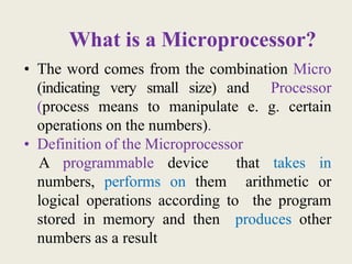
  • 1. What is a Microprocessor? • The word comes from the combination Micro (indicating very small size) and Processor (process means to manipulate e. g. certain operations on the numbers). • Definition of the Microprocessor A programmable device that takes in numbers, performs on them arithmetic or logical operations according to the program stored in memory and then produces other numbers as a result
  • 2. Difference between: – Microcomputer – a computer with a microprocessor as its CPU. Includes memory, I/O etc. – Microprocessor – A silicon chip which includes ALU, registers (as a small internal memory) & a control unit. A general purpose device (i.e. may be used for different purposes in different applications e.g. as a CPU in a microcomputer)  Uses Memory, I/O functions etc external to the chip  Configuration of the system is flexible – Microcontroller - A silicon chip which includes microprocessor, memory & I/O etc & other peripheral functions all integrated on a single chip.  More application specific, single purpose Especially used in embedded systems  Fixed configuration (i.e. fixed memory & other functions)
  • 3. Memory OutputInput A Microprocessor-based system A microprocessor based system (e.g. a microcomputer) consists of the following components:
  • 4. • Internally, the microprocessor is made up of 3 main units. – The Arithmetic/Logic Unit (ALU) – The Control Unit. – An array of Registers as a small internal memory for holding data while it is being manipulated or processed. ALU Register Array Control Inside a Microprocessor
  • 5. Memory of Microprocessor • Inside (very small) – The registers inside the microprocessor • Outside – Read Only Memory (ROM) • used to store information that does not change – Random Access Memory (RAM) • used to store information supplied by the user such as programs and data.
  • 6. 8085 Microprocessor • One of the most popular 8-bit general purpose µp launched by Intel, USA in 1976 • An N-MOS chip with 40 pins & +5V supply • Capable of addressing 216 = 64 KB of memory • It works on 3 MHz clock. • It has multiplexed address and data bus (AD0-AD7) to reduce hardware (no. of pins) on the chip • It has 74 basic instructions (formats) with 5 different addressing modes.
  • 7. Frequency Generator is connected to these pins Power Supply: +5 V Address latch Enable (to activate latch to store address Read Write Input/Output/ Memory Multiplexed Address/Data Bus (Bidirectional) Address Bus (Unidirectional) To connect slow peripherals Interrupts For DMA Request For Serial data communication
  • 8. Similar function pins are grouped in this figure- (called functional pin diagram)
  • 9.  AD0-AD7: Lower order bidirectional multiplexed Address/Data lines.  A8-A15: Higher order unidirectional address lines, carries only address  ALE: A pulse output signal from this pin is used by microprocessor to enable an 8-bit external latch to save the lower order address bits  S0,S1: These output status signals are used to indicate type of operation  RD: MP reads data from memory/IO device when this pin is active (low)  WR: MP writes data into memory/IO device when this pin is active (low)  READY: This pin is used by slow-responding peripheral devices to indicate the µP whether they are READY to send/accept data to/from µP  TRAP: A highest priority , non mask able vectored interrupt. After TRAP, restart occurs and execution starts from predefined vector address 0024H  RST5.5,6.5,7.5:These are maskable, vectored interrupts and have lower priority than TRAP  INTR: INTR is a lowest priority non-vectored which can be used to connect upto 8 peripheral devices by using an interrupt controller  INTA: An interrupt acknowledge signal pin for INTR, only acknowledgment pin among all interrupts PIN FUNCTIONS
  • 10.  HOLD & HLDA: When a peripheral device wants to gain control of system buses (e.g. for a DMA operation), it sends request to µP via this input pin. In response, µP activates HLDA (output) to acknowledge the request & temporarily releases control over system buses.  IO/M: This output control pin is used to indicate whether the read/write operation being performed by microprocessor is for memory (when low) or for I/O device (when high)  RESET IN: This control input signal connected to external RESET button to bring µP in initial standby mode. It restarts µp to memory location 0000H.  RESET OUT: When high, this indicates µP has been reset  SID & SOD: These pins are used for serial data communication by using making use of SIM & RIM instructions  X1X2 :These are clock input signals which are connected to external oscillator of 6 MHz frequency which is divided by 2 internally in 8085 to generate 3 MHz operating frequency .  CLK (out): Used to provide same 3MHz clock to the rest of the system  VCC, VSS & GND: Power supply pins VCC= +5V & VSS=GND=0V PIN FUNCTIONS
  • 11. Architecture of 8085 Microprocessor
  • 12. Functions of various building blocks: ALU: Arithmetic & Logic Unit contains digital circuitry to perform all arithmetic & logical operations in 8085 TIMING & CONTROL UNIT: Generates various types of control signals to direct microprocessor what & when a task is to be performed. INSTRUCTION DECODING & MACHINE CYCLE ENCODING: Used to decode instruction opcode into binary form & to control various machine cycle operations during execution of an instruction SERIAL I/O CONTROL: Used to control serial data communication with external devices via SID/SOD lines INTERRUPT CONTROL: Used to handle various incoming interrupts which occur via 5 interrupt pins TRAP, RST7.5, RST6.5, RST5.5 & INTR lines INCREMENTER/DECREMENTER ADDRESS LATCH: It increments/ decrements contents of Program Counter or Stack Pointer when instructions related to them are executed. ADDRESS & DATA BUFFERS: These are used to momentarily hold the 16 ‘in-transit’ address bits while they are being placed on Address/Data bus. These effectively act as an ‘interface’ between internal & external buses.
  • 13. GENERAL PURPOSE REGISTERS (B,C,D,E,H,L): These 6 register can be used singly to store any 8-bit data or as register pairs (valid pairs are B-C, D-E & H-L) to perform 16-bits operations. TEMPORAY REGISTERS (W, Z & TR): Used internally by 8085 to temporarily store 8-bit data (or partial results) while performing various arithmetic operations. Not available to user ACCUMULATOR: An 8 bit register having some special features (usually included in ALU block). It stores results of arithmetic & logical operations. Many instructions in 8085 are Accumulator-based. INSTRUCTION REGISTER: An 8-bit register used to hold opcode of the instruction currently being executing PROGRAM COUNTER: Holds 16-bits address of the next byte to fetched during execution of an instruction & is incremented by 1 each time a byte is fetched to point to the next memory location. STACK POINTER: A 16-bits register which holds the address of topmost memory location of stack. It decrements/increments by 2 each time a PUSH/POP operation is performed FLAG REGISTER: An 8 bit register whose individual bit are set/reset according to status of result generated by ALU.
  • 14. S Z X AC X P X CY S: Sign flag is set when result of an operation is negative (leftmost bit is 1 in signed arithmetic operations) Z: Zero flag is set when result of an operation is zero otherwise reset AC: Auxiliary carry flag is set when there is a carry out of 3rd to 4th bit in an 8-bit operation CY: Carry flag is set when there is a final carry generated in an operation. P: Parity flag is set when result contains even number of 1’s (Reset for odd number of 1’s ) Program Status Word: The combined 16-bits contents of Accumulator & Flag register (A & F) are named as PSW FLAG REGISTER Set = 1, Reset = 0 Accumulator (8-bits) Flag Register (8-bits) PSW (16 bits)
  • 15. Procedural steps of an example instruction (MOV C, A) (Hexcode: 4F) being fetched & executed by microprocessor from memory location 2005: Step 1: 8085 places 16-bits address (2005H) from program counter on address bus Step 2: Control unit activates RD signal to enable memory chip (RAM) Step 3: Instruction byte (4F) is placed by memory on data bus Step 4: Instruction is decoded by Instruction decoder in binary form which directs timing & control unit to generate appropriate control signals to carry out the task as specified by the instruction INSTRUCTION FETCH & EXECUTION OPERATION IN 8085
  • 16. • AD7-AD0 lines serve dual purpose; they work in time- shared mode: at one time they carry address & data at other time, to save 8 extra pins on the chip • For a read/write operation from memory, we must provide complete 16-bit address for full duration (3 clock periods) of read/write cycle (until data is loaded to/from memory. • The 8 higher-order bits of the address remain on the bus for full read/write cycle, but low-order bits remain for only 1 clock period (to make data bus free to carry data later). So we use an external 8-bit latch (a chip) to save & hold lower-order address for the remaining time (2 clock periods) or else it (lower order address) would be lost. • We use ALE control signal to activate (to save lower order address) latch in the first clock period. Multiplexing/Demultiplexing AD7-AD0
  • 17. A15-A8 LatchAD7-AD0 D7- D0 A -A7 0 8085 ALE WR RD IO/M CS Memory Chip RD WR A9-A0 A15-A10 Chip Selection Circuit Multiplexing/Demultiplexing AD7-AD0 Activated for a read (IN) operation Activated for a write (OUT) operation Activated in the first clock cycle (T1) to save lower order address in latch Latch provides address to memory for remaining time IN OR OUT
  • 18. The 8085 Instructions (Summary) The 8085 instructions can be categorized into 5 different groups: • Data Transfer • Arithmetic • Logic • Branch • Machine Control
  • 19. DATA TRANSFER GROUP MOV Rd, Rs : Copy Rs to Rd MOV R/M, M/R: Copy contents of M (addressed by HL) to R or vice versa MVI R, data (8): Move 8-bit immediate data to R MVI M, data (8): Move 8-bit immediate data to M LXI Rp, data (16): Move 16-bit immediate data to Rp LDA addr: Copy contents of given memory address to A STA addr: Copy contents of A to given memory address LHLD addr: Copy contents of given+next address to L,H respectively SHLD addr: Copy contents of L,H to given+next address respectively LDAX Rp : Copy contents of location addressed by Rp to A STAX Rp: Copy contents of A to location addressed by Rp XCHG: Exchange contents of HL & DE
  • 20. ARITHEMATIC GROUP ADD/SUB R: A+R/A-R, result in A ADD/SUB M: A+M/A-M, result in A, M addressed by HL ADC/SBB R: A+R+CY/A-R-CY, result in A ADC/SBB M: A+M+CY/A-M-CY, result in A ADI/SUI, data (8): A+data/A-data, result in A ACI/SBI, data (8): A+data+CY/A-data-CY, result in A DAD rp: HL+Rp, result in HL INR/DCR R: R+1/R-1 INR/DCR M: M+1/M-1, M addressed by HL INX/DCX Rp: Rp+1/Rp-1 DAA: Produces result in BCD (or decimal) form, instead of usual hexadecimal. Can be used immediately after any of the addition type instruction in any program for this purpose, but not usable after any subtraction instruction
  • 21. LOGICAL GROUP ANA/ ORA / XRA R: AND/OR/EX-OR A with R, result in A ANA/ORA/XRA M: AND/OR/EX-OR A with M, result in A ANI/ORI/XRI, data (8): AND/OR/EX-OR A with data, result in A CMP R: A-R, only flags changed as per result, then result discarded CMP M: A-M, only flags changed as per result, then result discarded CPI, data (8): A-data,only flags changed as per result, then result discarded STC: Set (change to 1 if not already) the carry (CY) flag CMC: Complement (0 to 1 or vice versa) the carry (CY) flag CMA: Complement (0 to 1 or vice versa) the Accumulator RAL/RAR: Rotate Accumalor left/right by 1 bit through carry (CY) flag RLC/RRC: Rotate Accumalor left/right by 1 bit, also copy 7th bit of A to CY
  • 22. BRANCH CONTROL GROUP Jump: Program counter is loaded with (jumps to) given address, doesn’t return back  Unconditional: JMP addr: Jump to given address unconditionally  Conditional: JZ/JNZ/JC/JNC/JP/JM/JPE/JPO addr: Jump to given address depending on corresponding flag condition Call: Program counter jumps to given address, saves address of next instruction in the stack, returns back (redirected by RET instruction) after execution of a subroutine which is stored at the given address  Unconditional: CALL addr: Jump to given address unconditionally, return back after execution of subroutine  Conditional: CZ/CNZ/CC/CNC/CP/CM/CPE/CPO addr: Jump to given address depending on corresponding flag condition, returns back after execution of subroutine Return: Program counter is loaded with return address that was saved in the stack at the start of CALL instruction . Last instruction of a subroutine is always a return instruction to redirect the microprocessor back to the main program  Unconditional: RET: Retrieves saved return address from the stack back to the PC  Conditional: RZ/RNZ/RC/RNC/RP/RM/RPE/RPO: Retrieves saved return address from stack back to the PC depending on the corresponding flag condition RSTn (Total 8 instructions from RST0 to RST7 for n= 0 to 7): An unconditional CALL instruction but with predefined address (8 different addresses for n=0 to 7)
  • 23. I/O, STACK & MACHINE CONTOL GROUP IN port-addr (8): Copy 8-bit data available at 8-bit input port address to A OUT port-addr (8): Copy contents of A to given 8-bit output port address PUSH Rp: Store contents of given Rp in top two locations of stack POP Rp: Load Rp with contents of top two locations from stack PUSH PSW: Store 16-bit contents of PSW (contents of A & flag register) into top two locations of stack POP PSW: Load 16-bit contents of top two locations of stack into PSW (A & flag register) XTHL: Exchange contents of HL with top two locations of stack SPHL: Copy contents of HL to stack pointer EI/DI: Enables/Disables all maskable interrupts SIM/RIM: Explained earlier NOP: No operation performed, used to provide delay in some programs HLT: Halts the program
  • 24. INSTRUCTION WORD SIZE IN 8085 • One-Byte Instructions: Occupies 1 byte in the memory, no 8/16 bits data is included in the instructions Examples: MOV A, B ADD B RAL MOV C, M CMC STC CMP M ANA B INR C • Two-Bytes Instructions: Occupies total 2 bytes in the memory, 8-bits data is included in the instructions Examples: MVI A, 05 IN 02 CPI 03 • Three-Bytes Instructions: Occupies total 3 bytes in the memory, 16-bits data is included in the instructions Examples: LXI H, 2500 LDA 3050 LHLD 2600
  • 25. 8085 ADDRESSING MODES Addressing Mode: An addressing mode indicates the location of operand in an instruction 1. IMMEDIATE: Operand itself is immediately given in the instruction Examples: MVI A,05H LXI H, 2050H ADI 02 2. DIRECT: 16 bits address (or 8 bit in case of I/O instructions) is directly given in the instruction itself Examples: LDA 2500H IN 06 SHLD 2605 OUT 03 3. REGISTER: Operand is given in one of the registers Examples: MOV B,C DCR C SUB D ANA H ADD B 4. REGISTER INDIRECT: 16-bits address of operand is indirectly provided in one of the register pairs Examples: MOV A, M ADD M INR M LDAX B STAX D 5. IMPLICIT (or IMPLIED): Operand is in the Accumulator Examples: RAL CMA RRC RLC
  • 26. MACHINE CYCLES & TIMING DIAGRAMS Instruction Cycle: Total time required to execute an instruction. Includes opcode fetch & execution cycles Machine Cycle: Time required by µP to complete one operation (read/write/fetch) of accessing memory or I/O devices during execution of an instruction. Machine cycles are of fetch, memory read/write & I/O read/write type. First machine cycle is always an opcode fetch cycle in an instruction cycle. An instruction in 8085 may have minimum 1 (which is a fetch cycle) to a maximum of 5 machine cycles depending on type of instruction. T-State: A subdivision of an operation (read/write/fetch) carried out in one system clock period. In 8085, while a fetch cycle in all instructions requires 4 T-states, other machine cycles may require minimum 3 to a maximum of 6 T-states depending upon type of instruction. Timing Diagram: A timing diagram is a graphical representation of various control signals generated during execution of an instruction. It depicts status of important control signals in each T-state of all machine cycles involved in the execution of an instruction.
  • 27. Machine cycle 2 Machine cycle 5 Instruction cycle Machine cycle1 T – State 1 T – State 2 T – State 3 T – State 6 Execution Cycle (MR/MW/IOR/IOW) Opcode Fetch Cycle 1 T-State= 1 Clock cycle INSTRUCTION CYCLE, MACHINE CYCLE, FETCH CYCLE, EXECUTION CYCLE 4 T-states
  • 28. No. of m/c cycles reqd. 1 2 3 4 5 CALCULATION OF MACHINE CYCLES Example Instructions MOV A, B HLT STC CMA XCHG INR C NOP SIM MVI A, 05 MOV B, M LDAX B ADD M RET LXIH, 2000 MVI M, 79H JMP 3050 IN 01 RSTn LDA 2500 STA 3501 CALL 2601 LHLD 2300 XTHL SHLD 3600
  • 29. ALE RD WR IO/M T1 T2 T3 T4 Some Instructions require only 1 machine cycle which is an opcode fetch cycle For Example: MOVA, B stored at 2000H in any program Opcode (or Hex code) is: 78H Note: A fetch cycle always requires 4 T-states CLK A15-A8 TIMING DIAGRAM: OPCODE FETCH CYCLE AD0-AD7 20H 78H00H INOUT S0 & S1 control signals may also be shown in the above & all other timing diagrams. They may be shown separately or combined with IO/M
  • 30. 01H 45H 25H 00H 3EH RD IO/M Op-Code Fetch Cycle Memory Read Cycle T1 T2 T3 T4 T5 T6 T7 25 Instruction: MVIA, 45H stored at 2500H location Hex Codes: 3E, 45H WR ALE A8- A15 Example Timing Diagram of an instruction requiring 2 machine cycles AD0 -AD7 CLK  A memory read cycle is exactly equal to fetch cycle except it requires 1 extra T- state & also S0=0
  • 31. Example Timing Diagram of an instruction requiring 3 machine cycles Instruction: LXI H, 2035H stored at 3010H. Hex Codes: 21H, 35H, 20H T1 T2 T3 T4 T5 T6 T7 T8 T9 T10 21H 11H 35H 12H 20H 30H 30H 30H ALE RD WR IO/M 10H Op-Code Fetch Cycle Memory Read Cycle Memory Read Cycle IN OUT IN OUT INOUT A8- A15 AD0 -AD7
  • 32. L Reg Content Of M00H 7EH ALE RD WR IO/M Op-Code Fetch Cycle Memory Read Cycle T1 T2 T3 T4 T5 T6 T7 Content Of Reg H26H MOVA, M stored at 2600H Hex Code: 7E Another example of an instruction requiring 2 machine cycles INOUT OUTIN A8- A15 AD0 -AD7
  • 33. LReg Content of RegA00H 7EH ALE RD WR IO/M Op-Code Fetch Cycle Memory Write Cycle T1 T2 T3 T4 T5 T6 T7 Content Of Reg HA0H IN OUTOUTOUT AD0 -AD7 A8- A15 MOV M, A stored at 2600H Hex Code: 77H Another example of instruction requiring 2 machine cycles
  • 34. STACK & SUBROUTINES (ILLUSTRATION OF PUSH/POP AND CALL/RET INSTRUCTIONS)
  • 35. THE STACK What is Stack? • The stack is a group of memory locations set aside by user in memory area for temporary storage (i.e. it is a portion of RAM itself) because 8085 has limited no. of registers. In addition, it has some special features. • Starting address of stack (initialization of stack) is defined by user by loading a 16-bit address into Stack Pointer as below: LXI SP, XXXX where XXXX is any 16-bits address chosen by user When is Stack used? 1. Stack is used to save the return address of Program Counter when:  A CALL/RSTn instruction (a software interrupt) encounters in a program  A hardware interrupt occurs during execution of a program In any of the above cases: i) µP executes the current instruction at hand & saves address of the next instruction (i.e. contents of PC, the return address) in stack so that it knows where it was before jumping to the subroutine/ISR of the respective interrupt.
  • 36. ii) Microprocessor loads PC with starting address of subroutine (in case of a CALL instruction) or ISR (in case of a hardware interrupt) iii) Microprocessor executes respective subroutine/ISR iv) Microprocessor retrieves back the saved return address from the stack (by using RET instruction, which is the last instruction of all subroutines) and loads back it into PC. v) Microprocessor re-continues the main program as usual  In the above cases, use of stack is made by µP internally. User only defines its starting address 2. Stack can also be used by user ‘manually’ to temporarily store the contents of a register pair (& not a single register) so that it be used for other operations or purposes. For example, consider HL pair has some specific address or data stored in it at the start of a program. Now a user wants to ‘free’ the HL pair for using in some other instructions in the program but at the same time doesn’t want to lose the initial contents. For this, he can save contents of HL pair in stack, use HL pair in other instructions & then get back saved contents from stack. Storage (called PUSHing) & retrieval (called POPing) of any contents to/from stack is achieved by using PUSH & POP instructions respectively.
  • 37. STACK PRINCIPLES • The storage and retrieval of any content on the stack follows the Last-In- First-Out (LIFO) sequence. • The stack normally grows backwards into memory • Stack Pointer is a 16-bits register located in 8085 chip, which holds the address of topmost location (called Stacktop) of stack. The contents of SP are decremented/incremented by 1 with storage/retrieval of a each byte into stack • Although stack can be initialized anywhere in the memory area, usually it is initialized at the highest available memory location so that chances of interference between stack locations & user program are minimized because address in Stack Pointer is decremented with each byte storage into stack i.e. stack will grow backwards into memory (towards user program) • The first location available for a write (or PUSH) operation in stack is one that is addressed by SP-1 & not the SP. However, the first location for a read (or POP) operation is one that is addressed by SP. During PUSHing, the stack operates in a “Decrement then Store” style i.e. decrement SP first then store at the new (lower) location address as indicated by SP. During POPing, the stack operates in a “Use then Increment” style i.e. read the contents of topmost location (addressed by SP) first & then increment it to indicate towards a new (higher) topmost location.
  • 38. EXAMPLE OF PUSH/POP INSTRUCTIONS Consider the following program: 2000 LXI SP, 2099H 2003 LXI H, 42F2H 2006 PUSH H … … … 2010 POP D … … Load SP with an arbitrary address, say 2099, to initialize stack Load any 16 bit value in the HL register pair, say 42F2 The content of the HL register pair are pushed (written) into stack. Contents of H (42H) are stored first in the location addressed by SP- 1* i.e. 2098 (higher location for higher register) & contents of L (F2H) are stored then in SP-2 i.e. 2097 (lower location for lower register). New address in SP after the PUSH operation is 2097. Contents of two locations from stack are loaded into DE pair. The 1st location is addressed by SP** (now containing 2097) & the 2nd location is addressed by SP+1 (2098). So, E is loaded first with F2H & then D is loaded with 42H. New address in SP after this POP operation is 2098. Note: *As mentioned earlier, the first available location for storage in the stack is always SP- 1 (2098 in the above example). Also, because a PUSH instruction copies contents of a register pair (HL, BC or DE), it requires two (consecutive) memory locations in the stack. ** As mentioned earlier, the first memory location that is readable from stack is SP (=2097 here, after execution of PUSH instruction). Also, because a POP instruction loads a register pair, it reads two locations (bytes) from the stack
  • 39.  The SP is decremented by one to 2098H, & the contents of the H register (42H) are copied to memory location 2098H  The SP is again decremented by one to 2097H & the contents of the L register (F2H) are copied to memory location 2097H  New SP contents after PUSH operation are 2097 Execution of PUSH H 42 F2 Flag C E L A B D H SP F2 42 X 2097 2098 2099 2097 8085 Registers Stack Execution of PUSH H instruction, as explained in the previous example, is illustrated here: Contents of SP & stack locations after PUSH H operation
  • 40.  The contents (F2H) of the current stacktop location (2097H) are copied to E register and the SP is incremented by one to 2098H  The contents of the new top location (2098H) of the stack are copied to D register, and the SP is incremented by one again  Address of new topmost location (contents of SP) now becomes 2099H after the POP operation 42 F2 2099 F C E L A B D H SP 8085 Register Execution of POP D Contents of SP & stack locations after POP D operation Execution of POP D instruction, as explained in the previous example, is illustrated here: F2 2097 42 2098 X 2099 Stack
  • 41. PUSH PSW instruction is similar to PUSH Rp instruction except that it stores PSW (the 16-bits combined contents of Accumulator & Flag Register) instead of a general purpose register pair into the stack 12 80 80 12 X FFFB FFFC FFFE FFFF PUSH PSW Stack A (8) Flag(8) For example assume Accumulator & Flag registers contain 12H & 80H respectively. Assume stack is initialized at FFFFH (i.e. contents of SP) then on execution of PUSH PSW:  SP is decremented by one & the contents of Accumulator (12H) are copied first to the FFFEH location  SP is decremented by one again & the contents of Flag register (80H) are copied then to the FFFDH location  New contents of SP are FFFDH after the PUSH PSW operation. Contents of SP & PSW after PUSH PSW operation FFFDSP
  • 42. POP PSW instruction is similar to POP Rp instruction except that it reads contents of top two locations from the stack & loads them into PSW (or Accumulator & Flag Register) 12 80 80 12 X FFFB FFFC FFFD FFFE POP PSW Stack A FContinuing with example of PUSH PSW explained earlier, we assume that current address in SP is FFFDH having value 80H. Then, on execution of POP PSW following actions take place in steps:  Contents of top location addressed by SP (i.e. 80H) are copied to the Flag register first.  SP is incremented by one & the contents of current top location (now FFFEH) are copied to the Accumulator.  SP is incremented by one again & the contents of current top location now become FFFFH. SP FFFF Contents of SP & PSW after POP PSW operation
  • 43.  A subroutine is group of instructions (a subprogram) written separately from the main program to perform a function that occurs repeatedly in the main program  When a main program CALLs a subroutine, the program execution is transferred to the subroutine. After the completion of the subroutine ,the program execution returns to the main program.  The microprocessor uses stack to store the return address.  8085 has two instructions for dealing with subroutines: – The CALL instruction, used to redirect program execution to the subroutine. Format of CALL instruction is: CALL XXXX (where XXXX is 16-bits starting address of the subroutine) A CALL instruction may be of conditional or unconditional type – The RET instruction, used to return to the main program at the end of the subroutine. No address is provided by user in a return instruction as it automatically retrieves return address from the stack top locations. RET may also be of conditional or unconditional type  A CALL instruction is always used in conjunction with RET instruction SUBROUTINE
  • 44. EXECUTION OF CALL/RET INSTRUCTIONS Following sequence of actions take place in when microprocessor encounters a CALL instruction in the middle of a program (same steps are taken by microprocessor when a hardware interrupt occurs in the middle of program):  Microprocessor saves the address of next instruction (i.e. contents of PC, the return address) in the stack so that it knows where it was before jumping to the subroutine.  Microprocessor loads PC with 16-bits starting address (provided in the instruction ) of the subroutine  Microprocessor executes the subroutine  Microprocessor retrieves back the saved return address from the stack (by using RET instruction, the last instruction of subroutine) and loads back it into the PC Microprocessor re-continues the main program as usual
  • 45. 2000 …. 2001… 2002 … 2003 CALL 3000 2006 … 2007 … 2008 ... 2009 CALL 3000 200C … 200D … … … 3000 .… 3001 …. 3002 …. …. …. RET Consider the following situation in which microprocessor is executing a (main) program (stored at 2000H onwards in RAM) & faces CALL instructions at 2003H & 2009H locations. Assuming subroutine is stored 3000H onwards, microprocessor saves address of next instructions (2006H & 200CH respectively) in the stack, loads starting address (3000H) of subroutine into PC & executes the subroutine. At the end of the subroutine, RET instruction instructs microprocessor to retrieve the saved return addresses which are then loaded back into PC & thus microprocessor continues the main program as before. Main Program Subroutine
  • 46. 8085 INTERRUPTS • An interrupt is a hardware or software initiated subroutine CALL. • An interrupt is considered to be an emergency signal that is serviced by the Microprocessor as soon as possible. • What happens when MP is interrupted ? When microprocessor receives an interrupt signal, it suspends the currently executing program and jumps to a new memory location (interrupt vector) to execute an Interrupt Service Routine (ISR) in response to the incoming interrupt. There are two ways of redirecting the execution to the ISR depending on whether the interrupt is vectored or non-vectored. Vectored: The address of the subroutine is already known to the microprocessor Non Vectored: The external device supplies the address of the subroutine to the Microprocessor  Interrupts are also categorized as SOFTWARE & HARDWARE interrupts. In 8085: SOFTWARE Interrupts: RST n & CALL instructions HARDWARE Interrupts: TRAP, RST 7.5, 6.5, 5.5, INTR
  • 47.  An interrupt vector is a pointer or memory address where the ISR is stored in the memory  All interrupts are mapped onto a particular memory area called the Interrupt Vector Table (IVT) which shows vector addresses for each interrupt  For each type of interrupt, a unique ISR is written at respective vector locations which directs microprocessor to take some predefined action (s)  An RSTn instruction is equivalent to a CALL instruction but with a fixed address & occupies only a 1byte as compared to 3bytes by a CALL instruction Pin or interrupt Predefined Vector addresses for 8085 hardware interrupts TRAP 0024 RST 5.5 002C RST 6.5 0034 RST 7.5 003C INTR * * the address of the ISR is determined by the external hardware (or interrupt controller) RSTn Instruction Equivalent to RST0 CALL 0000H RST1 CALL 0008H RST2 CALL 0010H RST3 CALL 0018H RST4 CALL 0020H RST5 CALL 0028H RST6 CALL 0030H RST7 CALL 0038H
  • 49. Execution of an Interrupt Upon receiving an Interrupt signal, microprocessor saves the memory location of the next instruction on the stack and the program is transferred to a new memory location specified by its vector address where microprocessor executes an ISR. All other maskable interrupts are automatically disabled until current interrupt is attended  An ISR is a predefined set of instructions (a subprogram) which performs a specific task. It must include the EI instruction in one of the ending instructions so that all interrupts are re-enabled for coming in future  Last instruction of an ISR must always be an RET instruction which instructs microprocessor to retrieve the saved return address from the stack so that program is transferred back to where the program was interrupted.
  • 50. COMPARISON OF 8085 HARDWARE INTERRUPTS Interrupt Name Priority Maskable Masking Method Vectored Triggering Method INTR Lowest Yes DI / EI No Level Sensitive RST 5.5 / RST 6.5 Yes DI / EI SIM Yes Level Sensitive RST 7.5 Yes DI / EI SIM Yes Edge Sensitive TRAP Highest No None Yes Level & Edge Sensitive
  • 51.
  • 52. SIM Instruction SDO SDE XXX R7.5 MSE M7.5 M6.5 M5.5 RST5.5 Mask RST6.5 Mask RST7.5 Mask }0 –Available (not masked) 1 - Masked Mask Set Enable 0 - Ignore bits 0-2 1 - Set the masks according to bits 0-2 Force RST7.5 Flip Flop to resetNot Used Enable Serial Data 0 - Ignore bit 7 1 - Send bit 7 to SOD pin Serial Data Output While EI/DI instructions enable/disable all maskable interrupts at once, SIM instruction can be used to selectively mask (or disable) 3 out of 4 maskable interrupts which are RST7.5,RST6.5 & RST5.5. Fourth maskable interrupt INTR can only be enabled/disabled by using EI/DI instructions. SIM instruction can be used to perform two different tasks: 1. For masking of 3 interrupts 2. For serial data transmission (Each time a SIM instruction is executed, 7th bit of Accumulator is automatically copied to SOD pin of 8085)
  • 53. Example of how to use SIM instruction in any program Example problem:- Set the interrupt masks so that RST5.5 is enabled, RST6.5 is masked & RST7.5 is enabled. • We can determine the bit pattern as per format of SIM instruction given below: SDO SDE XXX R7.5 MSE M7.5 M6.5 M5.5 - Enable 5.5 - Disable 6.5 - Enable 7.5 - Allow setting the masks - Don’t reset the flip flop - Bit 5 is not used - Don’t use serial data - Serial data is ignored bit 0 = 0 bit 1 = 1 bit 2 = 0 bit 3 = 1 bit 4 = 0 bit 5 = 0 bit 6 = 0 bit 7 = 0 0 0 0 0 1 0 1 0 Contents of accumulator are: 0AH EI MVI A, 0A SIM • Now use following set of instructions to implement required masks using SIM  First of all enable all interrupts using EI instruction without using which SIM wouldn't be effective  Move the prepared bit pattern (0AH here) to Accumulator  SIM instruction interprets contents of Accumulator same as per the above format & performs the desired operation of masking the respective interrupts
  • 54. RIM instruction SDI P7.5 P6.5 P5.5 IE M7.5 M6.5 M5.5 7 6 5 4 3 2 1 0 RST5.5 Mask RST6.5 Mask RST7.5 Mask } Indicate current masking status of interrupts set by user (using SIM) 0 -Available 1 - Masked Status of Interrupt Enable Flip Flop: 1 Set 0 Reset Serial Data In RST5.5 Interrupt Pending RST6.5 Interrupt Pending RST7.5 Interrupt Pending Like SIM instruction, RIM can be used to perform two different tasks: 1. To read current status of 3 maskable interrupts 2. For serial data reception (Each time a SIM instruction is executed, the bit present on SID pin of 8085 is automatically moved to 7th bit of the Accumulator) Pending Interrupts: Since the 8085 has 5 interrupt lines, another interrupts may occur while an interrupt is being attended and thus remain pending. Such interrupts are called pending interrupts & would be attended as soon as ISR of current interrupt is executed. A programmer may know the status (current value of high/low on the respective interrupt pin) of such interrupts anytime by using RIM instruction.
  • 55. An example of Memory Mapping & Address allocations in 8085 The memory map is a pictorial representation of the memory address ranges of different memory chips (for example 5 no. of chips here) of different sizes and shows where they are located within the full address range available. 0000 AddressRange EPROM RAM 1 RAM 2 RAM 3 RAM 4 0000 8FFF 9000 A3FF A400 Address Range of EPROM Chip 3FFF 4400 Address Range of 1st RAM Chip 5FFF 6000 Address Range of 2nd RAMChip Address Range of 3rd RAMChip Address Range of 4th RAMChip F7FF FFFF