
Recommended
Recommended
More Related Content
What's hot
What's hot (20)
Similar to Creating an Embedded System Lab
Similar to Creating an Embedded System Lab (20)
Recently uploaded
Recently uploaded (20)
Creating an Embedded System Lab
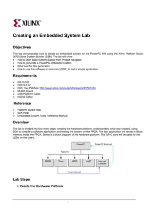
- 1. Creating an Embedded System Lab Objectives This lab demonstrates how to create an embedded system for the PowerPC 405 using the Xilinx Platform Studio (XPS) Base System Builder (BSB). The lab will show • How to start Base System Builder from Project Navigator • How to generate a PowerPC embedded system • What are the files generated • How to use the software environment (SDK) to test a simple application Requirements ISE 9.2.04 EDK 9.2.02 EDK Tool Patches: http://www.xilinx.com/support/answers/29702.htm ML403 Board USB Platform Cable RS232 Cable Reference Platform Studio Help SDK Help Embedded System Tools Reference Manual Overview The lab is divided into four main steps: creating the hardware platform, understanding what was created, using SDK to compile a software application and testing the system on the FPGA. The test application will reside in Block memory inside the FPGA. Below is a block diagram of the hardware platform. The GPIO core will be used for the LEDs on the board. PowerPC PowerPC Interrupt PLB v46 BRAM Timer GPIO UART Interrupt Controlle r Timer Interrupt Lab Steps I. Create the Hardware Platform 1
- 2. We will use Base System Builder to create the platform for the design. The Wizard can quickly create baseline systems for current development boards or for custom boards. The system will include a timer, an Interrupt Controller, a UART Lite, a GPIO controller for the LEDs, and internal Block RAM memory. 1. Start Xilinx ISE Project Navigator and start a new project: File > New Project… 2. Select a project name and location. There should be no spaces in the directory path. Click Next. 3. Select Virtex-4, XC4VFX12, FF668, -10. For this lab, pick VHDL as the Preferred Language. Click Next. 4. Select New Source… then select Embedded Processor. Type ppc_system for the File name. Click Next. Click Finish then OK. 5. Click Next until the Project Summary window then Finish. 6. A message will appear asking if you want to create a Base System using the BSB wizard, click Yes. 7. In the Welcome window click Next to create a new design. 8. Select the Xilinx Virtex-4 ML403 Evaluation Platform from the list of available Xilinx boards and select Revision 1. Click Next 9. In the Select Processor window, PowerPC is selected. Click Next. 10. Configure the processor: • 100MHz for all clocks, FPGA JTAG, no On-Chip memory (OCM). Click Next. 11. Configure IO Interfaces: • XPS UARTLITE (9600, no parity) for the RS232_Uart, XPS GPIO (4-bits) for the LEDs_4Bit, deselect all others. Click Next. • Deselect all peripherals in the Configure IO Interfaces windows. Click Next. 12. In the Add Internal Peripherals window, change the memory size to 64KB then click on Add Peripheral… Add an XPS TIMER: • XPS TIMER (32-bit counter, 1 timer, use interrupt). The interrupt controller will be added automatically when the use interrupt option is selected. Click Next. 2
- 3. 13. In the Software Setup window, uncheck Memory Test then click Next. 14. In the Configure Peripheral Test Application window, click Next. 15. Click on the Generate button to generate the project. Click on Finish. II. Understanding the System The Base System Builder wizard created all the files needed to get started with an embedded PowerPC system. The Xilinx Platform Studio IDE has all the information for the project. We will look at the interface and the files created. 1. Xilinx Platform Studio provides an integrated environment for creating the software and hardware of an embedded processor system. It also provides an editor and a project management interface to create and edit source code. The complete hardware and software flows can be completed within XPS. Platform Studio SDK provides a more powerful software environment and will be used for the software application during the tutorials. 2. The System Assembly window shows each peripheral used and the connections between the peripherals when the Bus Interface button is selected. We will learn more about the System Assembly view as well as the IP Catalog tab in the next lab. 3
- 4. 3. The Project tab provides information on the project options used, gives access to the main Project files, and log files. The main Project Files are: • MHS File. The Microprocessor Hardware Specification file contains the hardware specification of the entire system. The MHS file contains the bus architecture used, the peripherals used, the connectivity for the system, the interrupt request priorities, and the address space. The MHS file can also call out custom IP. • MSS File. The Microprocessor Software Specification file defines the software drivers associated with peripherals, standard input/output devices, interrupt handler routines, RTOS and libraries used, and other related software features. • UCF File. The User Constraints File contains the timing and placement constraints for the FPGA. • iMPACT Command File. The download.cmd file contains JTAG chain information to download the design to the FPGA on the development board. • Implementation Options File. The fast_runtime.opt file contains implementation options for all the phases of the FPGA hardware implementation. The options are used to run the standard ISE tools. • Bitgen Options File. The bitgen.ut file provides options when generating the bit file for the FPGA. 4. The Applications tab shows the software applications available for the processor. For this lab, SDK will be used to edit and compile the software. 5. Right-click on the TestApp_Peripheral project and unselect Mark to Initialize BRAMs. 6. Right-click on Default: ppc405_0_bootloop and select Mark to Initialize BRAMs. 7. Click on the BLOCK DIAGRAM tab to view the block diagram for the project. The block shows the connections between the different busses and components in the system. 8. A datasheet of the system can also be generated. Go to Project > Generate and View Design Report to view the design report. 9. To view the general project options go to Project > Project Options… Click Cancel to close the window. 10. Go to Software > Software Platform Settings… to view the software options. The software driver version information can be viewed by selecting Drivers on the left side. These options are used when compiling libraries and BSPs. Click Cancel to close the window. 11. The UCF file needs to be added to the Project Navigator project in order to implement the FPGA design 12. In ISE go to Project > Add Copy of Source… Browse to the ppc_systemdata directory and select ppc_system.ucf. Click Open then OK. 13. Double-click on Update Bitstream with Processor Data to create the hardware bit file. III. Compiling the Test Application Using SDK Platform Studio SDK is an Eclipse based software development environment to create and debug software applications. Features include project management, multiple build configurations, a feature-rich C/C++ code editor, error navigation, a debugging and profiling environment, and source code version control. More time will be spent on the different features of the SDK in the next labs. 1. Launch SDK. In XPS, go to Software > Launch Platform Studio SDK. Click OK. 2. SDK will automatically generate the libraries and BSP for the project. A directory with the name of the processor instance will be created. Within each processor instance directory, C header files that are 4
- 5. needed by the drivers, driver functions that the particular processor can access, and intermediate files and makefiles that are needed to compile the libraries and drivers are generated. 3. Select Import XPS Application Projects then click on Next. 4. Select the TestApp_Peripheral application then click Finish. 5. The TestApp_Peripheral project was created by Base System Builder to test the project. It contains C source files to test each peripheral and a linker script. Expand the project to view the sources associated with the project. All the files are linked from their original directory. 6. To view the project properties right-click on the TestApp_Peripheral project and select Properties. The C/C++ selection contains all the build options. Click OK to exit. 7. Above the project, all the libraries and include files associated with the hardware project are available to browse. The include directory contains all the header files applicable for the current project. 8. Double click on the TestApp_Peripheral.c file to view the application. The project was compiled when imported from XPS by default if the Build Automatically option is set. You can double-click on the include directives in the right side Outline window to view the source for the headers. 9. Compile the project if not already compiled. Go to Project > Build Project. 10. Initialize the internal BRAM with the application executable. Go to Device Configuration > Program Hardware Settings… 11. Select the TestApp_Peripheral executable. Click Save. 12. The system is ready to be downloaded to the board. IV. Test the Generated System with the Sample Application 1. Connect a serial cable to the RS232 port and connect the Platform USB cable. 2. Power-up the board. 3. Open Hyperterminal and connect at 9600, no parity. 4. Download to the FPGA from SDK: Device Configuration > > Program Hardware. 5. Verify that the different peripheral print statements appear on the Hyperterminal window and that the LEDs are blinking. 6. Close SDK. 5