검토요청(차별화요소)
•Download as PPTX, PDF•
0 likes•691 views

양아치조명디자인 하는 놈때문에 사기당했던 자료들... 디자인 하는 양아치가 반도체 이론을 만든다고? 여러분 공부들 하시고 사기에 당하지 마시길...

Recommended
More Related Content
Viewers also liked
Similar to 검토요청(차별화요소)
Similar to 검토요청(차별화요소) (20)
More from Yeonmoon Jeong
Recently uploaded
Recently uploaded (20)
검토요청(차별화요소)
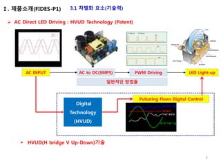
- 1. 1 Ⅰ. 제품소개(FIDES-P1) Digital Technology (HVUD) AC INPUT LED Light-up Pulsating Flows Digital Control AC to DC(SMPS) PWM Driving 일반적인 방법들 HVUD(H bridge V Up-Down)기술 AC Direct LED Driving : HVUD Technology (Patent) 3.1 차별화 요소(기술력)
- 2. P1 V Detect ambient light sensor 4개의 LED그룹으로 나누어 콘트롤함. 그 가운데 하나의 LED가 고장을 일으켜도 정상작동을 하도록 바이패스 회로를 설치함. AC Input 2 HVUD Power Block (H bridge V Up-Down Output Technology) 3.2 차별화 요소(기술력)
- 3. Ⅰ. 제품소개(FIDES-P1) Digital Technology (I-V컨트롤) AC INPUT LED Light-up Pulsating Flows Digital Control AC to DC(SMPS) PWM Driving 일반적인 방법들 AC Direct LED Driving : I-V 컨트롤 Technology 3.1 차별화 요소(기술력) I-V 컨트롤 기술은
- 4. 4 Edge Det Overlap Protect Level Shift Level Shift Level Shift LEDRV_A1 3V S R ISRPO C200 ISER SDWN DUEN SW1 SW2 IS0 IS0 V1 V1 C200 V3 3V DMO IS00 DUEN Hysteresis Saw Tooth Wave DMO V4V2 3V5V 3.0 RAMP DMO DUEN DMO 1uF 1uF 100u SW0 SW1 SW2 V6 SW0 H = Voltage boost L = Voltage down H = Shut Down L = Operation IS00 Level Shift ERAMP_IS_C2 DTENP_C4 DUDET_C1 VLED VIS0 Vf1 Vfn VRE= 0.3V VRUD= 0.3V 전압Boost/Down조건 전압Down: SW0=1, SW1=0, SW2=0 SW0=0, SW1=1. SW2=0 전압Boost: SW0=1, SW1=0, SW2=1 SW0=0, SW1=0, SW2=1 입출력상황에 따라Switch 회로동작 설명: 1. 전원투입시는전원이 서서히증가해, 그 에 응해서 LED전압인 VLED도증가 2. LED의 Vf이상 VLED가 상승하면 LED 에 전류가 흘러서 VIS0에 전압이 발생한다. 3. VIS0와 error amp의 기준전압 VRE=0.3 V와 비교해서 그 오차전압과 톱니 파로 PWM파를 만들어 Driver회로 D TENP_C4에 입력된다. 4.VISO전압은 전압 업·다운검출회로 (DUDET_C1)의기준전압VRUD와 비 교되어 VISO가VRUD보다낮으면 Low level, 높으면High Level이 출 력된다 5. DTENO_C4는 상기SW0,1,2의 동작모드 에 따라서 LED전압을 상승 또는 하 강시키고, 최종적으로는 VIS0=VRE 이 되는 시점으로 밸런스를 갖게 된 다. 다시 말해서 LED전류 VIS0/3값 으로 된다. I-V 컨트롤 블록도 3.2 차별화 요소(기술력)
- 5. FIDES : Investment Highlights This presentation contains forward-looking statements about future events, including our challenges, strategies, market Opportunities and sizes, growth rates and growth drivers of our markets. These presentation are based on our assumptions and expectations which may prove incorrect and our goals and objectives which may change. These presentation are subject to risks such as whether our target statements are subject to risks such as whether our target markets and sales grow as projected; price erosion and other competitive market pressures; controlling our expenses, and other risk factors detailed with the Securities and Exchange Commission. Due to these and other risks, our future actual results could differ materially from those discussed. We undertake no obligation to publicly release updates or revisions to these information. Jeong.osc@gmail.com Jeong.osc@gmail.com Tel : 82-10-3343-0318
- 6. TOPOLOGY • No aluminum electrolytic capacitor for unregulated DC Valley fill technology Patent • Free AC input LED load constant I-V control Patent • Zero Crossing multi discharge by small cap Patent pending • Galvanic isolation and non isolation supports • Direct MCU controlled for flicker free LED dimming • Standby zero technology patent pending • UPS function supports • All solid state designed power for MTBF guarantee • High efficiency 93% with PF0.95 over Jeong.osc@gmail.com Tel : 82-10-3343-0318 Jeong.osc@gmail.com