Vertical Deflection Booster Spec Sheet
•
0 likes•208 views

The document summarizes a vertical deflection booster integrated circuit. It can handle flyback voltages up to 90V and provides up to 2.6A of output current. It has thermal protection and can operate with power supply voltages up to 42V. The document includes application examples, electrical specifications, and packaging details.

Recommended
More Related Content
What's hot
What's hot (20)
Similar to Vertical Deflection Booster Spec Sheet
Similar to Vertical Deflection Booster Spec Sheet (20)
Recently uploaded
Recently uploaded (20)
Vertical Deflection Booster Spec Sheet
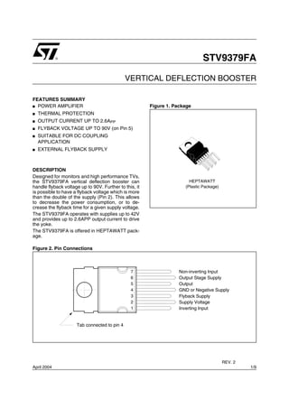
- 1. 1/9April 2004 STV9379FA VERTICAL DEFLECTION BOOSTER REV. 2 FEATURES SUMMARY ■ POWER AMPLIFIER ■ THERMAL PROTECTION ■ OUTPUT CURRENT UP TO 2.6APP ■ FLYBACK VOLTAGE UP TO 90V (on Pin 5) ■ SUITABLE FOR DC COUPLING APPLICATION ■ EXTERNAL FLYBACK SUPPLY DESCRIPTION Designed for monitors and high performance TVs, the STV9379FA vertical deflection booster can handle flyback voltage up to 90V. Further to this, it is possible to have a flyback voltage which is more than the double of the supply (Pin 2). This allows to decrease the power consumption, or to de- crease the flyback time for a given supply voltage. The STV9379FA operates with supplies up to 42V and provides up to 2.6APP output current to drive the yoke. The STV9379FA is offered in HEPTAWATT pack- age. Figure 1. Package Figure 2. Pin Connections HEPTAWATT (Plastic Package) Output Stage Supply Output GND or Negative Supply Flyback Supply Supply Voltage Inverting Input Tab connected to pin 4 7 6 5 4 3 2 1 Non-inverting Input
- 2. STV9379FA 2/9 Figure 3. Block Diagram Table 1. Absolute Maximum Ratings Note: 1. Versus Pin 4. 2. The output current can reach 5A peak for t ≤ 10µs (up to 120Hz). 3. Provided SOAR is respected (see Figures 6 and 7). Symbol Parameter Value Unit VS Supply Voltage (Pin 2) (see note 1) 50 V V6 Flyback Peak Voltage (Pin 6) (see note 1) 100 V V1, V7 Amplifier Input Voltage (Pins 1-7) (see note 1) – 0.3, + VS V IO Maximum Output Peak Current (see notes 2 and 3) 1.8 A I3 Maximum Sink Current (t < 1ms) 1.8 A I3 Maximum Source Current (t < 1ms) (in the diode, see Block Diagram) (see note 2) 1.8 A VESD ESD susceptibility : EIAJ Norm (200pF discharged through 0Ω) 300 V V3 - V2 Voltage Difference between Flyback Supply and Supply Voltage 50 V TOPER Operating Ambient Temperature – 20, + 75 °C TSTG, Storage Temperature – 40, + 150 °C Tj Junction Temperature + 150 °C 4 5 7 THERMAL PROTECTION 1 2 6 3 INVERTING INPUT NON-INVERTING INPUT OUTPUT GROUND or NEGATIVE SUPPLY OUTPUT STAGE SUPPLY SUPPLY VOLTAGE STV9379FA POWER AMPLIFIER FLYBACK SUPPLY
- 3. 3/9 STV9379FA Table 2. Thermal Data Table 3. ELECTRICAL CHARACTERISTICS (VS = 42V, TA = 25°C, unless otherwise specified) Symbol Parameter Value Unit Rth (j-c) Junction-case Thermal Resistance Max 3 °C/W Tt Temperature for Thermal Shutdown 150 °C ∆Tt Hysteresis on Tt 10 °C Tjr Recommended Max. Junction Temperature 120 °C Symbol Parameter Test Conditions Min. Typ. Max. Unit VS Operating Supply Voltage Range Versus Pin 4 10 42 V V3M Operating Flyback Supply Voltage (V3M ≤ VS + 50V) Versus Pin 4 VS 70 V I2 Pin 2 Quiescent Current I3 = 0, I5 = 0 13 20 mA I6 Pin 6 Quiescent Current I3 = 0, I5 = 0 5 10 30 mA IO Max. Operating Peak Output Current 1.3 A I1 Amplifier Bias Current V1 = 22V, V7 = 23V – 0.15 – 1 µA I7 Amplifier Bias Current V1 = 23V, V7 = 22V – 0.15 – 1 µA VIO Offset Voltage 7 mV ∆VIO /dt Offset Drift versus Temperature – 10 µV/°C GV Voltage Gain 80 dB V5L Output Saturation Voltage to GND (Pin 4) I5 = 1.3A 1 1.6 V V5H Output Saturation Voltage to Supply (Pin 6) I5 = - 1.3A 1.6 2.2 V VD5 - 6 Diode Forward Voltage between Pins 5-6 I5 = 1.3A 1.4 2.1 V VD3 - 6 Diode Forward Voltage between Pins 3-6 I3 = 1.3A 1.7 2.5 V V3-6 Voltage Drop between Pins 3-6 (2nd part of flyback) I3 = - 1.3A 2.9 3.6 V
- 4. STV9379FA 4/9 APPLICATION CIRCUITS Figure 4. AC Coupling 4 5 7 R5 R3 R2 R4 R1 1 2 6 Flyback Supply Ly Yoke Rd (*) STV9379FA 3 Ly 50µS Ly < Rd <(*) + VS VREF POWER AMPLIFIER THERMAL PROTECTION CL 0.22µF1.5Ω 20µS
- 5. 5/9 STV9379FA Figure 5. DC Coupling Figure 6. Output Transistors SOA (for secondary breakdown) Figure 7. Secondary Breakdown Temperature Derating Curve (ISB = secondary breakdown current) Vertical Position Adjustment POWER AMPLIFIER 4 5 7 R5 R2 R1 1 2 6 Flyback Supply STV9379FA 3 Ly Ly < Rd <(*) + VS VREF+ - VEE THERMAL PROTECTION 0.22µF1.5Ω Rd (*) Ly Yoke 50µS 20µS IC (A) 10 1 10-1 10-2 1 10 102 t = 1ms t = 10ms t = 100ms VCE (V) @ Tcase = 25˚C 100 90 80 70 60 25 50 75 100 ISB (%) Tcase (C˚) 125
- 6. STV9379FA 6/9 PART NUMBERING Table 4. Order Codes Part Number Package Temperature Range STV9379FA HEPTAWATT7 -25 to 85 °C
- 7. 7/9 STV9379FA PACKAGE MECHANICAL Table 5. HEPTAWATT7 - Mechanical Data Figure 8. HEPTAWATT7 - Package Dimensions Note: Drawing is not to scale Symbol millimeters inches Typ Min Max Typ Min Max A 4.8 0.189 C 1.37 0.054 D 2.4 2.8 0.094 0.110 D1 1.2 1.35 0.047 0.053 E 0.35 0.55 0.014 0.022 F 0.6 0.8 0.024 0.031 F1 0.9 0.035 G 2.41 2.54 2.67 0.095 0.100 0.105 G1 4.91 5.08 5.21 0.193 0.200 0.205 G2 7.49 7.62 7.8 0.295 0.300 0.307 H2 10.4 0.409 H3 10.05 10.4 0.396 0.409 L 16.97 0.668 L1 14.92 0.587 L2 21.54 0.848 L3 22.62 0.891 L5 2.6 3 0.102 0.118 L6 15.1 15.8 0.594 0.622 L7 6 6.6 0.236 0.260 M 2.8 0.110 M1 5.08 0.200 Dia. 3.65 3.85 0.144 0.152
- 8. STV9379FA 8/9 REVISION HISTORY Table 6. Revision History Date Revision Description of Changes June-1998 1 First Issue 14-Apr-2004 2 Stylesheet update. No content change.
- 9. 9/9 STV9379FA Information furnished is believed to be accurate and reliable. However, STMicroelectronics assumes no responsibility for the consequences of use of such information nor for any infringement of patents or other rights of third parties which may result from its use. No license is granted by implication or otherwise under any patent or patent rights of STMicroelectronics. Specifications mentioned in this publication are subject to change without notice. This publication supersedes and replaces all information previously supplied. STMicroelectronics products are not authorized for use as critical components in life support devices or systems without express written approval of STMicroelectronics. The ST logo is a registered trademark of STMicroelectronics. All other names are the property of their respective owners © 2004 STMicroelectronics - All rights reserved STMicroelectronics GROUP OF COMPANIES Australia - Belgium - Brazil - Canada - China - Czech Republic - Finland - France - Germany - Hong Kong - India - Israel - Italy - Japan - Malaysia - Malta - Morocco - Singapore - Spain - Sweden - Switzerland - United Kingdom - United States www.st.com