Hierarchy of management that covers different levels of management
Presentation1.pptx
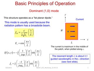
1. This mode is usually used because the
radiation pattern has a broadside beam.
10
1
2 r
c
f
L
cos
z
x
E
L
0
1
ˆ sin
s
x
J x
j L L
The resonant length L is about 0.5
guided wavelengths in the x direction
(see next slide).
x
y
L
W
Current
Basic Principles of Operation
Dominant (1,0) mode
This structure operates as a “fat planar dipole.”
1
ˆ
, sin
x
H x y y
j L L
The current is maximum in the middle of
the patch, when plotted along x.
8/3/2023 MZCET_ECE_Workshop_31-03-23 1
2. The resonance frequency is mainly controlled by the
patch length L and the substrate permittivity.
Resonance Frequency of Dominant (1,0) Mode
Comment:
A higher substrate permittivity allows for a smaller antenna (miniaturization),
but with a lower bandwidth.
Approximately, (assuming PMC walls)
This is equivalent to saying that
the length L is one-half of a
wavelength in the dielectric.
0 / 2
/ 2
d
r
L
1
k L
2 2
2
1
m n
k
L W
(1,0) mode:
Basic Principles of Operation
1 2 / d
k
8/3/2023 MZCET_ECE_Workshop_31-03-23 2
3. The resonance frequency calculation can be improved by adding a
“fringing length extension” L to each edge of the patch to get an
“effective length” Le .
10
1
2 e
r
c
f
L
2
e
L L L
Note: Some authors use effective permittivity in this equation.
(This would change the value of Le.)
Basic Principles of Operation
Resonance Frequency of Dominant Mode
y
x
L
Le
L
L
8/3/2023 MZCET_ECE_Workshop_31-03-23 3
4. Hammerstad formula:
0.3 0.264
/ 0.412
0.258 0.8
eff
r
eff
r
W
h
L h
W
h
1/2
1 1
1 12
2 2
eff r r
r
h
W
Note:
Even though the Hammerstad formula
involves an effective permittivity, we still use
the actual substrate permittivity in the
resonance frequency formula.
10
1
2
2 r
c
f
L L
Basic Principles of Operation
Resonance Frequency of Dominant Mode
8/3/2023 MZCET_ECE_Workshop_31-03-23 4
5. Note: 0.5
L h
This is a good “rule of thumb” to give a quick estimate.
Basic Principles of Operation
Resonance Frequency of Dominant Mode
8/3/2023 MZCET_ECE_Workshop_31-03-23 5
7. General Characteristics
The bandwidth is directly proportional to substrate thickness h.
However, if h is greater than about 0.05 0 , the probe inductance (for a
coaxial feed) becomes large enough so that matching is difficult – the
bandwidth will decrease.
The bandwidth is inversely proportional to r (a foam substrate gives a high
bandwidth).
The bandwidth of a rectangular patch is proportional to the patch width W
(but we need to keep W < 2L ; see the next slide).
Bandwidth
8/3/2023 MZCET_ECE_Workshop_31-03-23 7
8. 2 2
2
mn
r
c m n
f
L W
10
1
2 r
c
f
L
02
2
2 r
c
f
W
2
W L
Width Restriction for a Rectangular Patch
fc
f10
f01 f02
01
1
2 r
c
f
W
W = 1.5 L is typical.
02 10
1 1
2
r
c
f f
W L
General Characteristics
L
W
8/3/2023 MZCET_ECE_Workshop_31-03-23 8
9. Some Bandwidth Observations
For a typical substrate thickness (h /0 = 0.02), and a typical
substrate permittivity (r = 2.2) the bandwidth is about 3%.
By using a thick foam substrate, bandwidth of about 10% can be
achieved.
By using special feeding techniques (aperture coupling) and
stacked patches, bandwidths of 100% have been achieved.
General Characteristics
8/3/2023 MZCET_ECE_Workshop_31-03-23 9
10. 0 0.01 0.02 0.03 0.04 0.05 0.06 0.07 0.08 0.09 0.1
h /
0
5
10
15
20
25
30
BANDWID
TH
(%)
r
2.2
= 10.8
W/ L = 1.5
r = 2.2 or 10.8
Results: Bandwidth
The discrete data points are measured values.
The solid curves are from a CAD formula (given later).
0
/
h
10.8
r
2.2
General Characteristics
8/3/2023 MZCET_ECE_Workshop_31-03-23 10
11. The resonant input resistance is fairly independent of the substrate
thickness h unless h gets small (the variation is then mainly due to
dielectric and conductor loss).
The resonant input resistance is proportional to r.
The resonant input resistance is directly controlled by the location of the
feed point (maximum at edges x = 0 or x = L, zero at center of patch).
Resonant Input Resistance
L
W
(x0, y0)
L
x
y
General Characteristics
8/3/2023 MZCET_ECE_Workshop_31-03-23 11
12. Note:
The patch is usually fed along the centerline (y0 = W / 2)
to maintain symmetry and thus minimize excitation of undesirable modes
(which cause cross-pol).
Desired mode: (1,0)
L
x
W
Feed: (x0, y0)
y
Resonant Input Resistance (cont.)
General Characteristics
8/3/2023 MZCET_ECE_Workshop_31-03-23 12
13. For a given mode, it can be shown that the resonant input resistance is
proportional to the square of the cavity-mode field at the feed point.
2
0 0
,
in z
R E x y
For (1,0) mode:
2 0
cos
in
x
R
L
L
x
W
(x0, y0)
y
General Characteristics
This is seen from the cavity-model eigenfunction analysis
(please see the reference).
Resonant Input Resistance (cont.)
Y. T. Lo, D. Solomon, and W. F. Richards, “Theory and Experiment on Microstrip Antennas,”
IEEE Trans. Antennas Propagat., vol. AP-27, no. 3 (March 1979): 137–145.
8/3/2023 MZCET_ECE_Workshop_31-03-23 13
14. Hence, for (1,0) mode:
2 0
cos
in edge
x
R R
L
The value of Redge depends strongly on the substrate permittivity
(it is proportional to the permittivity).
For a typical patch, it is often in the range of 100-200 Ohms.
General Characteristics
L
x
W
(x0, y0)
y
Resonant Input Resistance (cont.)
8/3/2023 MZCET_ECE_Workshop_31-03-23 14
15. 0 0.01 0.02 0.03 0.04 0.05 0.06 0.07 0.08
h /
0
50
100
150
200
INPUT
RESISTAN
CE
(
2.2
r = 10.8
r = 2.2 or 10.8 W/L = 1.5
x0 = L/4
Results: Resonant Input Resistance
The solid curves are from a CAD formula
(given later.)
L x
W
(x0, y0)
y
y0 = W/2
0
/
h
10.8
r
2.2
General Characteristics
Region where loss is important
8/3/2023 MZCET_ECE_Workshop_31-03-23 15
16. Radiation Efficiency
The radiation efficiency is less than 100% due to
Conductor loss
Dielectric loss
Surface-wave excitation*
Radiation efficiency is the ratio of power radiated into
space, to the total input power.
r
r
tot
P
e
P
General Characteristics
*assuming the substrate is infinite
8/3/2023 MZCET_ECE_Workshop_31-03-23 16
18.
r r
r
tot r c d sw
P P
e
P P P P P
Pr = radiated power
Ptot = total input power
Pc = power dissipated by conductors
Pd = power dissipated by dielectric
Psw = power launched into surface wave
Hence,
General Characteristics
Radiation Efficiency (cont.)
8/3/2023 MZCET_ECE_Workshop_31-03-23 18
19. Conductor and dielectric loss is more important for thinner substrates (the
Q of the cavity is higher, and thus the resonance is more seriously affected
by loss).
Conductor loss increases with frequency (proportional to f 1/2) due to the
skin effect. It can be very serious at millimeter-wave frequencies.
Conductor loss is usually more important than dielectric loss for typical
substrate thicknesses and loss tangents.
1 2
s
R
Rs is the surface resistance of the metal.
The skin depth of the metal is .
0
2
s
R f
Some observations:
General Characteristics
Radiation Efficiency (cont.)
8/3/2023 MZCET_ECE_Workshop_31-03-23 19
20. Surface-wave power is more important for thicker substrates or for
higher-substrate permittivities. (The surface-wave power can be
minimized by using a thin substrate or a foam substrate.)
For a foam substrate, a high radiation efficiency is obtained by making the
substrate thicker (minimizing the conductor and dielectric losses). There is no
surface-wave power to worry about.
For a typical substrate such as r = 2.2, the radiation efficiency is maximum for
h / 0 0.02.
General Characteristics
Radiation Efficiency (cont.)
8/3/2023 MZCET_ECE_Workshop_31-03-23 20
21. r = 2.2 or 10.8 W/L = 1.5
0 0.01 0.02 0.03 0.04 0.05 0.06 0.07 0.08 0.09 0.1
h / 0
0
20
40
60
80
100
EFFICIEN
CY
(%)
exact
CAD
Results: Efficiency (Conductor and dielectric losses are neglected.)
2.2
10.8
Note: CAD plot uses the Pozar formula (given later).
10.8
r
2.2
0
/
h
General Characteristics
8/3/2023 MZCET_ECE_Workshop_31-03-23 21
22. 0 0.02 0.04 0.06 0.08 0.1
h / 0
0
20
40
60
80
100
EFFICIEN
CY
(%)
= 10.8
2.2
exact
CAD
r
r = 2.2 or 10.8 W/L = 1.5
7
tan 0.001
3.0 10 [S/m]
Results: Efficiency (All losses are accounted for.)
0
/
h
10.8
r
2.2
General Characteristics
Note: CAD plot uses the Pozar formula (given later).
8/3/2023 MZCET_ECE_Workshop_31-03-23 22
23. General Characteristics
Radiation Pattern
E-plane: co-pol is E
H-plane: co-pol is E
Note:
For radiation patterns, it is usually more convenient to
place the origin at the middle of the patch
(this keeps the formulas as simple as possible).
x
y
L
W
E plane
H plane
Probe
Js
8/3/2023 MZCET_ECE_Workshop_31-03-23 23
24. Comments on radiation patterns:
The E-plane pattern is typically broader than the H-plane pattern.
The truncation of the ground plane will cause edge diffraction,
which tends to degrade the pattern by introducing:
Rippling in the forward direction
Back-radiation
Pattern distortion is more severe in the E-plane, due to the angle
dependence of the vertical polarization E on the ground plane.
(It varies as cos ()).
General Characteristics
Radiation Patterns (cont.)
8/3/2023 MZCET_ECE_Workshop_31-03-23 24
25. x
y
L
W
E plane
H plane
Edge diffraction is the most serious in the E plane.
General Characteristics
Radiation Patterns
Space wave
cos
E
varies as
Js
8/3/2023 MZCET_ECE_Workshop_31-03-23 25
28. Directivity
The directivity is fairly insensitive to the substrate thickness.
The directivity is higher for lower permittivity, because the patch is
larger.
General Characteristics
8/3/2023 MZCET_ECE_Workshop_31-03-23 28
29. 0 0.01 0.02 0.03 0.04 0.05 0.06 0.07 0.08 0.09 0.1
h / 0
0
2
4
6
8
10
DIRECTIV
ITY
(dB)
exact
CAD
= 2.2
10.8
r
r = 2.2 or 10.8 W/ L = 1.5
Results: Directivity (relative to isotropic)
0
/
h
2.2
r
10.8
General Characteristics
8/3/2023 MZCET_ECE_Workshop_31-03-23 29