
Recommended
More Related Content
Similar to CMOS IC Inverter Circuits Datasheet
Similar to CMOS IC Inverter Circuits Datasheet (20)
Recently uploaded
Recently uploaded (20)
CMOS IC Inverter Circuits Datasheet
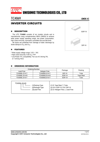
- 1. UNISONIC TECHNOLOGIES CO., LTD TC4069 CMOS IC www.unisonic.com.tw 1 of 5 Copyright © 2011 Unisonic Technologies Co., Ltd QW-R502-635.A INVERTER CIRCUITS „ DESCRIPTION The UTC TC4069 consists of six inverter circuits and is manufactured using complementary MOS (CMOS) to achieve wide power supply operating range, low power consumption, high noise immunity, symmetric controlled rise and fall times. All inputs are protected from damage of static discharge by diode clamps to VDD and VSS. „ FEATURES * Wide supply voltage range: 3.0V ~ 18V. * High noise immunity: 0.45 VDD TYP. * Low Power TTL compatibility: Fan out of 2 driving 74L or 1 driving 74LS. DIP-14 SOP-14 „ ORDERING INFORMATION Ordering Number Lead Free Halogen Free Package Packing TC4069L-D14-T TC4069G-D14-T DIP-14 Tube TC4069L-S14-R TC4069G-S14-R SOP-14 Tape Reel TC4069L-S14-T TC4069G-S14-T SOP-14 Tube
- 2. TC4069 CMOS IC UNISONICTECHNOLOGIESCO.,LTD 2 of 5 www.unisonic.com.tw QW-R502-635.A „ PIN CONFIGURATION 1 2 3 4 5 6 7 14 13 12 11 10 9 VSS 8 VDD „ BLOCK DIAGRAM
- 3. TC4069 CMOS IC UNISONICTECHNOLOGIESCO.,LTD 3 of 5 www.unisonic.com.tw QW-R502-635.A „ ABSOLUTE MAXIMUM RATINGS (Note 2, 3) PARAMETER SYMBOL RATINGS UNIT DC Supply Voltage VDD -0.5 ~ +20 V Input Voltage VIN -0.5 ~ VDD +0.5 V Storage Temperature TS -65 ~ +150 ℃ DIP-14 300 Power Dissipation SOP-14 PD 180 mW Junction Temperature TJ 125 ℃ Operating Temperature TOPR -40 ~ +85 ℃ Storage Temperature TSTG -65 ~ +150 ℃ Notes: 1. Absolute maximum ratings are those values beyond which the device could be permanently damaged. Absolute maximum ratings are stress ratings only and functional device operation is not implied. 2. AC Parameters are guaranteed by DC correlated testing. 3. IOH and IOL are tested one output at a time. „ RECOMMENDED OPERATING CONDITIONS (VSS=0V ) PARAMETER SYMBOL RATINGS UNIT DC Supply Voltage VDD 3 ~ 18 V Input Voltage VIN 0 ~ VDD V Operating Temperature TA -40 ~ 85 ℃ „ DC ELECTRICAL CHARACTERISTICS (TA=25 , ℃ unless otherwise specified.)(Note 2) PARAMETER SYMBOL CONDITIONS MIN TYP MAX UNIT VDD=5V, VIN=VDD or VSS 0.25 VDD=10V, VIN=VDD or VSS 0.5 Quiescent Device Current IDD VDD=15V, VIN=VDD or VSS 1 μA VDD=5V 0 0.05 VDD=10V 0 0.05 Low VOL |IO|<1μA VDD=15V 0 0.05 V VDD=5V 4.95 5 VDD=10V 9.95 10 Output Voltage High VOH |IO|<1μA VDD=15V 14.95 15 V VDD=5V, VO=4.5V 1.0 VDD=10V, VO=9V 2.0 Low VIL |IO|<1μA VDD=15V,VO=13.5V 3.0 V VDD=5V, VO=0.5V 4.0 VDD=10V, VO=1V 8.0 Input Voltage High VIH |IO|<1μA VDD=15V, VO=1.5V 12.0 V VDD=5V, VO=0.4V 0.51 1.2 VDD=10V, VO=0.5V 1.3 3.2 Low IOL VDD=15V, VO=1.5V 3.4 12 mA VDD=5V, VO=4.6V -0.51 -1 VDD=5V, VO=2.5V -2.1 -4 VDD=10V, VO=9.5V -1.3 -2.2 Output Current (Note 3) High IOH VDD=15V, VO=13.5V -3.4 -9 mA VDD=15V, VIN=0V -10 -5 -0.1 Input Current IIN VDD=15V, VIN=15V 10 -5 0.1 μA
- 4. TC4069 CMOS IC UNISONICTECHNOLOGIESCO.,LTD 4 of 5 www.unisonic.com.tw QW-R502-635.A „ AC ELECTRICAL CHARACTERISTICS(Note 1) (TA=25℃, CL=50pF, RL=200kΩ, tr and tf ≤ 20 ns, unless otherwise specified) PARAMETER SYMBOL CONDITIONS MIN TYP MAX UNIT VDD=5V 55 110 VDD=10V 30 60 Propagation Delay Time from Input to Output tPHL or tPLH VDD=15V 25 50 ns VDD=5V 70 200 VDD=10V 35 100 Transition Time tTHL or tTLH VDD=15V 30 80 ns Average Input Capacitance CIN Any Gate 7.5 15 pF Notes: 1. AC Parameters are guaranteed by DC correlated testing. 2. IOH and IOL are tested one output at a time. 3. CPD determines the no load AC power consumption of any CMOS device.
- 5. TC4069 CMOS IC UNISONICTECHNOLOGIESCO.,LTD 5 of 5 www.unisonic.com.tw QW-R502-635.A „ AC TEST CIRCUITS AND SWITCHING TIME WAVEFORMS UTC assumes no responsibility for equipment failures that result from using products at values that exceed, even momentarily, rated values (such as maximum ratings, operating condition ranges, or other parameters) listed in products specifications of any and all UTC products described or contained herein. UTC products are not designed for use in life support appliances, devices or systems where malfunction of these products can be reasonably expected to result in personal injury. Reproduction in whole or in part is prohibited without the prior written consent of the copyright owner. The information presented in this document does not form part of any quotation or contract, is believed to be accurate and reliable and may be changed without notice.