1. CHAPTER 1
INTRODUCTION
Wireless controlled android robot (WI-CAR) is an android robot built in with
ICS which gives user access to remote control it from anywhere in the world. We can
control robot by installing java user client viewer apps and giving our WI-CAR ip
address to it. After giving Ip address to java viewer client like Tight VNC, Ultra
VNC. it remote display robot Android ICS Screen on your Laptop, Pc or smart phone
from which you can give instructions to your WI-CAR and the WI-CAR will do
allotted work for that instructions. WI-CAR will have Inbuilt GPS so that we can
track the location where it is and contains camera to view what’s going on there.
About sensitivity WI-CAR is so sensitive so that you can turn even 20 degrees left
and right and can move 5cms front or back. The speed and video quality depends on
the network for communication you use and it supports many types of networks like
Wi-Fi, 2G, 3G, Edge so on.., but the speed of communication decide its way of
response and minimum preferred is 20Kbps to control it and track the location but if
you want the video then you should choose a higher speed. You can install many
applications in it for free from Google play store like face detection app which help to
find the face that matches with the image that you can send it remotely from
anywhere to WI-CAR using that installed application it can detect the person and send
the response to you. You can connect 128 USB devices externally to WI-CAR and
also 10 sensors on your requirements.
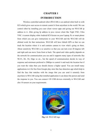
Fig. 1.1: WI-CAR logo
1
2. From its logo we can understand that we control it from any operating system
either it is Windows, Linux or Android it can work for minimum five hours for once
charged. We have a 12 volts and 1 Ampere battery in WI-CAR which is a low power
battery we can increase its battery life by changing the battery. It is easy to install
applications in any type of operating system to control WI-CAR remotely. One of the
excellent that only WI-CAR can do is that we can also give instruction at once before
execution by WI-CAR like go front ten meters turn right twenty degrees then turn left
forty degrees and then right by twenty degrees then go back by ten meters then press
enter you will be surprised to see it is doing it as fully autonomous because it don’t
requires repeated giving of instructions when we are busy and we know what it should
do then we can directly type the commands at once then it will follow the instructions
sequentially and there is a chance to save the command sequence by giving a name to
it.
2
3. CHAPTER 2
AVR
The ATmega16 is a low-power CMOS 8-bit microcontroller based on the
AVR enhanced RISC architecture. By executing powerful instructions in a single
clock cycle, the ATmega16 achieves throughputs approaching 1 MIPS per MHz
allowing the system designed to optimize power consumption versus processing
speed.
Fig. 2.1: Block Diagram
3
4. The AVR core combines a rich instruction set with 32 general purpose
working registers. All the 32 registers are directly connected to the Arithmetic Logic
Unit (ALU), allowing two independent registers to be accessed in one single
instruction executed in one clock cycle. The resulting architecture is more code
efficient while achieving throughputs up to ten times faster than conventional CISC
microcontrollers. The ATmega16 provides the following features: 16K bytes of In-
System Programmable Flash Program memory with Read-While-Write capabilities,
512 bytes EEPROM, 1K byte SRAM, 32 general purpose I/O lines, 32 general
purpose working registers, a JTAG interface for Boundary scan, On-chip Debugging
support and programming, three flexible Timer/Counters with compare modes,
Internal and External Interrupts, a serial programmable USART, a byte oriented Two-
wire Serial Interface, an 8-channel, 10-bit ADC with optional differential input stage
with programmable gain (TQFP package only), a programmable Watchdog Timer
with Internal Oscillator, an SPI serial port, and six software selectable power saving
modes. The Idle mode stops the CPU while allowing the USART, Two-wire interface,
A/D Converter, SRAM, Timer/Counters, SPI port, and interrupt system to continue
functioning.
The Power-down mode saves the register contents but freezes the Oscillator,
disabling all other chip functions until the next External Interrupt or Hardware Reset.
In Power-save mode, the Asynchronous Timer continues to run, allowing the user to
maintain a timer base while the rest of the device is sleeping. The ADC Noise
Reduction mode stops the CPU and all I/O modules except Asynchronous Timer and
ADC, to minimize switching noise during ADC conversions. In Standby mode, the
crystal/resonator Oscillator is running while the rest of the device is sleeping. This
allows very fast start-up combined with low-power consumption. In Extended
Standby mode, both the main Oscillator and the Asynchronous Timer continue to run.
The device is manufactured using Atmel’s high density nonvolatile memory
technology. The Onchip ISP Flash allows the program memory to be reprogrammed
in-system through an SPI serial interface, by a conventional nonvolatile memory
programmer, or by an On-chip Boot program running on the AVR core. The boot
program can use any interface to download the application program in the Application
Flash memory.
Software in the Boot Flash section will continue to run while the Application
Flash section is updated, providing true Read-While-Write operation. By combining
4
5. an 8-bit RISC CPU with In-System Self-Programmable Flash on a monolithic chip,
the Atmel ATmega16 is a powerful microcontroller that provides a highly-flexible
and cost-effective solution to many embedded control applications. The ATmega16
AVR is supported with a full suite of program and system development tools
including: C compilers, macro assemblers, program debugger/simulators, in-circuit
emulators, and evaluation kits.
AVR CPU Core
This section discusses the AVR core architecture in general. The main function of the
CPU core is to ensure correct program execution. The CPU must therefore be able to
access memories, perform calculations, control peripherals, and handle interrupts.
2.1 ARCHITECTURAL OVERVIEW
Fig. 2.2: Block Diagram of the AVR MCU Architecture
In order to maximize performance and parallelism, the AVR uses a Harvard
architecture – with separate memories and buses for program and data. Instructions in
the program memory are executed with a single level pipelining. While one
instruction is being executed, the next instruction is pre-fetched from the program
memory. This concept enables instructions to be executed in every clock cycle. The
program memory is In-System Reprogrammable Flash memory. The fast-access
5
6. Register File contains 32 x 8-bit general purpose working registers with a single clock
cycle access time. This allows single-cycle Arithmetic Logic Unit (ALU) operation.
In a typical ALU operation, two operands are output from the Register File, the
operation is executed, and the result is stored back in the Register File – in one clock
cycle. Six of the 32 registers can be used as three 16-bit indirect addresses register
pointers for Data Space addressing – enabling efficient address calculations. One of
these address pointers can also be used as an address pointer for look up tables in
Flash Program memory. These added function registers are the 16-bit X-, Y-, and Z-
register, described later in this section.
The ALU supports arithmetic and logic operations between registers or
between a constant and a register. Single register operations can also be executed in
the ALU. After an arithmetic operation, the Status Register is updated to reflect
information about the result of the operation. Program flow is provided by conditional
and unconditional jump and call instructions, able to directly address the whole
address space. Most AVR instructions have a single 16-bit word format. Every
program memory address contains a 16- or 32-bit instruction. Program Flash memory
space is divided in two sections, the Boot program section and the Application
Program section. Both sections have dedicated Lock bits for write and read/write
protection. The SPM instruction that writes into the Application Flash memory
section must reside in the Boot Program section. During interrupts and subroutine
calls, the return address Program Counter (PC) is stored on the Stack. The Stack is
effectively allocated in the general data SRAM, and consequently the Stack size is
only limited by the total SRAM size and the usage of the SRAM.
All user programs must initialize the SP in the reset routine (before
subroutines or interrupts are executed). The Stack Pointer SP is read/write accessible
in the I/O space. The data SRAM can easily be accessed through the five different
addressing modes supported in the AVR architecture. The memory spaces in the AVR
architecture are all linear and regular memory maps. A flexible interrupt module has
its control registers in the I/O space with an additional global interrupt enable bit in
the Status Register. All interrupts have a separate interrupt vector in the interrupt
vector table. The interrupts have priority in accordance with their interrupt vector
position. The lower the interrupt vector address, the higher the priority. The I/O
memory space contains 64 addresses for CPU peripheral functions as Control
6
7. Registers, SPI, and other I/O functions. The I/O Memory can be accessed directly, or
as the Data Space locations following those of the Register File, $20 - $5F.
ALU – Arithmetic Logic Unit
The high-performance AVR ALU operates in direct connection with all the 32
general purpose working registers. Within a single clock cycle, arithmetic operations
between general purpose registers or between a register and an immediate are
executed. The ALU operations are divided into three main categories – arithmetic,
logical, and bit-functions. Some implementations of the architecture also provide a
powerful multiplier supporting both signed/unsigned multiplication and fractional
format. See the “Instruction Set” section for a detailed description.
Status Register
The Status Register contains information about the result of the most recently
executed arithmetic instruction. This information can be used for altering program
flow in order to perform conditional operations. Note that the Status Register is
updated after all ALU operations, as specified in the Instruction Set Reference. This
will in many cases remove the need for using the dedicated compare instructions,
resulting in faster and more compact code. The Status Register is not automatically
stored when entering an interrupt routine and restored when returning from an
interrupt. This must be handled by software. The AVR Status Register – SREG – is
defined as
The Global Interrupt Enable bit must be set for the interrupts to be enabled.
The individual interrupt enable control is then performed in separate control registers.
If the Global Interrupt Enable Register is cleared, none of the interrupts are enabled
independent of the individual interrupt enable settings. The I-bit is cleared by
hardware after an interrupt has occurred, and is set by the RETI instruction to enable
subsequent interrupts. The I-bit can also be set and cleared by the application with the
SEI and CLI instructions, as described in the instruction set reference.
7
8. Bit 6 – T: Bit Copy Storage
The Bit Copy instructions BLD (Bit LoaD) and BST (Bit STore) use the T-bit as
source or destination for the operated bit. A bit from a register in the Register File can
be copied into T by the BST instruction, and a bit in T can be copied into a bit in a
register in the Register File by the BLD instruction.
Bit 5 – H: Half Carry Flag
The Half Carry Flag H indicates a Half Carry in some arithmetic operations.
Half Carry is useful in BCD arithmetic. See the “Instruction Set Description” for
detailed information.
Bit 4 – S: Sign Bit, S = N ⊕V
The S-bit is always an exclusive or between the Negative Flag N and the
Two’s Complement Overflow Flag V. See the “Instruction Set Description” for
detailed information.
Bit 3 – V: Two’s Complement Overflow Flag
The Two’s Complement Overflow Flag V supports two’s complement
arithmetic’s. See the “Instruction Set Description” for detailed information.
Bit 2 – N: Negative Flag
The Negative Flag N indicates a negative result in an arithmetic or logic
operation. See the “Instruction Set Description” for detailed information.
Bit 1 – Z: Zero Flag
The Zero Flag Z indicates a zero result in an arithmetic or logic operation. See
the “Instruction Set Description” for detailed information.
Bit 0 – C: Carry Flag
The Carry Flag C indicates a carry in an arithmetic or logic operation. See the
“Instruction Set Description” for detailed information.
General Purpose Register File
The Register File is optimized for the AVR Enhanced RISC instruction set. In
order to achieve the required performance and flexibility, the following input/output
schemes are supported by the Register File
• One 8-bit output operand and one 8-bit result input
• Two 8-bit output operands and one 8-bit result input
• Two 8-bit output operands and one 16-bit result input
• One 16-bit output operand and one 16-bit result input
8
9. Fig. 2.3: AVR CPU General Purpose Working Registers
Most of the instructions operating on the Register File have direct access to all
registers, and most of them are single cycle instructions. As shown in fig 2.3 each
register is also assigned a data memory address, mapping them directly into the first
32 locations of the user Data Space. Although not being physically implemented as
SRAM locations, this memory organization provides great flexibility in access of the
registers, as the X-, Y-, and Z-pointer Registers can be set to index any register in the
file.
The X-register, Y-register and Z-register
The registers R26.R31 have some added functions to their general purpose
usage. These registers are 16-bit address pointers for indirect addressing of the Data
Space. The three indirect address registers X, Y, and Z are defined as described in
fig.2.4.
9
10. Fig. 2.4: The X-, Y-, and Z-registers
2.2 STACK POINTER
The Stack is mainly used for storing temporary data, for storing local variables
and for storing return addresses after interrupts and subroutine calls. The Stack
Pointer Register always points to the top of the Stack. Note that the Stack is
implemented as growing from higher memory locations to lower memory locations.
This implies that a Stack PUSH command decreases the Stack Pointer.
If software reads the Program Counter from the Stack after a call or an
interrupt, unused bits (15:13) should be masked out. The Stack Pointer points to the
data SRAM Stack area where the Subroutine and Interrupt Stacks are located.
This Stack space in the data SRAM must be defined by the program before
any subroutine calls are executed or interrupts are enabled. The Stack Pointer must be
set to point above $60. The Stack Pointer is decremented by one when data is pushed
onto the Stack with the PUSH instruction, and it is decremented by two when the
return address is pushed onto the Stack with subroutine call or interrupt.
The Stack Pointer is incremented by one when data is popped from the Stack
with the POP instruction, and it is incremented by two when data is popped from the
Stack with return from subroutine RET or return from interrupt RETI. The AVR
Stack Pointer is implemented as two 8-bit registers in the I/O space. The number of
bits actually used is implementation dependent. Note that the data space in some
implementations of the AVR architecture is so small that only SPL is needed. In this
case, the SPH Register will not be present.
10
11. Instruction Execution Timing
This section describes the general access timing concepts for instruction
execution. The AVR CPU is driven by the CPU clock CPU, directly generated from
the selected clock source for the chip. No internal clock division is used. Fig.2.5
shows the parallel instruction fetches and instruction executions enabled by the
Harvard architecture and the fast-access Register File concept. This is the basic
pipelining concept to obtain up to 1 MIPS per MHz with the corresponding unique
results for functions per cost, functions per clocks, and functions per power-unit.
Fig 2.5: The Parallel Instruction Fetches and Instruction Executions
Fig.2.6 shows the internal timing concept for the Register File. In a single
clock cycle an ALU operation using two register operands is executed, and the result
is stored back to the destination register.
Fig.2.6: Single Cycle ALU Operation
11
12. Reset and Interrupt Handling
The AVR provides several different interrupt sources. These interrupts and the
separate reset vector each have a separate program vector in the program memory
space. All interrupts are assigned individual enable bits which must be written logic
one together with the Global Interrupt Enable bit in the Status Register in order to
enable the interrupt. Depending on the Program Counter value, interrupts may be
automatically disabled when Boot Lock bits BLB02 or BLB12 are programmed. This
feature improves software security. See the section “Memory Programming” on page
259 for details. The lowest addresses in the program memory space are by default
defined as the Reset and Interrupt Vectors. The complete list of vectors is shown in
“Interrupts” on page 45. The list also determines the priority levels of the different
interrupts. The lower the address the higher is the priority level. RESET has the
highest priority, and next is INT0 – the External Interrupt Request 0.
The Interrupt Vectors can be moved to the start of the Boot Flash section by
setting the IVSEL bit in the General Interrupt Control Register (GICR). Refer to
“Interrupts” on page 45 for more information. The Reset Vector can also be moved to
the start of the boot Flash section by programming the BOOTRST Fuse, see “Boot
Loader Support – Read-While-Write Self- Programming”. When an interrupt occurs,
the Global Interrupt Enable I-bit is cleared and all interrupts are disabled. The user
software can write logic one to the I-bit to enable nested interrupts. All enabled
interrupts can then interrupt the current interrupt routine. The I-bit is automatically set
when a Return from Interrupt instruction – RETI – is executed. There are basically
two types of interrupts. The first type is triggered by an event that sets the Interrupt
Flag. For these interrupts, the Program Counter is vectored to the actual Interrupt
Vector in order to execute the interrupt handling routine, and hardware clears the
corresponding Interrupt Flag. Interrupt Flags can also be cleared by writing a logic
one to the flag bit position(s) to be cleared.
If an interrupt condition occurs while the corresponding interrupt enable bit is
cleared, the Interrupt Flag will be set and remembered until the interrupt is enabled, or
the flag is cleared by software. Similarly, if one or more interrupt conditions occur
while the Global Interrupt Enable bit is cleared, the corresponding Interrupt Flag(s)
will be set and remembered until the global interrupt enable bit is set, and will then be
executed by order of priority. The second type of interrupts will trigger as long as the
interrupt condition is present. These interrupts do not necessarily have Interrupt Flags.
12
13. If the interrupt condition disappears before the interrupt is enabled, the interrupt will
not be triggered. When the AVR exits from an interrupt, it will always return to the
main program and execute one more instruction before any pending interrupt is
served. Note that the Status Register is not automatically stored when entering an
interrupt routine, nor restored when returning from an interrupt routine. This must be
handled by software. When using the CLI instruction to disable interrupts, the
interrupts will be immediately disabled. No interrupt will be executed after the CLI
instruction, even if it occurs simultaneously with the CLI instruction. The following
example shows how this can be used to avoid interrupts during the timed EEPROM
write sequence.
Interrupt Response Time
The interrupt execution response for all the enabled AVR interrupts is four
clock cycles minimum. After four clock cycles the program vector address for the
actual interrupt handling routine is executed. During this four clock cycle period, the
Program Counter is pushed onto the Stack. The vector is normally a jump to the
interrupt routine, and this jump takes three clock cycles. If an interrupt occurs during
execution of a multi-cycle instruction, this instruction is completed before the
interrupt is served. If an interrupt occurs when the MCU is in sleep mode, the
interrupt execution response time is increased by four clock cycles. This increase
comes in addition to the start-up time from the selected sleep mode. A return from an
interrupt handling routine takes four clock cycles. During these four clock cycles, the
Program Counter (two bytes) is popped back from the Stack, the Stack Pointer is
incremented by two, and the I-bit in SREG is set.
2.3 AVR ATMEGA16 MEMORIES
This section describes the different memories in the ATmega16. The AVR
architecture has two main memory spaces, the Data Memory and the Program
Memory space. In addition, the ATmega16 features an EEPROM Memory for data
storage. All three memory spaces are linear and regular.
In-System Reprogrammable Flash Program Memory
The ATmega16 contains 16K bytes On-chip In-System Reprogrammable
Flash memory for program storage. Since all AVR instructions are 16 or 32 bits wide,
the Flash is organized as 8K x 16. For software security, the Flash Program memory
space is divided into two sections, Boot Program section and Application Program
13
14. section. The Flash memory has an endurance of at least 10,000 write/erase cycles. The
ATmega16 Program Counter (PC) is 13 bits wide, thus addressing the 8K program
memory locations. The operation of Boot Program section and associated Boot Lock
bits for software protection are described in detail in “Boot Loader Support – Read-
While-Write Self-Programming” on page 246. “Memory Programming” on page 259
contains a detailed description on Flash data serial downloading using the SPI pins or
the JTAG interface. Constant tables can be allocated within the entire program
memory address space (see the LPM – Load Program Memory Instruction
Description). Timing diagrams for instruction fetch and execution are presented in
“Instruction Execution Timing”
Fig. 2.7: Program Memory Map
2.4 SRAM DATA MEMORY
Fig.2.8 shows how the ATmega16 SRAM Memory is organized. The lower
1120 Data Memory locations address the Register File, the I/O Memory, and the
internal data SRAM. The first 96 locations address the Register File and I/O Memory,
and the next 1024 locations address the internal data SRAM. The five different
addressing modes for the data memory cover: Direct, Indirect with Displacement,
14
15. Indirect, Indirect with Pre-decrement, and Indirect with Post-increment. In the
Register File, registers R26 to R31 feature the indirect addressing pointer registers.
The direct addressing reaches the entire data space.
The Indirect with Displacement mode reaches 63 address locations from the
base address given by the Y- or Z-register. When using register indirect addressing
modes with automatic pre-decrement and post-increment, the address registers X, Y,
and Z are decremented or incremented. The 32 general purpose working registers, 64
I/O Registers, and the 1024 bytes of internal data SRAM in the ATmega16 are all
accessible through all these addressing modes. The Register File is described in
“General Purpose Register File”
Fig 2.8: Data Memory Map
Data Memory Access Times
This section describes the general access timing concepts for internal memory access.
The internal data SRAM access is performed in two clock CPU cycles as described in
Fig.2.9
15
16. Fig 2.9: On-chip Data SRAM Access Cycles
EEPROM Data Memory
The ATmega16 contains 512 bytes of data EEPROM memory. It is organized
as a separate data space, in which single bytes can be read and written. The EEPROM
has an endurance of at least 100,000 write/erase cycles. The access between the
EEPROM and the CPU is described in the following, specifying the EEPROM
Address Registers, the EEPROM Data Register, and the EEPROM Control Register.
For a detailed description of SPI, JTAG and Parallel data downloading to the
EEPROM.
EEPROM Read/Write Access
The EEPROM Access Registers are accessible in the I/O space. The write
access time for the EEPROM is given in Table 1. A self-timing function, however,
lets the user software detect when the next byte can be written. If the user code
contains instructions that write the EEPROM, some precautions must be taken. In
heavily filtered power supplies, VCC is likely to rise or fall slowly on Power-
up/down. This causes the device for some period of time to run at a voltage lower
than specified as minimum for the clock frequency used. See “Preventing EEPROM
Corruption” on page 22 for details on how to avoid problems in these situations. In
order to prevent unintentional EEPROM writes, a specific write procedure must be
followed. Refer to the description of the EEPROM Control Register for details on
this. When the EEPROM is read, the CPU is halted for four clock cycles before the
16
17. next instruction is executed. When the EEPROM is written, the CPU is halted for two
clock cycles before the next instruction is executed.
The EEPROM Address Register – EEARH and EEARL
The EEPROM Address Registers – EEARH and EEARL – specify the
EEPROM address in the 512 bytes EEPROM space. The EEPROM data bytes are
addressed linearly between 0 and 511. The initial value of EEAR is undefined. A
proper value must be written before the EEPROM may be accessed.
The EEPROM Data Register – EEDR
For the EEPROM write operation, the EEDR Register contains the data to be
written to the EEPROM in the address given by the EEAR Register. For the
EEPROM read operation, the EEDR contains the data read out from the EEPROM at
the address given by EEAR.
The EEPROM Control Register – EECR
These bits are reserved bits in the ATmega16 and will always read as zero.
Writing EERIE to one enables the EEPROM Ready Interrupt if the I bit in SREG is
17
18. set. Writing EERIE to zero disables the interrupt. The EEPROM Ready interrupt
generates a constant interrupt when EEWE is cleared. The EEMWE bit determines
whether setting EEWE to one causes the EEPROM to be written. When EEMWE is
set, setting EEWE within four clock cycles will write data to the EEPROM at the
selected address If EEMWE is zero, setting EEWE will have no effect.
When EEMWE has been written to one by software, hardware clears the bit to
zero after four clock cycles. See the description of the EEWE bit for an EEPROM
write procedure. The EEPROM Write Enable Signal EEWE is the write strobe to the
EEPROM. When address and data are correctly set up, the EEWE bit must be written
to one to write the value into the EEPROM. The EEMWE bit must be written to one
before a logical one is written to EEWE, otherwise no EEPROM write takes place.
The following procedure should be followed when writing the EEPROM (the order of
steps 3 and 4 is not essential)
1. Wait until EEWE becomes zero.
2. Wait until SPMEN in SPMCR becomes zero.
3. Write new EEPROM address to EEAR (optional).
4. Write new EEPROM data to EEDR (optional).
5. Write a logical one to the EEMWE bit while writing a zero to EEWE in
EECR.
6. Within four clock cycles after setting EEMWE, write a logical one to EEWE.
The EEPROM cannot be programmed during a CPU write to the Flash
memory. The software must check that the Flash programming is completed before
initiating a new EEPROM write. Step 2 is only relevant if the software contains a
Boot Loader allowing the CPU to program the Flash. If the Flash is never being
updated by the CPU, step 2 can be omitted. See “Boot Loader Support – Read-While-
Write Self-Programming” on page 246 for details about boot programming. An
interrupt between step 5 and step 6 will make the write cycle fail, since the EEPROM
Master Write Enable will time-out.
If an interrupt routine accessing the EEPROM is interrupting another
EEPROM Access, the EEAR or EEDR reGister will be modified, causing the
interrupted EEPROM Access to fail. It is recommended to have the Global Interrupt
Flag cleared during all the steps to avoid these problems. When the write access time
has elapsed, the EEWE bit is cleared by hardware. The user software can poll this bit
18
19. and wait for a zero before writing the next byte. When EEWE has been set, the CPU
is halted for two cycles before the next instruction is executed.
The EEPROM Read Enable Signal – EERE – is the read strobe to the
EEPROM. When the correct address is set up in the EEAR Register, the EERE bit
must be written to a logic one to trigger the EEPROM read. The EEPROM read
access takes one instruction, and the requested data is available immediately. When
the EEPROM is read, the CPU is halted for four cycles before the next instruction is
executed. The user should poll the EEWE bit before starting the read operation. If a
write operation is in progress, it is neither possible to read the EEPROM, nor to
change the EEAR Register. The calibrated Oscillator is used to time the EEPROM
accesses. Table 1 lists the typical programming time for EEPROM access from the
CPU.
Minimizing Power Consumption
There are several issues to consider when trying to minimizing the power
consumption in an AVR controlled system. In general, sleep modes should be used as
much as possible, and the sleep mode should be selected so that as few as possible of
the device’s functions are operating. All functions not needed should be disabled. In
particular, the following modules may need special consideration when trying to
achieve the lowest possible power consumption.
Analog to Digital Converter
If enabled, the ADC will be enabled in all sleep modes. To save power, the
ADC should be disabled before entering any sleep mode. When the ADC is turned off
and on again, the next conversion will be an extended conversion. Refer to “Analog to
Digital Converter” on page 204 for details on ADC operation.
Analog Comparator
When entering idle mode, the Analog Comparator should be disabled if not
used. When entering ADC Noise Reduction mode, the Analog Comparator should be
disabled. In the other sleep modes, the Analog Comparator is automatically disabled.
However, if the Analog Comparator is set up to use the Internal Voltage Reference as
input, the Analog Comparator should be disabled in all sleep modes. Otherwise, the
19
20. Internal Voltage Reference will be enabled, independent of sleep mode. Refer to
“Analog Comparator” on page 201 for details on how to configure the Analog
Comparator.
Brown-out Detector
If the Brown-out Detector is not needed in the application, this module should
be turned off. If the Brown-out Detector is enabled by the BODEN Fuse, it will be
enabled in all sleep modes, and hence, always consume power. In the deeper sleep
modes, this will contribute significantly to the total current consumption. Refer to
“Brown-out Detection” on page 40 for details on how to configure the Brown-out
Detector.
Internal Voltage Reference
The Internal Voltage Reference will be enabled when needed by the Brown-
out Detector, the Analog Comparator or the ADC. If these modules are disabled as
described in the sections above, the internal voltage reference will be disabled and it
will not be consuming power. When turned on again, the user must allow the
reference to start up before the output is used. If the reference is kept on in sleep
mode, the output can be used immediately. Refer to “Internal Voltage Reference”.
Watchdog Timer
If the Watchdog Timer is not needed in the application, this module should be
turned off. If the Watchdog Timer is enabled, it will be enabled in all sleep modes,
and hence, always consume power. In the deeper sleep modes, this will contribute
significantly to the total current consumption. Port Pins When entering a sleep mode,
all port pins should be configured to use minimum power. The most important thing is
then to ensure that no pins drive resistive loads. In sleep modes where the both the I/O
clock (clock I/O) and the ADC clock (clock ADC) are stopped, the input buffers of
the device will be disabled.
This ensures that no power is consumed by the input logic when not needed.
In some cases, the input logic is needed for detecting wake-up conditions, and it will
then be enabled. Refer to the section “Digital Input Enable and Sleep Modes” details
on which pins are enabled. If the input buffer is enabled and the input signal is left
20
21. floating or have an analog signal level close to VCC/2, the input buffer will use
excessive power.
JTAG Interface and On-chip Debug System
If the On-chip debug system is enabled by the OCDEN Fuse and the chip enter
Power down or Power save sleep mode, the main clock source remains enabled. In
these sleep modes, this will contribute significantly to the total current consumption.
There are three alternative ways to avoid this
• Disable OCDEN Fuse.
• Disable JTAGEN Fuse.
• Write one to the JTD bit in MCUCSR.
The TDO pin is left floating when the JTAG interface is enabled while the
JTAG TAP controller is not shifting data. If the hardware connected to the TDO pin
does not pull up the logic level, power consumption will increase. Note that the TDI
pin for the next device in the scan chain contains a pull-up that avoids this problem.
Writing the JTD bit in the MCUCSR register to one or leaving the JTAG fuse un
programmed disables the JTAG interface.
21
22. CHAPTER 3
WINDOWS XP
An operating system produced by Microsoft for use on personal computers,
including home and business desktops, laptops and media centers. First released to
computer manufacturers on August 24, 2001, it is the second most popular version
of Windows, based on installed user base. The name "XP" is short for
"experience", highlighting the enhanced user experience.
Windows XP, the successor to Windows 2000 and Windows ME, was the first
consumer-oriented operating system produced by Microsoft to be built on the
Windows NT kernel. Windows XP was released worldwide for retail sale on October
25, 2001, and over 400 million copies were in use in January 2006. It was succeeded
by Windows Vista in January 2007. Direct OEM and retail sales of Windows XP
ceased on June 30, 2008. Microsoft continued to sell Windows XP through their
System Builders (smaller OEMs who sell assembled computers) program until
January 31, 2009. On April 10, 2012, Microsoft reaffirmed that extended support for
Windows XP and Office 2003 would end on April 8, 2014 and suggested that
administrators begin preparing to migrate to a newer OS.
The NT-based versions of Windows, which are programmed in C, C++, and
assembly, are known for their improved stability and efficiency over the 9xversions
of Microsoft Windows. Windows XP presented a significantly redesigned graphical
user interface, a change Microsoft promoted as more user-friendly than previous
versions of Windows. In an attempt to further ameliorate the "DLL hell" that plagued
the past versions of Windows, improved side-by-side assembly technology in
Windows XP allows side-by-side installation, registration and servicing of multiple
versions of globally shared software components in full isolation. It is also the first
version of Windows to use product activation to combat illegal copying.
During Windows XP's development, the project was codenamed "Whistler",
after Whistler, British Columbia, as many Microsoft employees skied at the Whistler-
Blackcomb ski resort.
According to web analytics data generated by Net Applications, Windows
XP was the most widely used operating system until August 2012, when Windows
7overtook it. As of February 2013, Windows XP market share is at 38.99%, having
22
23. decreased almost every month since at least November 2007, the first month for
which statistics are publicly available from Net Applications.
User Interface
Windows XP featured a new task-based GUI (Graphical user interface).
The Start menu and taskbar were updated and many visual effects were added,
including:
• A translucent blue selection rectangle in Windows Explorer
• Drop shadows for icon labels on the desktop
• Task-based sidebars in Explorer windows ("common tasks")
• The ability to group the taskbar buttons of the windows of one application into
one button, with a popup menu listing the window titles
• The ability to lock the taskbar to prevent accidental changes (Windows 2000
with Internet Explorer 6 installed had the ability to lock Windows Explorer
and Internet Explorer toolbars, but not the taskbar)
• The highlighting of recently added programs on the Start menu
• Shadows under menus (Windows 2000 had shadows under mouse pointers,
but not menus)
Windows XP analyzes the performance impact of visual effects and uses this
to determine whether to enable them, so as to prevent the new functionality from
consuming excessive additional processing overhead. Users can further customize
these settings. Some effects, such as alpha compositing (transparency and fading), are
handled entirely by many newer video cards. However, if the video card is not
capable of hardware alpha blending, performance can be substantially degraded, and
Microsoft recommends the feature should be turned off manually.[23]
Windows XP
added the ability for Windows to use "Visual Styles" to change the appearance of the
user interface.
However, visual styles must be cryptographically signed by Microsoft to
run. Luna is the name of the new visual style that is provided with Windows XP, and
is enabled by default for machines with more than 64 MB of RAM. Luna refers only
to one particular visual style, not to all of the new user interface features of Windows
XP as a whole. Some users "patch" the uxtheme.dll file that restricts the ability to use
visual styles, created by the general public or the user, on Windows XP.
23
24. In addition to the included Windows XP themes, there is one previously
unreleased theme with a dark blue taskbar and window bars similar to Windows Vista
titled "Royale Noir" available as unofficial download.[25]
Microsoft officially released
a modified version of this theme as the "Zune" theme, to celebrate the launch of its
Zune portable media player in November 2006. The differences are only visual with a
new glassy look along with a black taskbar instead of dark blue and an orange start
button instead of green.[26]
Additionally, the Media Center "Royale" theme, which was
included in the Media Center editions, is also available to download for use on all
Windows XP editions.[27]
The default wallpaper, Bliss, is a photo of a landscape in the Napa
Valley outside Napa, California,[28]
with rolling green hills and a blue sky
with stratocumulus and cirrus clouds.
The "classic" interface from Windows 9x and 2000 can be used instead if preferred.
Several third party utilities exist that provide hundreds of different visual styles.
• Improved imaging features such as Windows Picture and Fax Viewer,
improved image handling and thumbnail caching in Explorer
• A number of kernel enhancements and power management improvements
• Faster start-up, (due to improved Pre fetch functions) logon,
logoff, hibernation and application launch sequences.
• The ability to discard a newer device driver in favor of the previous one
(known as driver rollback) should a driver upgrade not produce desirable
results.
• Numerous improvements to increase the system reliability such as
improved System Restore, Recovery, Windows and driver reliability.
• A new, arguably more user-friendly interface, including the framework for
developing themes for the desktop environment and richer icons with alpha
transparency
• Hardware support improvements such as USB 2.0, FireWire 800, Windows
Image Acquisition, Media Transfer Protocol, and Dual View for multi-
monitors and audio improvements.
• Fast user switching, which allows users to save the current state and open
applications of their desktop and allows another user to log on without losing
that information
24
25. • The Clear Type font rendering mechanism, which is designed to improve text
readability on liquid crystal display (LCD) and similar monitors, especially
laptops.
• Remote Assistance and Remote Desktop features, which allow users to
connect to a computer running Windows XP from across a network or
the Internet and access their applications, files, printers, and devices or request
help.
• New networking features including Windows Firewall, Internet Connection
Sharing integration with UPnP, NAT traversal APIs, Quality of Service
features, IPv6 and Teredo tunneling, Background Intelligent Transfer Service,
extended fax features, network bridging, peer to peer networking, support for
most DSL modems, IEEE 802.11 (Wi-Fi) connections with auto
configuration and roaming, TAPI 3.1, Bluetooth and networking
over FireWire.
• New security features such as Software Restriction Policies, Credential
Manager, Encrypting File System improvements, improved certificate
services, smart card and PKI support. Windows XP SP2 introduced Data
Execution Prevention, Center and Attachment Manager.
• Side-by-side assemblies and registration-free COM
• Improved media features in Windows Media format runtime, Windows Media
Player, Windows Movie Maker, TV/video capture and playback
technologies, Windows Media Encoder and introduction of Windows Media
Center
• General improvements to international support such as more locales,
languages and scripts, MUI support in Terminal Services, improved IMEs and
National Language Support, Text Services Framework
• Handwriting recognition, speech recognition and digital ink support accessible
through the Tablet PC Input Panel (TIP) in Windows XP Tablet PC Edition
• Numerous improvements to system administration tools such as Windows
Installer, Windows Script Host, Defragmenter, Windows, Group
Policy, CHKDSK, NTBackup, Microsoft Management Console, Shadow
Copy, Registry Editor, Sysprep and WMI
• Improved application compatibility and shims compared to Windows 2000
25
26. • Updated accessories and games.
• Improvements to IntelliMirror features such as Offline Files, Roaming user
profiles and Folder redirection.
Users in British schools observed the improved ease of use and advanced
capabilities – comparing the former to RISC OS and Mac OS, and the latter to Unix.
3.1 EDITIONS
Fig. 3.1: Diagram Representing the Main Editions of Windows XP
It is based on the category of the edition (grey) and codebase (blak arrow).
The two major editions are Windows XP Home Edition, designed for home users, and
Windows XP Professional, designed for business and power users. XP Professional
contains advanced features that the average home user would not use. However, these
features are not necessarily missing from XP Home. They are simply disabled, but are
there and can become functional. These releases were made available at retail outlets
that sell computer software, and were preinstalled on computers sold by major
computer manufacturers. A third edition, called Windows XP Media Center Edition,
was introduced in 2002 and was updated every year until 2006 to incorporate new
digital media, broadcast television and Media Center Extender capabilities. Unlike the
Home and Professional edition, it was never made available for retail purchase, and
was typically either sold through OEM channels, or was preinstalled on computers
that were typically marketed as "media center PCs".
Two different 64-bit editions were made available. One, designed specifically
for Itanium-based workstations, was introduced in 2001 at around the same time as
26
27. the Home and Professional editions, but was discontinued a few years later when
vendors of Itanium hardware stopped selling workstation-class machines due to low
sales. The other, called Windows XP Professional x64 Edition, supports the x86-64
extension. x86-64 was implemented first by AMD as "AMD64", found in
AMD's Opteron and Athlon 64 chips, and later implemented by Intel as "Intel 64"
(formerly known as IA-32e and EM64T), found in some of Intel's Pentium 4 and later
chips.
Windows XP Tablet PC Edition was produced for a class of specially designed
notebook/laptop computers called tablet PCs. It is compatible with a pen-sensitive
screen, supporting handwritten notes and portrait-oriented screens.
Fig.3.2: Internet Explorer 6 running in Windows XP Tablet PC Edition 2004
Microsoft also released Windows XP Embedded, an edition for specific
consumer electronics, set-top boxes, kiosks/ATMs, medical devices, arcade video
games, point-of-sale terminals, and Voice over Internet Protocol (VoIP) components.
In July 2006, Microsoft released Windows Fundamentals for Legacy PCs, a thin
client version of Windows XP Embedded which targets older machines (as early as
the original Pentium). It is only available to Software Assurance customers. It is
intended for corporate customers who may wish to upgrade to Windows XP so they
can take advantage of its security and management capabilities, but cannot afford to
purchase new hardware.
3.2 EDITIONS FOR SPECIFIC MARKETS
27
28. Windows XP Starter Edition is a lower-cost edition of Windows XP available
in Thailand, Indonesia, Russia, India, Colombia, Brazil, Argentina, Peru, Bolivia,
Chile, Mexico, Ecuador, Uruguay, Pakistan and Venezuela. It is similar to Windows
XP Home, but is limited to low-end hardware, can only run three programs at a time,
and has some other features either removed or disabled by default. Each country's
edition is also customized for that country, including desktop backgrounds of popular
locations, localized help features for those who may not speak English, and other
default settings designed for easier use than typical Windows XP installations. The
Malaysian version, for example, contains a desktop background of the Kuala
Lumpur skyline.
In March 2004, the European Commission fined Microsoft €497 million
(US$603 million) and ordered the company to provide a version of Windows
without Windows Media Player. The Commission concluded that Microsoft
"broke European Union competition law by leveraging its near monopoly in the
market for PC operating systems onto the markets for work group server operating
systems and for media players". After unsuccessful appeals in 2004 and 2005,
Microsoft reached an agreement with the Commission where it would release a court-
compliant version, Windows XP Edition N. This version does not include the
company's Windows Media Player but instead encourages users to pick and download
their own media player. Microsoft wanted to call this version Reduced Media Edition,
but EU regulators objected and suggested the Edition N name, with the N signifying
"not with Media Player" for both Home and Professional editions of Windows XP.
Because it is sold at the same price as the version with Windows Media Player
included, Dell, Hewlett, Lenovo and Fujitsu Siemens have chosen not to stock the
product. However, Dell did offer the operating system for a short time. Consumer
interest has been low, with roughly 1,500 units shipped to OEMs, and no reported
sales to consumers.
In December 2005, the Korean Fair Trade Commission ordered Microsoft to
make available editions of Windows XP and Windows Server 2003 that do not
contain Windows Media Player or Windows Messenger. Like the European
Commission decision, this decision was based on the grounds that Microsoft had
abused its dominant position in the market to push other products onto consumers.
Unlike that decision, however, Microsoft was also forced to withdraw the non-
compliant versions of Windows from the South Korean market. This decision resulted
28
29. in Microsoft's releasing "K" and "KN" variants of the Home and Professional editions
in August 2006.
That same year, Microsoft also released two additional editions of Windows
XP Home Edition directed towards subscription-based and pay-as-you-go pricing
models. These editions, released as part of Microsoft's FlexGo initiative, are used in
conjunction with a hardware component to enforce time limitations on the usage of
Windows. Its target market is emerging economies such as Brazil and Vietnam.
Languages
Windows XP was available in many languages. In addition, MUI packs and Language
Interface Packs translating the user interface were also available for certain languages.
ATMs and Vendors
Automated teller machine (ATM) vendors Wincor Nixdorf, NCR
Corporation and Diebold Incorporated have all adopted Microsoft Windows XP as
their migration path from OS/2. Wincor Nixdorf, who has been pushing for
standardization for many years, began shipping ATMs with Windows when they first
arrived on the scene.
Diebold initially shipped XP Home Edition exclusively, but following
extensive pressure from customer banks to support a common operating system, it
switched to support XP Professional to match its primary competitors, NCR
Corporation and Wincor Nixdorf.
Red box DVD Vending machines run a modified version of XP designed for
the full screen User Interface of the Vending Touch screen and the DVD vending
itself.
Service packs
Microsoft occasionally releases service packs for its Windows operating
systems to fix problems and add features. Each service pack is a superset of all
previous service packs and patches so that only the latest service pack needs to be
installed, and also includes new revisions. However if you still have the earliest
version of Windows XP on Retail CD (without any service packs included), you will
need to install SP1 or SP2, before SP3 can be installed. Older service packs need not
be manually removed before application of the most recent one. Windows Update
"normally" takes care of automatically removing unnecessary files.
Windows XP was criticized by some users for security vulnerabilities, tight
integration of applications such as Internet Explorer 6 and Windows, and for aspects
29
30. of its default user interface. Service Pack 2, Service Pack 3, and Internet Explorer
8addressed some of these concerns.
The service pack details below only apply to the 32-bit editions. Windows XP
Professional x64 Edition was based on Windows Server 2003 with Service Pack 1 and
claimed to be "SP1" in system properties from the initial release. It is updated by the
same service packs and hot fixes as the x64 edition of Windows Server 2003.
Service Pack 1
Fig.3.3: Set Program Access and Defaults was added in Service Pack 1.
Service Pack 1 (SP1) for Windows XP was released on September 9, 2002. It
contains post-RTM security fixes and hot-fixes, compatibility updates,
optional Framework support, enabling technologies for new devices such as Tablet
PCs, and a new Windows Messenger 4.7 version. The most notable new features
were USB 2.0 support and a Set Program Access and Defaults utility that aimed at
hiding various middleware products. Users can control the default application for
activities such as web browsing and instant messaging, as well as hide access to some
of Microsoft's bundled programs. This utility was first brought into the older
Windows 2000 operating system with its Service Pack 3. This Service Pack
supported SATA and hard drives that were larger than 137 GB (48-bit LBA support)
by default. The Microsoft Java Virtual Machine, which was not in the RTM version,
appeared in this Service Pack. It also removed the Energy Star logo from the Screen
Saver tab of the Display properties, leaving a very noticeable blank space next to the
link to enter the Power Management control panel. Support for IPv6 was also
introduced in this Service Pack.
30
31. On February 3, 2003, Microsoft released Service Pack 1a (SP1a). This release
removed Microsoft's Java virtual machine as a result of a lawsuit with Sun
Microsystems.
Service Pack 2
Fig.3.4: Windows Security Center was added in Service Pack 2.
Service Pack 2 (SP2) was released on August 25, 2004, with an emphasis on
security. Unlike the previous service pack, SP2 added new functionality to Windows
XP, such as WPA encryption compatibility and improved Wi-Fi support (with a
wizard utility), a ad blocker for Internet Explorer 6, and partial Bluetooth support. The
new welcome screen during the kernel boot removes the subtitles "Professional",
"Home Edition" and "Embedded" since Microsoft introduced new Windows XP
editions prior to the release of SP2. The green loading bar in Home Edition and the
yellow one in Embedded were replaced with the blue bar, seen in Professional and
other versions of Windows XP, making the boot-screen of operating systems resemble
each other. Colors in other areas, such as Control Panel and the Help and Support
tool, remained as before.
Service Pack 2 also added new security enhancements (codenamed
"Springboard"),which included a major revision to the included firewall that was
renamed to Windows Firewall and became enabled by default, Data Execution
Prevention, which can be weakly emulated, gains hardware support in the NX bit that
can stop some forms of buffer overflow attacks. Also raw socket support is removed
(which supposedly limits the damage done by zombie machines). Additionally,
security-related improvements were made to e-mail and web browsing. Windows XP
31
32. Service Pack 2 includes the Windows Security Center, which provides a general
overview of security on the system, including the state of antivirus software,
Windows Update, and the new Windows Firewall. Third-party anti-virus and firewall
applications can interface with the new Security Center.
Service Pack 2b
In August 2006, Microsoft released updated installation media for Windows
XP SP2 and Windows Server 2003 SP1 to contain a patch that requires ActiveX
controls to require manual activation in accordance with a patent held by Eolas. Since
then, the technology was licensed by Microsoft, and Service Pack 3 and later versions
do not include this update.
Service Pack 2c
On August 10, 2007, Microsoft announced a minor update to Service Pack 2,
called Service Pack 2c (SP2c).[61]
The update fixes the issue of the diminishing
number of available product keys for Windows XP. This update was only available to
system builders from their distributors in Windows XP Professional and Windows XP
Professional N operating systems. SP2c was released in September 2007.
Service Pack 3
Windows XP Service Pack 3 (SP3) was released to manufacturing on April
21, 2008, and to the public via both the Microsoft Download Center and Windows
Update on May 6, 2008.
It began being automatically pushed out to Automatic Update users on July
10, 2008. A feature set overview which details new features available separately as
stand-alone updates to Windows XP, as well as back ported features from Windows
Vista, has been posted by Microsoft. A total of 1,174 fixes have been included in
SP3. Service Pack 3 can be installed on systems with Internet Explorer versions 6, 7,
or 8. Internet Explorer 7 and 8 are not included as part of SP3.
New features in Service Pack 3
• NX APIs for application developers to enable Data Execution Prevention for
their code, independent of system-wide compatibility enforcement settings
• Turns black hole router detection on by default
32
33. • Support for SHA-2 signatures in X.509 certificates
• Network Access Protection client
• Group Policy support for IEEE 802.1X authentication for wired network
adapters.
• Credential Security Support Provider
• Descriptive Security options in Group Policy/Local Security Policy user
interface
• An updated version of the Microsoft Enhanced Cryptographic Provider
Module (RSAENH) that is FIPS 140-2 certified (SHA-256, SHA-384 and
SHA-512 algorithms)
• Installing without requiring a product key during setup for retail and OEM
versions
Previously released updates
Service Pack 3 also incorporated several previously released key updates for
Windows XP, which were not included up to SP2, including:
• Windows Imaging Component
• IPSec Simple Policy Update for simplified creation and maintenance
of IPSec filters
• Background Intelligent Transfer Service (BITS) 2.5
• MSXML 6.0 SP2 and XML Lite
• Microsoft Management Console 3.0
• Credential Roaming service (Digital Identity Management Service) update
• Remote Desktop Protocol 6.1
• Peer Name Resolution Protocol 2.1
• Network Diagnostics update
• WPA2 Update (KB893357)
• Windows Script 5.7
• Windows Installer 3.1 v2
• Wireless LAN API (KB918997)
• Improvements made to Windows Management Instrumentation in Windows
Vista to reduce the possibility of corruption of the WMI repository.
33
34. Slipstreamed retail and OEM versions of Windows XP with SP3 can be installed
and run with full functionality for 30 days without a product key, after which time the
user will be prompted to enter a valid key and activate the installation. Volume
license key (VLK) versions still require entering a product key before beginning
installation.
Windows XP Service Pack 3 is a cumulative update of all previous service
packs for XP. The service pack installer checks HKLM SYSTEM Current Control
Set Control Windows CSD Version registry key to see if has a value greater than or
equal to 0x100, and if it does it will allow the update to proceed. Otherwise it will
prompt to install either XP SP1 or SP2. Since SP1 is no longer available for full
download, it would need to be downloaded using Windows Update. The other option
is to manually change the registry key, in essence fooling the installer into thinking
SP1 is already installed.
However, it is possible to slipstream SP3 into the Windows XP setup files at
any service pack level, including the original RTM version, without any errors or
issues.[81]
Microsoft has confirmed that this is supported, but also that slipstreaming
SP3 into a volume license copy of XP using Windows Vista or Windows Server
2008 causes the product key to be rejected during installation. Slipstreaming SP3 into
Windows XP Media Center Edition 2005 is not supported.
Service Pack 3 contains updates to the operating system components of
Windows XP Media Center Edition (MCE) and Windows XP Tablet PC Edition, and
security updates for .NET Framework version 1.0, which is included in these editions.
However, it does not include update rollups for the Windows Media
Center application in Windows XP MCE 2005. SP3 also omits security updates for
Windows Media Player 10, although the player is included in Windows XP MCE
2005. The Address Bar Desk Band on the Taskbar is no longer included due to legal
restrictions.
3.3 SYSTEM REQUIREMENTS
System requirements for Windows XP Home Edition and Professional are as follows
Table 3.1 System Requirements
Minimum Recommended
Processor 233 MHz At least 300 MHz
Memory 64 MB of RAM At least 128 MB of RAM
34
35. Video adapter and monitor Super VGA (800 x 600) or higher resolution
Hard drive disk free space[88][89]
1.5GB or higher additional 661 MB for Service Pack 1 and 1a
additional 1.8GB for ServicePack2 and additional 900 MB for
Service Pack 3
Optical drive CD-ROM drive (Only to install from CD-ROM media)
Input devices Keyboard, Microsoft Mouse or a compatible pointing device
Sound Sound card and Speakers or headphones
• Even though this is Microsoft's stated minimum processor speed for Windows XP, it is
possible to install and run the operating system on early IA-32 processors such as
a P5 Pentium without MMX instructions. Windows XP is not compatible with processors
older than Pentium (such as 486) because it requires CMPXCHG8B instructions.[94]
• A Microsoft TechNet paper from Summer 2001 (before Windows XP's actual release), states
that: "A computer with 64 MB of RAM will have sufficient resources to run Windows XP
and a few applications with moderate memory requirements." (Emphasis added.) These were
said to be office productivity applications, e-mail programs, and web browsers (of the time).
With such a configuration, user interface enhancements and fast user switching are turned off
by default.
For comparable workloads, 64 MB of RAM was then regarded as providing an equal or better
user experience on Windows XP with similar settings than it would with Windows ME on the
same hardware. In a later section of the paper, superior performance over Windows ME was
noted with 128 MB of RAM or more, and with computers that exceed the minimum hardware
requirements.[95]
System requirements for Windows XP Professional x64 Edition are as follows
• Processor: x86-64 processor;
• Memory: At least 256 MB of RAM;
• Video adapter and monitor: Super VGA (800 x 600) or higher resolution;
• Hard drive disk free space: At least 1.5 GB;[88]
• Optical drive: CD-ROM drive;[93]
• Input devices: Keyboard; Microsoft Mouse or compatible pointing device;
• Sound: Sound card; Speakers or headphones;
• Drivers for sound card, GPU of video card, wired LAN card, etc. must be
designed for Windows XP Professional x64 Edition.
System requirements for Windows XP 64-Bit Edition are as follows
35
36. • Processor: Intel Itanium 733 MHz (Recommended: Intel Itanium 800 MHz or
better);
• Memory: At least 1 GB of RAM;
• Video adapter and monitor: Super VGA (800 x 600) or higher resolution;
• Hard drive disk free space: At least 6 GB;
• Optical drive: CD-ROM drive;
• Input devices: Keyboard; Microsoft Mouse or compatible pointing device;
• Sound: Sound card; Speakers or headphones;
• Drivers for sound card, GPU of video card, wired LAN card, etc. must be
designed for Windows XP 64-Bit Edition.
Physical memory limits
Maximum limits on physical memory (RAM) that Windows XP can address vary
depending on both the Windows version and between 32-bit and 64-bit versions. The
following table specifies the maximum physical memory limits supported:
Table 3.2: Physical memory limits in each Windows XP edition
Physical memory limits in each Windows XP edition
Version Maximum RAM supported
Windows XP Professional
4 GB
Windows XP Home Edition
Windows XP Media Center Edition
Windows XP Tablet PC Edition
Windows XP Starter Edition 512 MB
Windows XP Professional x64 Edition 128 GB
Processor Limits
The maximum total number of logical processors in a PC that Windows XP
supports is: 32 for 32-bit 64 for 64-bit.
The maximum number of physical processors in a PC that Windows XP
supports is 2 for Professional and 1 for the Home Edition.
36
37. CHAPTER 4
ULTRAVNC
UltraVNC is powerful, easy to use and free software that can display the
screen of another computer (via internet or network) on your own screen. The
program allows you to use your mouse and keyboard to control the other PC
remotely. It means that you can work on a remote computer, as if you were sitting in
front of it, right from your current location.
If you provide computer support, you can quickly access your customer's
computers from anywhere in the world and resolve helpdesk issues remotely! With
addons like Single Click your customers don't even have to pre-install software or
execute complex procedures to get remote helpdesk support.
If you provide computer support, you can quickly access your customer's
computers from anywhere in the world and resolve helpdesk issues remotely! With
addons like SingleClick your customers don't even have to pre-install software or
execute complex procedures to get remote helpdesk support.
Compatibility
All VNCs Start from the one piece of source (See History of VNC), and
should follow the RFB protocol for their communications (some rather loosely). This
common start point means that most of the vnc flavors (variants) available today
"usually" talk nicely together, allowing for easy cross platform desktop sharing to
occur.
37
38. Fig. 4.1: Ultra VNC Viewer
Encryption
UltraVNC has optional DSM Encryption that secures communications
between the viewer and the server, reducing the possibility for man-in-the-middle
attacks that would be able to see 100% of the remote screen.
File Transfer
Being able to transfer files to and from the remote computer is a very handy
feature (especially when using the "Single Click" remote client module). This
eliminates the need for emailing files to the client, and various other methods of file
transfer. Complete Folders can be transferred between the viewer and server, add to
this the fact that these files are compressed prior to transfer, and you get maximum
flexibility with minimal bandwidth.
Chat
The UltraVNC Chat system is an embedded Text Chat with intuitive
Graphical User Interface (GUI) allowing for easy and quick communication between
local (viewer) and remote (server) computers. It uses the current VNC connection and
can be invoked any time. You can minimize the Chat window to allow screen updates
and keep the text intact, to restore it later and continue the discussion. Once you close
the chat window, all text is lost, it is intended to be a quick way to communicate, not
the ONLY way.
Quick options
38
39. The quick options relate to the LAN, modem and other network configuration
settings.
Fig. 4.2: Quick Options
View Only No keyboard or mouse events are sent from the viewer to the
server. The server screen can only be viewed, but not controlled. Auto scaling the
viewer window is automatically scaled to fit the size of your local screen. Use DSM
Plugin Choose a DSM (Data Stream Modification) Plugin and configure it. To use an
encryption plugin, for instance, check this option and select the plugin in the combo
box. The plugin file must be in the same directory than the vncviewer.exe program.
And of course, the same plugin must be used by the UltraVNC server you connect to
Proxy/Repeater Specify the repeater address here. Save connection settings as default
if checked, the current settings are saved as default options in a configuration file. So
next time you run the viewer, you don't have to reselect all your favorite settings.
Further viewer configuration can be done when pressing the Options button.
39
40. Fig. 4.3: Connection Options
Encoding
The server supplies information in whatever format is desired by the client, in
order to make the client as easy as possible to implement. If the client represents itself
as able to use multiple formats, the server will choose one.
Pixel format refers to the representation of an individual pixel. The most
common formats are 24 and 16 bit true-color values, and 8-bit color map
representations, where an arbitrary map converts the color number to RGB values.
Encoding refers to how a rectangle of pixels are sent (all pixel information
in VNC is sent as rectangles). All rectangles come with a header giving the location
and size of the rectangle and an encoding type used by the data which follows.
Raw
The raw encoding simply sends width*height pixel values. All clients are
required to support this encoding type. Raw is also the fastest when the server and
viewer are on the same machine, as the connection speed is essentially infinite and
raw encoding minimizes processing time.
CopyRect
The Copy Rectangle encoding is efficient when something is being moved; the
only data sent is the location of a rectangle from which data should be copied to the
current location. Copyrect could also be used to efficiently transmit a repeated pattern.
RRE
40
41. The Rise-and-Run-length-Encoding is basically a 2D version of run-length
encoding (RLE). In this encoding, a sequence of identical pixels is compressed to a
single value and repeat count. In VNC, this is implemented with a background color,
and then specifications of an arbitrary number of sub rectangles and color for each.
This is an efficient encoding for large blocks of constant color.
CoRRE
This is a minor variation on RRE, using a maximum of 255x255pixel
rectangles. This allows for single-byte values to be used, reducing packet size. This is
in general more efficient, because the savings from sending 1-byte values generally
outweighs the losses from the (relatively rare) cases where very large region sare
painted the same color.
Hextile
Here, rectangles are split up in to 16x16 tiles, which are sent in a
predetermined order. The data within the tiles is sent either raw or as a variant on
RRE. Hextile encoding is usually the best choice for using in high-speed network
environments (e.g. Ethernet local-area networks).
Zlib
Zlib is a very simple encoding that uses zlib library to compress raw pixel
data. This encoding achieves good compression, but consumes a lot of CPU time.
Support for this encoding is provided for compatibility with VNC servers that might
not understand Tight encoding which is more efficient than Zlib in nearly all real-life
situations.
Tight
Like Zlib encoding, tight encoding uses zlib library to compress the pixel data,
but it pre-processes data to maximize compression ratios, and to minimize CPU usage
on compression. Also, JPEG compression may be used to encode color-rich screen
areas (see the description of -quality and –no jpeg options above). Tight encoding is
usually the best choice for low-bandwidth network environments (e.g. slow modem
connections).
Ultra
Experimental, ultra encoding provides real time performance over a LAN by
utilizing LZO compression. LZO is a data compression scheme which is suitable for
data de-/compression in real-time. This means it favors speed over compression ratio.
41
42. CHAPTER 5
ANDROID
Android is a Linux-based operating system designed primarily for touch
screen mobile devices such as smart phones and tablet computers. Initially developed
by Android, Inc., which Google backed financially and later bought in 2005, Android
was unveiled in 2007 along with the founding of the Open Handset Alliance: a
consortium of hardware, software, and telecommunication companies devoted to
advancing open standards for mobile devices. The first Android-powered phone was
sold in October 2008.
Android is open source and Google releases the code under the Apache
License.[15]
This open source code and permissive licensing allows the software to be
freely modified and distributed by device manufacturers, wireless carriers and
enthusiast developers. Additionally, Android has a large community of developers
writing applications ("apps") that extend the functionality of devices, written
primarily in a customized version of the Java programming language. In October
2012, there were approximately 700,000 apps available for Android, and the
estimated number of applications downloaded from Google Play, Android's primary
app store, was 25 billion.
These factors have allowed Android to become the world's most widely used
smart phone platform, overtaking Symbian in the fourth quarter of 2010, and the
software of choice for technology companies who require a low-cost, customizable,
lightweight operating system for high tech devices without developing one from
scratch. As a result, despite being primarily designed for phones and tablets, it has
seen additional applications on televisions, games consoles, digital cameras and other
electronics. Android's open nature has further encouraged a large community of
developers and enthusiasts to use the open source code as a foundation for
community-driven projects, which add new features for advanced users or bring
Android to devices which were officially released running other operating systems.
Android had a worldwide smart phone market share of 75% during the third
quarter of 2012, with 500 million devices activated in total and 1.3 million activations
per day. The operating system's success has made it a target for patent litigation as
part of the so-called "smart phone wars" between technology companies.
42
43. History
Android, Inc. was founded in Palo Alto, California in October 2003 by Andy
Rubin (co-founder of Danger), Rich Miner (co-founder of Wildfire Communications,
Inc.), Nick Sears (once VP at T-Mobile), and Chris White (headed design and
interface development at WebTV) to develop, in Rubin's words "smarter mobile
devices that are more aware of its owner's location and preferences”. Despite the past
accomplishments of the founders and early employees, Android Inc. operated
secretly, revealing only that it was working on software for mobile phones. That same
year, Rubin ran out of money. Steve Perlman, a close friend of Rubin, brought him
$10,000 in cash in an envelope and refused a stake in the company.
Google acquired Android Inc. on August 17, 2005, making it a wholly owned
subsidiary of Google. Key employees of Android Inc., including Rubin, Miner and
White, stayed at the company after the acquisition. Not much was known about
Android Inc. at the time, but many assumed that Google was planning to enter
the mobile phone market with this move. At Google, the team led by Rubin developed
a mobile device platform powered by the Linux kernel. Google marketed the platform
to handset makers and carriers on the promise of providing a flexible, upgradable
system. Google had lined up a series of hardware component and software partners
and signaled to carriers that it was open to various degrees of cooperation on their
part. Speculation about Google's intention to enter the mobile communications market
continued to build through December 2006. Reports from the BBC and the Wall
Street Journal noted that Google wanted its search and applications on mobile phones
and it was working hard to deliver that. Print and online media outlets soon reported
rumors that Google was developing a Google-branded handset. Some speculated that
as Google was defining technical specifications, it was showing prototypes to cell
phone manufacturers and network operators. In September 2007, Information Week
covered an Evalue serve study reporting that Google had filed several patent
applications in the area of mobile telephony.
On November 5, 2007, the Open Handset Alliance, a consortium of
technology companies including Google, device manufacturers such
as HTC and Samsung, wireless carriers such as Sprint Nextel and T-Mobile, and
chipset makers such as Qualcomm and Texas Instruments, unveiled itself, with a goal
to develop open standards for mobile devices. That day, Android was unveiled as its
43
44. first product, a mobile device platform built on the Linux kernel version 2.6. The first
commercially available phone to run Android was the HTC Dream, released on
October 22, 2008.
Since 2008, Android has seen numerous updates which have incrementally
improved the operating system, adding new features and fixing bugs in previous
releases. Each major release is named in alphabetical order after a dessert or sugary
treat; for example, version 1.5 Cupcake was followed by 1.6 Donut. The latest release
is 4.2 Jelly Bean. In 2010, Google launched its Nexus series of devices—a line of
smart phones and tablets running the Android operating system, and built by a
manufacturer partner. HTC collaborated with Google to release the first Nexus smart
phone, the Nexus One. The series has since been updated with newer devices, such as
the Nexus 4 phone and Nexus 10 tablet, made by LG and Samsung, respectively.
Google releases the Nexus phones and tablets to act as their flagship Android devices,
demonstrating Android's latest software and hardware features.
On 13 March 2013, it was announced by Larry Page in a blog post that Andy
Rubin had moved from the Android division to take on new projects at Google. He
was replaced by Sundar Pichai, who also continues his role as the head of Google's
Chrome division,[41]
which develops Chrome OS.
Interface
Android's user interface is based on direct manipulation, using touch inputs
that loosely correspond to real-world actions, like swiping, tapping, pinching and
reverse pinching to manipulate on-screen objects. The response to user input is
designed to be immediate and provides a fluid touch interface, often using the
vibration capabilities of the device to provide haptic feedback to the user. Internal
hardware such as accelero meters, gyroscopes and proximity sensors are used by
some applications to respond to additional user actions, for example adjusting the
screen from portrait to landscape depending on how the device is oriented, or
allowing the user to steer a vehicle in a racing game by rotating the device, simulating
control of a steering wheel.
Android devices boot to the home screen, the primary navigation and
information point on the device, which is similar to the desktop found on PCs.
Android home screens are typically made up of app icons and widgets; app icons
launch the associated app, whereas widgets display live, auto-updating content such
as the weather forecast, the user's email inbox, or a news ticker directly on the home
44
45. screen. A home screen may be made up of several pages that the user can swipe back
and forth between, though Android's home screen interface is heavily customizable,
allowing the user to adjust the look and feel of the device to their tastes. Third party
apps available on Google Play and other app stores can extensively re-theme the
home screen, and even mimic the look of other operating systems, such as Windows
Phone. Most manufacturers, and some wireless carriers, customize the look and feel
of their Android devices to differentiate themselves from the competition.
Present along the top of the screen is a status bar, showing information about
the device and its connectivity. This status bar can be "pulled" down to reveal a
notification screen where apps display important information or updates, such as a
newly received email or SMS text, in a way that does not immediately interrupt or
inconvenience the user. In early versions of Android these notifications could be
tapped to open the relevant app, but recent updates have provided enhanced
functionality, such as the ability to call a number back directly from the missed call
notification without having to open the dialer app first. Notifications are persistent
until read or dismissed by the user.
Applications
Fig. 5.1: Play Store on the Galaxy Nexus
45
46. Android has a growing selection of third party applications, which can be
acquired by users either through an app store such as Google Play or the Amazon
Appstore, or by downloading and installing the application's APK file from a third-
party site. The Play Store application allows users to browse, download and update
apps published by Google and third-party developers, and is pre-installed on devices
that comply with Google's compatibility requirements. The app filters the list of
available applications to those that are compatible with the user's device, and
developers may restrict their applications to particular carriers or countries for
business reasons. Purchases of unwanted applications can be refunded within 15
minutes of the time of download, and some carriers offer direct carrier billing for
Google Play application purchases, where the cost of the application is added to the
user's monthly bill. As of September 2012, there were more than 675,000 apps
available for Android, and the estimated number of applications downloaded from the
Play Store was 25 billion.
Applications are developed in the Java language using the Android software
development kit (SDK). The SDK includes a comprehensive set of development
tools, including a debugger, software libraries, a handset emulator based on QEMU,
documentation, sample code, and tutorials. The officially supported integrated
development environment (IDE) is Eclipse using the Android Development Tools
(ADT) plugin. Other development tools are available, including a Native
Development Kit for applications or extensions in C or C++, Google App Inventor, a
visual environment for novice programmers, and various cross platform mobile web
applications frameworks.
In order to work around limitations on reaching Google services due to Internet
censorship in the People's Republic of China, Android devices sold in the PRC are
generally customized to use state approved services instead.
Development
Android is developed in private by Google until the latest changes and updates
are ready to be released, at which point the source code is made available
publicly. This source code will only run without modification on select devices,
usually the Nexus series of devices.
46
47. Linux
Android consists of a kernel based on Linux kernel version 2.6 and, from
Android 4.0 Ice Cream Sandwich onwards, version 3.x, with middleware, libraries
and APIs written in C, and application software running on an application framework
which includes Java-compatible libraries based on Apache Harmony. Android uses
the Dalvik virtual machine with just-in-time compilation to run Dalvik 'dex-code'
(Dalvik Executable), which is usually translated from Java byte code. The main
hardware platform for Android is the ARM architecture. There is support
for x86 from the Android x86 project, and Google TV uses a special x86 version of
Android. In 2013, Free scale announced Android on its i.MX processor, i.MX5X and
i.MX6X series.
Android's Linux kernel has further architecture changes by Google outside the
typical Linux kernel development cycle. Android does not have a native X Window
System by default nor does it support the full set of standard GNU libraries, and this
makes it difficult to port existing Linux applications or libraries to Android. Support
for simple C and SDL applications is possible by injection of a small Javashim and
usage of the JNI like, for example, in the Jagged Alliance 2 port for Android.
Certain features that Google contributed back to the Linux kernel, notably a
power management feature called "wakelocks", were rejected by mainline kernel
developers partly because they felt that Google did not show any intent to maintain its
own code. Google announced in April 2010 that they would hire two employees to
work with the Linux kernel community, but Greg Kroah-Hartman, the current Linux
kernel maintainer for the stable branch, said in December 2010 that he was concerned
that Google was no longer trying to get their code changes included in mainstream
Linux. Some Google Android developers hinted that "the Android team was getting
fed up with the process," because they were a small team and had more urgent work
to do on Android.
In August 2011, Linus Torvalds said that "eventually Android and Linux
would come back to a common kernel, but it will probably not be for four to five
years". In December 2011, Greg Kroah-Hartman announced the start of the Android
Mainlining Project, which aims to put some Android drivers, patches and features
back into the Linux kernel, starting in Linux 3.3. Linux included the auto sleep and
wake locks capabilities in the 3.5 kernel, after many previous attempts at merger. The
interfaces are the same but the upstream Linux implementation allows for two
47
48. different suspend modes: to memory (the traditional suspend that Android uses), and
to disk (hibernate, as it is known on the desktop). The merge will be complete starting
with Kernel 3.8, Google has opened a public code repository that contains their
experimental work to re-base Android off Kernel 3.8.
The flash storage on Android devices is split into several partitions, such as
"/system" for the operating system itself and "/data" for user data and app
installations. In contrast to desktop Linux distributions, Android device owners are
not given root access to the operating system and sensitive partitions such as /system
are read-only. However, root access can be obtained by exploiting security flaws in
Android, which is used frequently by the open source community to enhance the
capabilities of their devices, but also by malicious parties to
install viruses and malware.
Whether or not Android counts as a Linux distribution is a widely debated
topic, with the Linux Foundation and Chris DiBona, Google's open source chief, in
favour. Others, such as Google engineer Patrick Brady disagree, noting the lack of
support for many GNU tools, including glibc, in Android.
Proprietary binary dependencies
With many devices, there are proprietary binaries which have to be provided
by the manufacturer, in order for Android to work.
Memory management
Since Android devices are usually battery-powered, Android is designed to
manage memory (RAM) to keep power consumption at a minimum, in contrast to
desktop operating systems which generally assume they are connected to
unlimited mains electricity. When an Android app is no longer in use, the system will
automatically suspend it in memory - while the app is still technically "open,"
suspended apps consume no resources (e.g. battery power or processing power) and
sit idly in the background until needed again. This has the dual benefit of increasing
the general responsiveness of Android devices, since apps don't need to be closed and
reopened from scratch each time, but also ensuring background apps don't waste
power needlessly.
Android manages the apps stored in memory automatically: when memory is
low, the system will begin killing apps and processes that have been inactive for a
while, in reverse order since they were last used (i.e. oldest first). This process is
designed to be invisible to the user, such that users do not need to manage memory or
48
49. the killing of apps themselves. However, confusion over Android memory
management has resulted in third-party task killers becoming popular on the Google
Play store; these third-party task killers are generally regarded as doing more harm
than good.
Update Schedule
Fig.5.2: HTC Dream (G1),Nexus One, Nexus S, Galaxy Nexus
Google provides major updates, incremental in nature, to Android every six to
nine months, which most devices are capable of receiving over the air. The latest
major update is Android 4.2 Jelly Bean.
Compared to its chief rival mobile operating system, namely iOS, Android
updates are typically slow to reach actual devices. For devices not under
the Nexus brand, updates often arrive months from the time the given version is
officially released. This is caused partly due to the extensive variation in hardware of
Android devices, to which each update must be specifically tailored, as the official
Google source code only runs on their flagship Nexus devices. Porting Android to
specific hardware is a time- and resource-consuming process for device
manufacturers, who prioritize their newest devices and often leave older ones
behind. Hence, older smart phones are frequently not updated if the manufacturer
decides it is not worth their time, regardless of whether the phone is capable of
running the update.
This problem is compounded when manufacturers customize Android with
their own interface and apps, which must be reapplied to each new release. Additional
delays can be introduced by wireless carriers who, after receiving updates from
manufacturers, further customize and brand Android to their needs and conduct
extensive testing on their networks before sending the update out to users.
The lack of after-sale support from manufacturers and carriers has been widely
criticized by consumer groups and the technology media. Some commentators have
noted that the industry has a financial incentive not to update their devices, as the lack
49
50. of updates for existing devices fuels the purchase of newer ones, an attitude described
as "insulting". The Guardian has complained that the complicated method of
distribution for updates is only complicated because manufacturers and carriers have
designed it that way. In 2011, Google partnered with a number of industry players to
announce an "Android Update Alliance", pledging to deliver timely updates for every
device for 18 months after its release. As of 2013, this alliance has never been
mentioned since.
Open source community
Android has an active community of developers and enthusiasts who use the
Android source code to develop and distribute their own modified versions of the
operating system. These community-developed releases often bring new features and
updates to devices faster than through the official manufacturer/carrier channels,
albeit without as extensive testing or quality assurance provide continued support for
older devices that no longer receive official updates or bring Android to devices that
were officially released running other operating systems, such as the HP Touchpad.
Community releases often come pre-rooted and contain modifications unsuitable for
non-technical users, such as the ability to over clock or over/undersvolt the device's
processor. Cyanogen Mod is the most widely used community firmware, and acts as a
foundation for numerous others.
Historically, device manufacturers and mobile carriers have typically been
unsupportive of third-party firmware development. Manufacturers express concern
about improper functioning of devices running unofficial software and the support
costs resulting from this Moreover, modified firm wares such as Cyanogen Mod
sometimes offer features, such as tethering, for which carriers would otherwise charge
a premium. As a result, technical obstacles including locked boot loaders and
restricted access to root permissions are common in many devices. However, as
community-developed software has grown more popular, and following a statement
by the Librarian of Congress in the United States that permits the "jailbreaking" of
mobile devices, manufacturers and carriers have softened their position regarding
third party development, with some, including HTC, Motorola, Samsung and
Sony, providing support and encouraging development.
As a result of this, over time the need to circumvent hardware restrictions to
install unofficial firmware has lessened as an increasing number of devices are
shipped with unlocked or un lockable boot loaders, similar to the Nexus series of
50
51. phones, although usually requiring that users waive their devices' warranties to do
so. However, despite manufacturer acceptance, some carriers in the US still require
that phones are locked down.
The unlocking and "hackability" of smart phones and tablets remains a source
of tension between the community and industry, with the community arguing that
unofficial development is increasingly important given the failure of industry to
provide timely updates and/or continued support to their devices.
Security and Privacy
Fig.5.3: App permissions in the Play Store
Android applications run in a sandbox, an isolated area of the system that does
not have access to the rest of the system's resources, unless access permissions are
explicitly granted by the user when the application is installed. Before installing an
application, the Play Store displays all required permissions: a game may need to
enable vibration or save data to an SD card, for example, but should not need to
read SMS messages or access the phonebook. After reviewing these permissions, the
user can choose to accept or refuse them, installing the application only if they accept.
The sandboxing and permissions system lessens the impact of vulnerabilities and bugs
in applications, but developer confusion and limited documentation has resulted in
applications routinely requesting unnecessary permissions, reducing its
effectiveness. Several security firms, such as Lookout Mobile Security, AVG
Technologies, and McAfee, have released antivirus software for Android devices.
This software is ineffective as sandboxing also applies to such applications, limiting
their ability to scan the deeper system for threats.
51
52. Research from security company Trend Micro lists premium service abuse as
the most common type of Android malware, where text messages are sent from
infected phones to premium-rate telephone numbers without the consent or even
knowledge of the user. Other malware displays unwanted and intrusive adverts on the
device, or sends personal information to unauthorized third parties. Security threats on
Android are reportedly growing exponentially; however, Google engineers have
argued that the malware and virus threat on Android is being exaggerated by security
companies for commercial reasons, and have accused the security industry of playing
on fears to sell virus protection software to users. Google maintains that dangerous
malware is actually extremely rare, and a survey conducted by F-Secure showed that
only 0.5% of Android malware reported had come from the Google Play store.
Google currently uses their Google Bouncer malware scanner to watch over
and scan the Google Play store apps. It is intended to flag up suspicious apps and
warn users of any potential issues with an application before they download
it. Android version 4.2 Jelly Bean was released in 2012 with enhanced security
features, including a malware scanner built into the system, which works in
combination with Google Play but can scan apps installed from third party sources as
well, and an alert system which notifies the user when an app tries to send a premium-
rate text message, blocking the message unless the user explicitly authorizes it.
Android smart phones have the ability to report the location of Wi-Fi access
points, encountered as phone users move around, to build databases containing the
physical locations of hundreds of millions of such access points. These databases
form electronic maps to locate smart phones, allowing them to run apps
like Foursquare, Google Latitude, Facebook Places, and to deliver location-based
ads. Third party monitoring software such as Taint Droid, an academic research-
funded project, can, in some cases, detect when personal information is being sent
from applications to remote servers.
The open source nature of Android allows security contractors to take existing
devices and adapt them for highly secure uses. For example Samsung has worked
with General Dynamics through their Open Kernel Labs acquisition to rebuild Jelly
Bean on top of their hardened micro visor for the "Knox" project.
Licensing
The source code for Android is available under free and open source software
licenses. Google publishes most of the code (including network and
52
53. telephony stacks) under the Apache License version 2.0, and the rest, Linux kernel
changes, under the GNU General Public License version 2. The Open Handset
Alliance develops the changes to the Linux kernel, in public, with source code
publicly available at all times. The rest of Android is developed in private by Google,
with source code released publicly when a new version is released. Typically Google
collaborates with a hardware manufacturer to produce a 'flagship' device (part of
the Google Nexus series) featuring the new version of Android, then makes the source
code available after that device has been released.
In early 2011, Google chose to temporarily withhold the Android source code
to the tablet-only 3.0 Honeycomb release. The reason, according to Andy Rubin in an
official Android blog post, was because Honeycomb was rushed for production of
the Motorola Xoom, and they did not want third parties creating a "really bad user
experience" by attempting to put onto smart phones a version of Android intended for
tablets. The source code was once again made available in November 2011 with the
release of Android 4.0.
Non-free software
Even though the software is open-source, device manufacturers cannot use
Google's Android trademark unless Google certifies that the device complies with
their Compatibility Definition Document (CDD). Devices must also meet this
definition to be eligible to license Google's closed-source applications,
including Google Play. As Android is not completely released under a GPL
compatible license, e.g. Google's code is under the Apache license, and also because
Google Play allows proprietary software, Richard Stallman and the Free Software
Foundation have been critical of Android and have recommended the usage of
alternatives such as Replicant.
Reception L
Android received a lukewarm reaction when it was unveiled in 2007.
Although analysts were impressed with the respected technology companies that had
partnered with Google to form the Open Handset Alliance, it was unclear whether
mobile phone manufacturers would be willing to replace their existing operating
systems with Android. The idea of an open source, Linux-based development
platform sparked interest, but there were additional worries about Android facing
strong competition from established players in the smart phone market, such as Nokia
and Microsoft, and rival Linux mobile operating systems that were in development.
53
54. These established players were skeptical Nokia was quoted as saying "we
don't see this as a threat," and a member of Microsoft's Windows Mobile team stated
"I don't understand the impact that they are going to have."
Since then Android has grown to become the most widely used smart phone
operating system and "one of the fastest mobile experiences available." Reviewers
have highlighted the open source nature of the operating system as one of its defining
strengths, allowing companies such as Amazon (Kindle Fire), Barnes &
Noble (Nook), Ouya, Baidu, and others to fork the software and release hardware
running their own customized version of Android. As a result, it has been described
by technology website Ars Technica as "practically the default operating system for
launching new hardware" for companies without their own mobile platforms. This
openness and flexibility is also present at the level of the end user: Android allows
extensive customization of devices by their owners and apps are freely available from
non-Google app stores and third party websites. These have been cited as among the
main advantages of Android phones over others.
Despite Android's popularity, including an activation rate three times that of
iOS, there have been reports that Google has not been able to leverage their other
products and web services successfully to turn Android into the money maker that
analysts had expected. The Verge suggested that Google is losing control of Android
due to the extensive customization and proliferation of non-Google apps and services
- for instance the Amazon Kindle Fire points users to the Amazon app store that
competes directly with the Google Play store. Google SVP Andy Rubin, who was
replaced as head of the Android division in March 2013, has been blamed for failing
to establish a lucrative partnership with cell phone makers. The chief beneficiary of
Android has been Samsung, whose Galaxy brand has surpassed that of Android in
terms of brand recognition since 2011. Mean while other Android manufacturers have
struggled since 2011, such as LG, HTC, and Google's own Motorola Mobility (whose
partnership with Verizon Wireless to push the "DROID" brand has faded since 2010).
Ironically, while Google directly earns nothing from the sale of each Android
device, Microsoft and Apple have successfully sued to extract patent royalty
payments from Android handset manufacturers.
54