Download to read offline
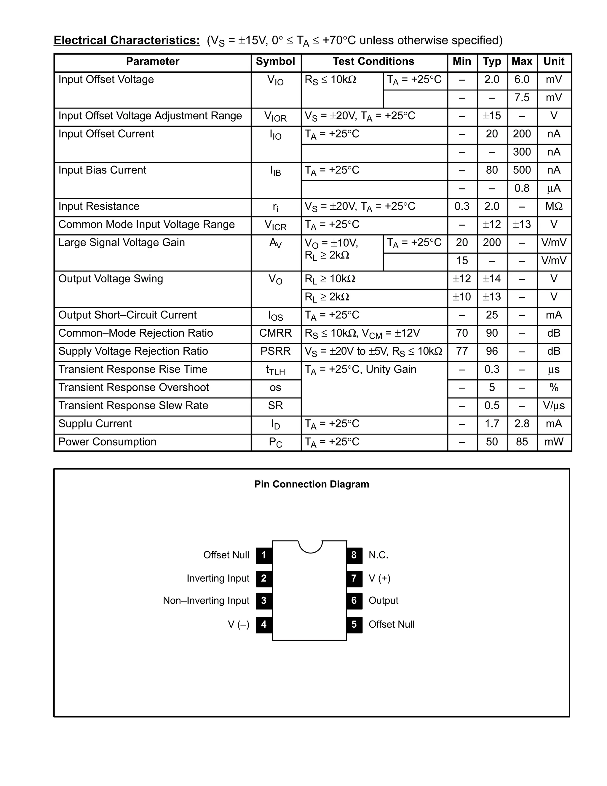


The NTE941M and NTE941SM are general purpose operational amplifiers that offer protection from overloads and oscillations. They have a supply voltage rating of ±18V, can withstand differential input voltages up to ±30V, and provide continuous short-circuit protection on the output. Both models come in 8-pin packages and have typical operating characteristics such as input offset voltage below 7.5mV and voltage gain above 20V/mV.


