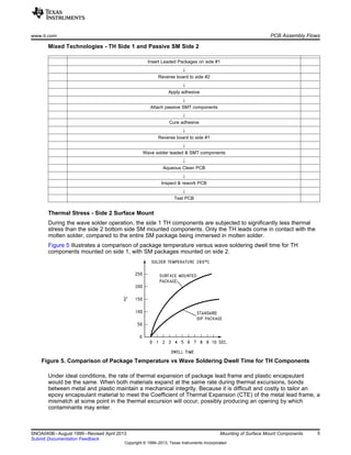
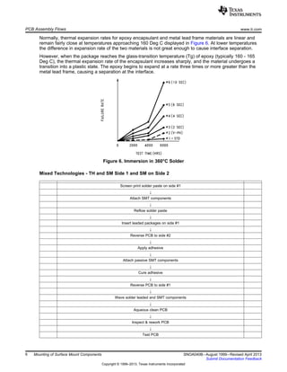
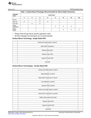
SlideShare a Scribd company logo
1 of 18
Download to read offline
Application Report
SNOA040B–August 1999–Revised April 2013
Mounting of Surface Mount Components
ABSTRACT
Over the past few years, electronic products, and especially those which fall within the category of
Consumer Electronics, have been significantly reduced in physical size and weight. This document
provides information about the techniques used to mount CSP size components.
Contents
1 Introduction .................................................................................................................. 3
2 Component Size Comparison ............................................................................................. 3
3 Accelerated Bias Moisture Test DIP, SO's, and CSP .................................................................. 4
4 PCB Assembly Flows ....................................................................................................... 4
5 Changing Assembly Techniques & Technologies ...................................................................... 8
5.1 Combined Wave Solder and Solder Reflow .................................................................... 8
5.2 Fine Pitch SM Solder Reflow Side 1 and Side 2 ............................................................... 8
6 Purpose of Solder Paste ................................................................................................... 8
6.1 Types Of Solder Paste Fluxes ................................................................................... 8
7 Comparison of Particle Size / Shape of Various Solder Pastes ...................................................... 9
8 Solder Paste For Standard SM Packages ............................................................................... 9
8.1 Solder Paste For Fine Pitch SM Packages ................................................................... 10
8.2 Water Soluble Solder Paste For Fine Pitch Surface Mount Packages .................................... 10
8.3 Stencil Thickness ................................................................................................. 10
8.4 Stencil Materials .................................................................................................. 10
8.5 Squeegee .......................................................................................................... 10
8.6 Print Speed ........................................................................................................ 11
8.7 Print Pressure ..................................................................................................... 11
8.8 Off And On Contact .............................................................................................. 11
8.9 Temperature And Humidity ...................................................................................... 11
8.10 Stencil And Screen Cleaning ................................................................................... 11
9 Component Placement System .......................................................................................... 11
9.1 System Configuration and Specifications ..................................................................... 11
9.2 Placement System ............................................................................................... 12
9.3 Placing Heads ..................................................................................................... 12
9.4 Componet Types ................................................................................................. 12
9.5 Component In-Feeding Systems ............................................................................... 12
9.6 Printed Circuit Board Dimensions .............................................................................. 13
9.7 Vision Assisted Component Placement ....................................................................... 13
9.8 Placement Speed ................................................................................................. 13
9.9 Placement Accuracy ............................................................................................. 13
9.10 Component Pick-Up Head Types .............................................................................. 14
9.11 Component Placement Pressure ............................................................................... 14
10 Convection Reflow Furnace .............................................................................................. 14
11 Techniques of Solder Interconnection .................................................................................. 14
11.1 Local Component Heating ....................................................................................... 14
11.2 Global Board Heating ............................................................................................ 14
11.3 Thermal Processing (Reflow) System ......................................................................... 15
11.4 Product Throughput .............................................................................................. 15
All trademarks are the property of their respective owners.
1
SNOA040B–August 1999–Revised April 2013 Mounting of Surface Mount Components
Submit Documentation Feedback
Copyright © 1999–2013, Texas Instruments Incorporated
www.ti.com
11.5 Thermal Uniformity and Accuracy .............................................................................. 15
11.6 Nitrogen Consumption ........................................................................................... 15
11.7 Infrared Radiation (I.R.) Reflow Soldering .................................................................... 15
11.8 Natural Convection Reflow Soldering .......................................................................... 15
11.9 Forced Convection Reflow Soldering .......................................................................... 15
11.10 Fixed Convection Reflow Soldering ........................................................................... 16
11.11 Heating Zones .................................................................................................... 16
11.12 Active Cooling Zones ............................................................................................ 16
12 PCB Assembly Cleaning ................................................................................................. 16
13 PCB Cleaning Test ........................................................................................................ 16
14 SM Reflow Soldering Reliability ......................................................................................... 16
15 Thermal Characteristics of SM Components .......................................................................... 17
List of Figures
1 Molded Dip, SOIC, CSP - 24 Pin ......................................................................................... 3
2 Molded Dip, SOIC, micro-SMD - 8 Pin................................................................................... 3
3 TSSOP & CSP - 24 pin .................................................................................................... 4
4 Accelerated Environmental Bias Moisture Test Performance......................................................... 4
5 Comparison of Package Temperature vs Wave Soldering Dwell Time for TH Components ..................... 5
6 Immersion in 360°C Solder ................................................................................................ 6
List of Tables
1 Surface Mount Packages Recommended for Wave Solder Immersion ............................................. 7
2 Mounting of Surface Mount Components SNOA040B–August 1999–Revised April 2013
Submit Documentation Feedback
Copyright © 1999–2013, Texas Instruments Incorporated
www.ti.com Introduction
1 Introduction
Products such as cellular telephones, lap-top computers, pagers, and camcorders have been reduced by
as much as 3/4 of their original introductory size and weight. The most significant contributing factor to this
reduction has been the inclusion of fine pitch, Surface Mount (SM) components. The larger, thicker and
heavier leaded Through-Hole (TH) packages consumed far too much power, too much space and
contributed significantly to the total weight of the final product.
Product manufacturers were listening when the customer said "Make it smaller, lighter and less
expensive".
A second phase to this continued reduction in package size and weight is currently being experienced. A
new family of sub-miniature surface mounted packages known under the industry's generic name of Chip
Scale Packages (CSP) have recently been introduced. CSP size components are currently the basis of a
new series of consumer products. CSP components are currently being supplied in two (2) package
configuration, both of which will be a maximum of 1.2 X of the die size. One incorporates planar or
bumped pad interconnections on the peripheral of the package underside. The other package is in the
form of a reduced scale ball grid array either in a partially or fully populated I/O condition.
The increasing availability of the CSP significantly impacts the ability of product designers to design hand-
held products of a size and weight not previously possible. The new CSP allows a higher density of
components to be placed into an increasingly smaller portion of an existing printed circuit board, or that
the printed circuit board may be reduced with an accompanying reduction in product size, weight and cost.
Chip Scale Packages incorporating high I/O dies, along with discrete passive components are currently
used in the design of the palm-sized camcorders. As a residual benefit, with components in closer
proximity the signal propagation time is reduced thus producing a series of faster circuits.
Accompanying the benefits of smaller size, reduced weight, higher density and increased performance,
the individual Methods, Technologies and Techniques used to assemble printed circuit board assemblies
have been impacted.
2 Component Size Comparison
Figure 1. Molded Dip, SOIC, CSP - 24 Pin
Figure 2. Molded Dip, SOIC, micro-SMD - 8 Pin
3
SNOA040B–August 1999–Revised April 2013 Mounting of Surface Mount Components
Submit Documentation Feedback
Copyright © 1999–2013, Texas Instruments Incorporated
Accelerated Bias Moisture Test DIP, SO's, and CSP www.ti.com
The Surface Mount (SM) package was developed to provide the customer with increased component
density and performance over the larger Dual-Inline-Package (DIP). The SM package also provides the
same DIP high reliability.
The Chip Scale Package (CSP) was developed to provide the customer with an additional increase in
component performance and density over the SM package. The CSP also provides the same high
reliability as the DIP and SM package.
Figure 3. TSSOP & CSP - 24 pin
CSP and SM packages at Texas Instrument were internally qualified for production under the condition
that they be of comparable reliability performance to a standard dual in-line package under all accelerated
environmental tests.
3 Accelerated Bias Moisture Test DIP, SO's, and CSP
Figure 4 is a summary of accelerated environmental bias moisture test performance on 15V CMOS and
30V BIPOLAR product assembled in SM and DIP (control) packages.
Figure 4. Accelerated Environmental Bias Moisture Test Performance
4 PCB Assembly Flows
Through-Hole (TH) Technology
Insert Leaded Packages on side #1
↓
Wave solder the leads on side #2
↓
Aqueous Clean PCP
↓
Inspect & Rework PCB
↓
Test PCB
4 Mounting of Surface Mount Components SNOA040B–August 1999–Revised April 2013
Submit Documentation Feedback
Copyright © 1999–2013, Texas Instruments Incorporated
www.ti.com PCB Assembly Flows
Mixed Technologies - TH Side 1 and Passive SM Side 2
Insert Leaded Packages on side #1
↓
Reverse board to side #2
↓
Apply adhesive
↓
Attach passive SMT components
↓
Cure adhesive
↓
Reverse board to side #1
↓
Wave solder leaded & SMT components
↓
Aqueous Clean PCB
↓
Inspect & rework PCB
↓
Test PCB
Thermal Stress - Side 2 Surface Mount
During the wave solder operation, the side 1 TH components are subjected to significantly less thermal
stress than the side 2 bottom side SM mounted components. Only the TH leads come in contact with the
molten solder, compared to the entire SM package being immersed in molten solder.
Figure 5 illustrates a comparison of package temperature versus wave soldering dwell time for TH
components mounted on side 1, with SM packages mounted on side 2.
Figure 5. Comparison of Package Temperature vs Wave Soldering Dwell Time for TH Components
Under ideal conditions, the rate of thermal expansion of package lead frame and plastic encapsulant
would be the same. When both materials expand at the same rate during thermal excursions, bonds
between metal and plastic maintain a mechanical integrity. Because it is difficult and costly to tailor an
epoxy encapsulant material to meet the Coefficient of Thermal Expansion (CTE) of the metal lead frame, a
mismatch at some point in the thermal excursion will occur, possibly producing an opening by which
contaminants may enter.
5
SNOA040B–August 1999–Revised April 2013 Mounting of Surface Mount Components
Submit Documentation Feedback
Copyright © 1999–2013, Texas Instruments Incorporated
PCB Assembly Flows www.ti.com
Normally, thermal expansion rates for epoxy encapsulant and metal lead frame materials are linear and
remain fairly close at temperatures approaching 160 Deg C displayed in Figure 6. At lower temperatures
the difference in expansion rate of the two materials is not great enough to cause interface separation.
However, when the package reaches the glass-transition temperature (Tg) of epoxy (typically 160 - 165
Deg C), the thermal expansion rate of the encapsulant increases sharply, and the material undergoes a
transition into a plastic state. The epoxy begins to expand at a rate three times or more greater than the
metal lead frame, causing a separation at the interface.
Figure 6. Immersion in 360°C Solder
Mixed Technologies - TH and SM Side 1 and SM on Side 2
Screen print solder paste on side #1
↓
Attach SMT components
↓
Reflow solder paste
↓
Insert leaded packages on side #1
↓
Reverse PCB to side #2
↓
Apply adhesive
↓
Attach passive SMT components
↓
Cure adhesive
↓
Reverse PCB to side #1
↓
Wave solder leaded and SMT components
↓
Aqueous clean PCB
↓
Inspect & rework PCB
↓
Test PCB
6 Mounting of Surface Mount Components SNOA040B–August 1999–Revised April 2013
Submit Documentation Feedback
Copyright © 1999–2013, Texas Instruments Incorporated
www.ti.com PCB Assembly Flows
Table 1. Surface Mount Packages Recommended for Wave Solder Immersion
Package
Lead Count
Type
3 4 5 6 8 14 16 20
SC-70 X
SOT-23 X X X
SOT-223 X X
SOIC -
X X X
NARROW
SOIC -
X X X
WIDE
• Please verify through device specific application notes.
• All other packages and lead types are not recommended.
Surface Mount Technology - Single Sided PCB
Screen print solder paste on side #1
↓
Attach SMT components
↓
Reflow solder paste
↓
Aqueous clean PCB
↓
Inspect & rework PCB
↓
Test PCB
Surface Mount Technologies - Double Sided PCB
Screen print solder paste on side #1
↓
Apply adhesive on side #1
↓
Attach SMT components on side #1
↓
Cure adhesive on side #1
↓
Reverse PCB to side #2
↓
Screen print solder paste on side #2
↓
Attach SMT components on side #2
↓
Reflow solder paste (both sides)
↓
Aqueous clean PCB
↓
Inspect & rework PCB
↓
Test PCB
7
SNOA040B–August 1999–Revised April 2013 Mounting of Surface Mount Components
Submit Documentation Feedback
Copyright © 1999–2013, Texas Instruments Incorporated
Changing Assembly Techniques & Technologies www.ti.com
5 Changing Assembly Techniques & Technologies
5.1 Combined Wave Solder and Solder Reflow
More mature products incorporating printed circuit boards designed with Through-Hole (TH)
semiconductors in a Dual-In-Line (DIP) package and with TH axial leaded components, require bottom
side board wave soldering for component to pad interconnection.
Specified packages (see Table 1) may be mounted on the underside (side 2) of the board using this same
solder attachment technique. This assembly technique allows better utilization of the PCB underside, thus
freeing up top side real estate for high lead count active components.
Securement of the bottom side (side 2) SM components is achieved through the use of a cured adhesive
applied prior to the wave soldering application. Component Engineers responsible for components
selected for bottom side SM mounted components had to take into consideration that these components
were subjected to the same time and temperature wave soldering profile experienced by only the leads of
leaded TH components and selected these SM components accordingly.
5.2 Fine Pitch SM Solder Reflow Side 1 and Side 2
Fine pitch SM components are routinely mounted both on side 1 and side 2 with no use of adhesive. The
one exception to this rule is when the component possesses a larger body mass in relation to the strength
of the total volume of solder paste incorporated in the component interconnection.
6 Purpose of Solder Paste
Solder paste provides both the metals and the cleaning agent used to produce the pad interconnection of
package lead to printed circuit board pad.
The purpose of the fluxing system within the paste is to provide clean, positive wettable surfaces to which
the metal solder bonds, thus allowing the electrical interconnection to be produced. The fluxing system
operates as the cleaning agent required to remove potential oxides from both the package lead/pad and
the board pad. The fluxing system also provides protection of the newly cleaned metal surfaces from re-
oxidation during the soldering operation while the lead and pad is at their highest temperature.
6.1 Types Of Solder Paste Fluxes
The fluxing system is composed of a flux and binder system used in solder paste, and is generally divided
into the categories of Rosin-based, Water Soluble and No-Clean.
Rosin-based fluxes are designated
R Rosin, non-activated
RMA Rosin, mildly activated
RA Rosin, fully activated
Water Soluble fluxes are designated
WS Water-soluble
No-Clean fluxes are designated
NC No-Cleaning required
8 Mounting of Surface Mount Components SNOA040B–August 1999–Revised April 2013
Submit Documentation Feedback
Copyright © 1999–2013, Texas Instruments Incorporated
www.ti.com Comparison of Particle Size / Shape of Various Solder Pastes
7 Comparison of Particle Size / Shape of Various Solder Pastes
200 x Alpha (62/36/2) 200 x Kester (63/37)
Solder Paste Screened on Pads 200 x ESL (63/37)
8 Solder Paste For Standard SM Packages
Consistency and uniformity is the key for any successful solder paste material. The basic requirement is a
stable and homogeneous blend of atomized metal alloy combined with a flux, binder, and solvent system
which eliminates the possibility of later separation of the respective materials. These qualities are required
to ensure a predicable screening and stenciling printing operation producing the required pattern
definition.
The selected solder paste should be formulated so as to eliminate potential breakdown of the metal, flux,
binder, and solvents combination, or the premature drying of the solder paste on the printer. Both of the
previously cited qualities should be in addition to providing a minimum of 48 hours tack time. The selected
solder paste should be formulated so as to prevent slump and provide over 8 hours of screen working life,
with no presence of skipping, scooping and clumping during printing.
For screen printing of standard pitch SM packages, the metal alloy powders should be spherical is shape
with a minimal oxide content and screened to 45-75 micron particle size. The paste should contain a
minimum of 88% to 90% metal content, and have a viscosity of 500,000 to 600,000 centipoise.
For stencil printing of standard pitch SM packages, the metal alloy powders shape, size and content
should remain the same but the viscosity should be increased to 700,000 or 800,000 centipoise.
9
SNOA040B–August 1999–Revised April 2013 Mounting of Surface Mount Components
Submit Documentation Feedback
Copyright © 1999–2013, Texas Instruments Incorporated
Solder Paste For Standard SM Packages www.ti.com
In most cases, R, RMA and RA rosin-based fluxes will normally be removed using an aqueous de-ionized
heated water cleaning system, augmented with a saponifier or another surfactant additive. The resultant
cleaning water should produce biodegradable saponified products.
8.1 Solder Paste For Fine Pitch SM Packages
Those solder pastes specifically designed for high lead count, fine pitch packages with lead spacing of
0.015" require a unique formulation for stenciling, screening and automatic point to point dispensing.
Solder pastes specifically formulated for fine pitch SM components should incorporate all of the previously
cited qualities, plus a flux system developed specifically to ensure that no slumping while still in the wet
stage. Fine pitch solder paste should not produce bridging, shorting or solder balling when the paste
experiences the reflow.
As is in the case of Standard Pitch SM components, R, RMA and RA rosin-based fluxes will normally be
removed using hot de-ionized water, augmented with a surfactant or other additive.
8.2 Water Soluble Solder Paste For Fine Pitch Surface Mount Packages
Water soluble solder pastes should display all of the stencil or screen printing qualities displayed by
conventional rosin-based pastes, but should also eliminate the need for chlorofluorocarbons,
chlorocarbons or other solvent blends sometimes used for rosin-based flux residue removal.
Although they are soluble in water, water soluble pastes should not be hygroscopic and should be
formulated to provide up to 8 hours of screen working life and 48 hours of tack time similar to rosin-based
pastes.
Water soluble, fine solder pastes should be halogen-free. The water-soluble residues should be capable of
being cleaned to the extent that they are equivalent in performance, water extract resistivity and SIR
values to standard RMA fluxes. Flux residues should be able to be removed with a cool presoak followed
by a 140 Deg. F spray.
8.3 Stencil Thickness
SM Lead Pitch
inch mm
0.050 1.27
0.025 0.63
0.015 to 0.020 0.4 to 0.5
Recommended Stencil Thickness
inch mm
0.008 to 0.010 0.20 to 0.25
0.006 to 0.008 0.15 to 0.20
0.004 to 0.006 0.10 to 0.15
8.4 Stencil Materials
Stainless Steel is the most prevalent material used to produce stencils, but brass, Alloy 42, molybdenum
and nickel plated brass are also used.
8.5 Squeegee
Metal is the most common material used to produce squeegees. The justification for the use of metal is
that it produces a uniform surface across the top surface of the stencil without scooping down into the just
deposited solder paste.
Rubber of an 80 to 90 Durometer reading is also used.
10 Mounting of Surface Mount Components SNOA040B–August 1999–Revised April 2013
Submit Documentation Feedback
Copyright © 1999–2013, Texas Instruments Incorporated
www.ti.com Component Placement System
8.6 Print Speed
Printing speeds of 0.5 to 2.5 inches (15 to 65 mm) per second are normally used, depending on type and
capabilities of the solder printing machine.
8.7 Print Pressure
During the solder paste printing operation, sufficient downward pressure should be exerted by the
squeegee against the stencil surface to wipe the stencil clean. Although the printing pressure will vary with
the type of printer, typically a pressure of 1.25 to 2.5 lbs per inch of squeegee length is acceptable.
8.8 Off And On Contact
Both contact and non-contact techniques are used successfully. If non-contact is used, a snap-off of up to
0.005 is recommended.
8.9 Temperature And Humidity
The screen printing of solder paste should be performed between a temperature of 68° to 78° F (20° to
26° C). The relative humidity of the application area should be kept between 35% to 65%. Solder paste
not applied to printed circuit boards should not be returned to the container from which it was taken.
8.10 Stencil And Screen Cleaning
Stencils and screens should be cleaned of unused solder paste using water heated to a minimum of 140
Deg F in conjunction with a pressure spray. Although the initial water need not be deionized, it is
recommended that a final rinse be performed using deionized water, followed by an isopropanol rinse.
This same procedure should also be followed for any hand tools and the squeegee used to apply the
solder paste.
At no time should the stencil, screen or tools which have come in contact with unreflowed solder paste be
cleaned in equipment used to clean printed circuit boards of reflowed solder paste residues.
9 Component Placement System
9.1 System Configuration and Specifications
Product designs continue to demand continued down-sizing of the component package, accompanied by
higher board densities. The component placement system must accommodate these trends by employing
a highly accurate, computer controlled, camera directed placement nozzle that is responsible for
constraining the component during pick-up through push-off after placement.
Following are some of the more significant elements devised by the system vendors there by enabling the
placement system to produce high speed, high density accurate component placements:
• Computer controller
• Windows or vendor software
• Vision correction system
• Component body height adjustment
• Z-Axis placement programmability
• Single Head - Multiple programmable nozzles
• Dual Head - Multiple programmable nozzles
• Dual Head - 6 nozzles per head
• Dual Work Table - 12 heads with 3 nozzles per head
11
SNOA040B–August 1999–Revised April 2013 Mounting of Surface Mount Components
Submit Documentation Feedback
Copyright © 1999–2013, Texas Instruments Incorporated
Component Placement System www.ti.com
9.2 Placement System
9.3 Placing Heads
9.4 Componet Types
The types of components which may be placed are generally only restricted by the types of feeders that
may be may be interfaced to the placement system. Following are some representative component types
which are being automatically picked and placed by placement systems of the latest design:
• Chips
• CSP
• QFP
• TAB
• BGA
• MELF
• SOIC
• PLCC
• TSOP
• TSSOP
• Flip Chip
9.5 Component In-Feeding Systems
With the introduction of the embossed (pocketed) tape, more package types are being supplied in this
format due to increased end-user demand. The embossed tape provides the end-user the ability to
maintain an improved quantity and quality control through the use of the see-through tape and the rigid
cardboard sidewalls of the shipping reel. Paper tape is normally only used to provide the smallest types
and values of discrete, passive components.
• 8 mm paper tape
• 8 mm embossed tape
• 12 mm embossed tape
12 Mounting of Surface Mount Components SNOA040B–August 1999–Revised April 2013
Submit Documentation Feedback
Copyright © 1999–2013, Texas Instruments Incorporated
www.ti.com Component Placement System
• 16 mm embossed tape
• 24 mm embossed tape
• 32 mm embossed tape
• 48 mm embossed tape
• Stick in-feeding
• Tray in-feeding
• Ultra-small chips up to 4.5 mm
• Medium-sized odd form components up to 28.0 mm
• Large odd form components up to 38.0 mm
• Extremely large odd form components up to 74.0 mm
9.6 Printed Circuit Board Dimensions
Current placement systems are designed to provide the end user with the maximum printed circuit board
size in both the X and Y axis. Most of the current designs will allow a change in the conveyor rail width to
be automatically executed by servo motors by program commands conveyed through the computer
controller.
• Min. 80 x 50 mm (3 x 2")
• Max. 508 x 457 mm (20 x 18")
9.7 Vision Assisted Component Placement
The vision system should include as a basis element of the design, an ability to process (establish
X/Y/Theta) the component location on the pick-up head and match the component to the respective
component pads. To achieve the required placement accuracy, the following is necessary:
• Gray scale vision processing
• Component placement algorithms
• Fiducial (local and global) camera
• Component pad/lead recognition camera
9.8 Placement Speed
Although placement speed is typically quoted at approximately 0.1 second per placement, Flip Chip
components can take as long as 3.5 to 5.0 seconds per shot (placement). Component placement speed is
dependent upon such factors as distance which the placement head must travel between component pick-
up and placement location, and the requirement to view the component leads/pads for component-to-pad
alignment prior to placement
• Min. 0. 09 sec. per component
• Max. 0. 12 sec. per component
9.9 Placement Accuracy
The accuracy to which the component is aligned and placed on the solder pads is contingent upon several
factors, such as use of local fiducial marks; datum point location; size of printed circuit board; and flatness
of printed circuit board.
• Min. ± 0.025 mm (using local fiducial marks)
• Max. ± 0.1 mm
13
SNOA040B–August 1999–Revised April 2013 Mounting of Surface Mount Components
Submit Documentation Feedback
Copyright © 1999–2013, Texas Instruments Incorporated
Convection Reflow Furnace www.ti.com
9.10 Component Pick-Up Head Types
The most favored technique of component pick-up is via the vacuum nozzle due to the system's ability to
create a negative pressure instantly upon making contact with the top surface of the component with the
soft rubber nozzle contact, and then reverse the process by producing a positive pressure to "blow" the
component off the nozzle upon placement. Mechanical chucks, although favored for some time, are
expensive to maintain and do present some mechanical difficulties in their operation.
• Vacuums nozzles
• Mechanical chucks
9.11 Component Placement Pressure
Programmable placement pressure can be specified for each component, enabling placement of very
delicate parts.
10 Convection Reflow Furnace
11 Techniques of Solder Interconnection
Solder interconnection of Through-Hole and Surface Mount components to printed circuit boards may be
classified as using the following two categories:
11.1 Local Component Heating
Local heating can be divided into the following methods:
• Hot plates with solder paste or flux
• Hand solder iron with solder and flux
• Hot bar (pulsed heater) using solder paste or flux
• Hot air gun using solder paste or flux
• Directed laser energy using solder paste or flux
11.2 Global Board Heating
Global heating is divided into the following methods:
• Solder submersion
• Directed IR reflow using solder paste
• Hot air furnace reflow using solder paste
• Vapor phase reflow using solder paste
• Convection furnace reflow using solder paste
As is displayed by the various soldering techniques above, solder paste is the dominant method of
attaching electrical components to printed circuit boards.
14 Mounting of Surface Mount Components SNOA040B–August 1999–Revised April 2013
Submit Documentation Feedback
Copyright © 1999–2013, Texas Instruments Incorporated
www.ti.com Techniques of Solder Interconnection
11.3 Thermal Processing (Reflow) System
In a similar fashion as in the case of the component placement system, the specifications for thermal
processing system will be developed based upon the anticipated reflow soldering requirements throughout
the life of the oven. This statement is true for not only the type and configuration of the components
currently being soldered, but also any adhesive which would require curing.
Taken into consideration will be whether the components of a surface mount design are leaded or
leadless the physical size and robustness of the component to withstand reflow temperatures. Because
most components being designed into today's products are of a reduced mechanical configuration and
located in close proximity to each other on smaller printed boards, the selection of the technology used
within the reflow system becomes even more critical.
Following are only some of the more critical decisions which will be made concerning the more pertinent
parameters of the thermal processing system selection:
11.4 Product Throughput
Is the reflow oven "sized" for the current and anticipated production requirements. This will require not
only a determination as to the number of boards the oven will process, but also how the boards will be
conveyed through the oven.
11.5 Thermal Uniformity and Accuracy
The reflow system should provide a uniform heat transfer from the heating source, distributing it evenly
over the product surfaces under process in an accurate manner so that all of the board surfaces receives
an equal temperature rise. The same criteria is required for cooling.
11.6 Nitrogen Consumption
The infusion of nitrogen immediately prior to and during the solder paste reflow operation is mandated by
the process and materials being assembled. Specifically, bare-copper circuit boards, and no-clean solder
pastes benefit from the inclusion of the nitrogen atmosphere.
Certain No-Clean solder paste with a metal alloy content of greater than 98% will often require the use of
Nitrogen because the remaining 2% (by weight) or less will contain an insufficient amount of flux material
available to prevent oxidation of the soldered elements if reflowed in an air environment.
Should the process and materials being assembled require nitrogen, features within the oven design
should be present which minimizes nitrogen consumption during preheat, soak, reflow, and cool.
11.7 Infrared Radiation (I.R.) Reflow Soldering
Radiant I.R. is a direct, focused heat source and was the initial heating technique used by the electronics
industry to reflow solder paste. This technique, when not properly adjusted in relation to the board
distance, could allow excessive amounts of directly focused heat to be delivered to the surface of the
board producing a scorching effect to the board and the components under reflow.
This technique is no longer commercially viable.
11.8 Natural Convection Reflow Soldering
Natural convection of the heat required to reflow the solder is normally obtained through the use of a non-
focused I.R. source, without the benefit of a forced air circulation. This design is often referred to as "non-
focused", with the efficiency capability rated lower than the forced convection design due to the ability of
larger components to shield smaller components from the available heat source.
11.9 Forced Convection Reflow Soldering
Heat require to reflow the solder paste is achieved by directing I.R. energy towards a metal or ceramic
surface and utilizing the convected (radiated) energy from the opposite surface to produce the reflow.
15
SNOA040B–August 1999–Revised April 2013 Mounting of Surface Mount Components
Submit Documentation Feedback
Copyright © 1999–2013, Texas Instruments Incorporated
PCB Assembly Cleaning www.ti.com
The heat is circulated within the reflow zones by strategically located fans. By use of a non-directed,
convected heat circulated via strategically located fans, hot spots on the boards can potentially be
eliminated.
11.10 Fixed Convection Reflow Soldering
Fixed Convection reflow soldering utilizes much of the same technology as Forced Convection with the
exception of the use of strategically located fans.
11.11 Heating Zones
The number of heating zones required will be determined by current and anticipated product throughput
requirements, product size and physical mass, product orientation within the oven while on the conveyor,
and requirements dictated by the particular solder paste reflow profile. Reflow ovens are typically offered
in ranges from four to 12 heating zones.
11.12 Active Cooling Zones
Active cooling zones should be positioned immediately adjacent to the heating zones and should be
ideally provided to meet the reflow requirements specified by the solder paste manufacturer.
The amount of cooling required may also be dictated by product handling or subsequent assembly
operations following reflow.
Depending on the system requirements and vendor capability, the number of cooling zones which may be
incorporated into the system may range from one to 12.
12 PCB Assembly Cleaning
If the printed circuit boards were assembled using a rosin based or other flux system which requires
removal from the board surface after reflow, the subsequent cleaning operation should be performed as
shortly after reflow as possible.
The timely initiation of the cleaning operation is dictated by the ability of the flux to collect and harden with
additional residues under and around traces and the bodies of components. The lack of attention to the
timely removal of this residue present additional and unneeded removal difficulties, with the possibility that
some contaminates may be trapped in flux and remain on the surface of the board to potentially
compromise qualities for the finished product.
13 PCB Cleaning Test
Upon completion of the solder reflow operation, the surface mount assembly should be tested for ionic
and other contaminates using recognized specification, such as IPC-6012.
If the printed circuit board is to have a permanent solder mask coating applied, the bare uncoated board
should be also tested for ionic and other contaminates prior to permanent coating.
14 SM Reflow Soldering Reliability
More recently designed products utilizing the low profile, high lead count, fine pitch SM components, when
combined with Chip Scale Packages present additional challenges to the techniques and technologies of
high reliability component interconnection.
The potential obstacles of high reliability fine pitch SM and reduced size CSP component interconnections
are contingent upon a number of parameters, with the most prevalent being the following:
• Technology and package construction
• Quality and repeatability of the reflow process
• Metallurgy and uniformity of both the solder paste and interconnection pad plating
• Individual board design, both internally and externally
• Conditions in which the product will be used
• The intended product life
16 Mounting of Surface Mount Components SNOA040B–August 1999–Revised April 2013
Submit Documentation Feedback
Copyright © 1999–2013, Texas Instruments Incorporated
www.ti.com Thermal Characteristics of SM Components
Reliability level demands are higher for products using the new low profile, fine-pitch, high lead count
miniature IC packages, such as CSP and reduced size BGA over assemblies built around older, more
conventional packages with their longer and more compliant leads.
15 Thermal Characteristics of SM Components
Both Chip Scale Packages and SM components are typically fabricated using a combination of either a
metal lead frame; laminated substrate; ceramic substrate, or flexible film substrate as a base on which a
die is adhesively attached. Gold wires are bonded from die to lead frame/substrate, and the unit is
encapsulated, with a thermoset epoxy.
Because each material has different rate of thermal expansion, the thermal characteristics of the materials
generally correspond to a Thermal Mechanical Analysis (TMA) graph.
17
SNOA040B–August 1999–Revised April 2013 Mounting of Surface Mount Components
Submit Documentation Feedback
Copyright © 1999–2013, Texas Instruments Incorporated
IMPORTANT NOTICE
Texas Instruments Incorporated and its subsidiaries (TI) reserve the right to make corrections, enhancements, improvements and other
changes to its semiconductor products and services per JESD46, latest issue, and to discontinue any product or service per JESD48, latest
issue. Buyers should obtain the latest relevant information before placing orders and should verify that such information is current and
complete. All semiconductor products (also referred to herein as “components”) are sold subject to TI’s terms and conditions of sale
supplied at the time of order acknowledgment.
TI warrants performance of its components to the specifications applicable at the time of sale, in accordance with the warranty in TI’s terms
and conditions of sale of semiconductor products. Testing and other quality control techniques are used to the extent TI deems necessary
to support this warranty. Except where mandated by applicable law, testing of all parameters of each component is not necessarily
performed.
TI assumes no liability for applications assistance or the design of Buyers’ products. Buyers are responsible for their products and
applications using TI components. To minimize the risks associated with Buyers’ products and applications, Buyers should provide
adequate design and operating safeguards.
TI does not warrant or represent that any license, either express or implied, is granted under any patent right, copyright, mask work right, or
other intellectual property right relating to any combination, machine, or process in which TI components or services are used. Information
published by TI regarding third-party products or services does not constitute a license to use such products or services or a warranty or
endorsement thereof. Use of such information may require a license from a third party under the patents or other intellectual property of the
third party, or a license from TI under the patents or other intellectual property of TI.
Reproduction of significant portions of TI information in TI data books or data sheets is permissible only if reproduction is without alteration
and is accompanied by all associated warranties, conditions, limitations, and notices. TI is not responsible or liable for such altered
documentation. Information of third parties may be subject to additional restrictions.
Resale of TI components or services with statements different from or beyond the parameters stated by TI for that component or service
voids all express and any implied warranties for the associated TI component or service and is an unfair and deceptive business practice.
TI is not responsible or liable for any such statements.
Buyer acknowledges and agrees that it is solely responsible for compliance with all legal, regulatory and safety-related requirements
concerning its products, and any use of TI components in its applications, notwithstanding any applications-related information or support
that may be provided by TI. Buyer represents and agrees that it has all the necessary expertise to create and implement safeguards which
anticipate dangerous consequences of failures, monitor failures and their consequences, lessen the likelihood of failures that might cause
harm and take appropriate remedial actions. Buyer will fully indemnify TI and its representatives against any damages arising out of the use
of any TI components in safety-critical applications.
In some cases, TI components may be promoted specifically to facilitate safety-related applications. With such components, TI’s goal is to
help enable customers to design and create their own end-product solutions that meet applicable functional safety standards and
requirements. Nonetheless, such components are subject to these terms.
No TI components are authorized for use in FDA Class III (or similar life-critical medical equipment) unless authorized officers of the parties
have executed a special agreement specifically governing such use.
Only those TI components which TI has specifically designated as military grade or “enhanced plastic” are designed and intended for use in
military/aerospace applications or environments. Buyer acknowledges and agrees that any military or aerospace use of TI components
which have not been so designated is solely at the Buyer's risk, and that Buyer is solely responsible for compliance with all legal and
regulatory requirements in connection with such use.
TI has specifically designated certain components as meeting ISO/TS16949 requirements, mainly for automotive use. In any case of use of
non-designated products, TI will not be responsible for any failure to meet ISO/TS16949.
Products Applications
Audio www.ti.com/audio Automotive and Transportation www.ti.com/automotive
Amplifiers amplifier.ti.com Communications and Telecom www.ti.com/communications
Data Converters dataconverter.ti.com Computers and Peripherals www.ti.com/computers
DLP® Products www.dlp.com Consumer Electronics www.ti.com/consumer-apps
DSP dsp.ti.com Energy and Lighting www.ti.com/energy
Clocks and Timers www.ti.com/clocks Industrial www.ti.com/industrial
Interface interface.ti.com Medical www.ti.com/medical
Logic logic.ti.com Security www.ti.com/security
Power Mgmt power.ti.com Space, Avionics and Defense www.ti.com/space-avionics-defense
Microcontrollers microcontroller.ti.com Video and Imaging www.ti.com/video
RFID www.ti-rfid.com
OMAP Applications Processors www.ti.com/omap TI E2E Community e2e.ti.com
Wireless Connectivity www.ti.com/wirelessconnectivity
Mailing Address: Texas Instruments, Post Office Box 655303, Dallas, Texas 75265
Copyright © 2013, Texas Instruments Incorporated

More Related Content

What's hot

The Effect of CPU Clock Rate on Power Consumption
The Effect of CPU Clock Rate on Power ConsumptionThe Effect of CPU Clock Rate on Power Consumption
The Effect of CPU Clock Rate on Power ConsumptionMarc Bacvanski
 
Overview of the_maisotsenko_cycle_a_way
Overview of the_maisotsenko_cycle_a_wayOverview of the_maisotsenko_cycle_a_way
Overview of the_maisotsenko_cycle_a_wayShamkant Mirashi
 
Sustainable and Resilient Playground_FinalReport_5-11-2016 (1)
Sustainable and Resilient Playground_FinalReport_5-11-2016 (1)Sustainable and Resilient Playground_FinalReport_5-11-2016 (1)
Sustainable and Resilient Playground_FinalReport_5-11-2016 (1)Evan Katzen
 
Economics of wind_energy__march_2009_
Economics of wind_energy__march_2009_Economics of wind_energy__march_2009_
Economics of wind_energy__march_2009_Dr Lendy Spires
 
Estimate For Bpo And Animation Studio
Estimate For Bpo And Animation StudioEstimate For Bpo And Animation Studio
Estimate For Bpo And Animation StudioRaju Nair
 
Energy Systems Optimization Of A Shopping Mall
Energy Systems Optimization Of A Shopping MallEnergy Systems Optimization Of A Shopping Mall
Energy Systems Optimization Of A Shopping MallAristotelisGiannopoulos
 
assign energy storage COMPLETE
assign energy storage COMPLETEassign energy storage COMPLETE
assign energy storage COMPLETEsteven sweeney
 
Solar Thermal Collectors Applications
Solar Thermal Collectors ApplicationsSolar Thermal Collectors Applications
Solar Thermal Collectors ApplicationsH Janardan Prabhu
 
Program Directory For CBPDO Installation and ServerPac Reference z/OS
Program Directory For CBPDO Installation and ServerPac Reference z/OSProgram Directory For CBPDO Installation and ServerPac Reference z/OS
Program Directory For CBPDO Installation and ServerPac Reference z/OSIBM India Smarter Computing
 
Deployment guide series ibm tivoli composite application manager for web reso...
Deployment guide series ibm tivoli composite application manager for web reso...Deployment guide series ibm tivoli composite application manager for web reso...
Deployment guide series ibm tivoli composite application manager for web reso...Banking at Ho Chi Minh city
 
Sustainable heating and cooling
Sustainable heating and coolingSustainable heating and cooling
Sustainable heating and coolingLeonardo ENERGY
 
EMC NetWorker Module for Microsoft SQL Server Release 5.1 ...
EMC NetWorker Module for Microsoft SQL Server Release 5.1 ...EMC NetWorker Module for Microsoft SQL Server Release 5.1 ...
EMC NetWorker Module for Microsoft SQL Server Release 5.1 ...webhostingguy
 
Jboss4 clustering
Jboss4 clusteringJboss4 clustering
Jboss4 clusteringshahdullah
 

What's hot (17)

The Effect of CPU Clock Rate on Power Consumption
The Effect of CPU Clock Rate on Power ConsumptionThe Effect of CPU Clock Rate on Power Consumption
The Effect of CPU Clock Rate on Power Consumption
 
Overview of the_maisotsenko_cycle_a_way
Overview of the_maisotsenko_cycle_a_wayOverview of the_maisotsenko_cycle_a_way
Overview of the_maisotsenko_cycle_a_way
 
Sustainable and Resilient Playground_FinalReport_5-11-2016 (1)
Sustainable and Resilient Playground_FinalReport_5-11-2016 (1)Sustainable and Resilient Playground_FinalReport_5-11-2016 (1)
Sustainable and Resilient Playground_FinalReport_5-11-2016 (1)
 
Economics of wind_energy__march_2009_
Economics of wind_energy__march_2009_Economics of wind_energy__march_2009_
Economics of wind_energy__march_2009_
 
Estimate For Bpo And Animation Studio
Estimate For Bpo And Animation StudioEstimate For Bpo And Animation Studio
Estimate For Bpo And Animation Studio
 
HVDC Grid Feasibility Study
HVDC Grid Feasibility StudyHVDC Grid Feasibility Study
HVDC Grid Feasibility Study
 
Copper for Busbars
Copper for BusbarsCopper for Busbars
Copper for Busbars
 
Energy Systems Optimization Of A Shopping Mall
Energy Systems Optimization Of A Shopping MallEnergy Systems Optimization Of A Shopping Mall
Energy Systems Optimization Of A Shopping Mall
 
assign energy storage COMPLETE
assign energy storage COMPLETEassign energy storage COMPLETE
assign energy storage COMPLETE
 
Memory Pools for C and C++
Memory Pools for C and C++Memory Pools for C and C++
Memory Pools for C and C++
 
Solar Thermal Collectors Applications
Solar Thermal Collectors ApplicationsSolar Thermal Collectors Applications
Solar Thermal Collectors Applications
 
Program Directory For CBPDO Installation and ServerPac Reference z/OS
Program Directory For CBPDO Installation and ServerPac Reference z/OSProgram Directory For CBPDO Installation and ServerPac Reference z/OS
Program Directory For CBPDO Installation and ServerPac Reference z/OS
 
Deployment guide series ibm tivoli composite application manager for web reso...
Deployment guide series ibm tivoli composite application manager for web reso...Deployment guide series ibm tivoli composite application manager for web reso...
Deployment guide series ibm tivoli composite application manager for web reso...
 
Sustainable heating and cooling
Sustainable heating and coolingSustainable heating and cooling
Sustainable heating and cooling
 
A practical guide to tivoli sa nergy sg246146
A practical guide to tivoli sa nergy sg246146A practical guide to tivoli sa nergy sg246146
A practical guide to tivoli sa nergy sg246146
 
EMC NetWorker Module for Microsoft SQL Server Release 5.1 ...
EMC NetWorker Module for Microsoft SQL Server Release 5.1 ...EMC NetWorker Module for Microsoft SQL Server Release 5.1 ...
EMC NetWorker Module for Microsoft SQL Server Release 5.1 ...
 
Jboss4 clustering
Jboss4 clusteringJboss4 clustering
Jboss4 clustering
 

Similar to Snoa040b

Raffaele Salvucci s111179 Thesis
Raffaele Salvucci s111179 ThesisRaffaele Salvucci s111179 Thesis
Raffaele Salvucci s111179 Thesisraffaele00
 
Supercoducting Cables in Grid
Supercoducting Cables in GridSupercoducting Cables in Grid
Supercoducting Cables in Gridprajesh88
 
Semester Project 3: Security of Power Supply
Semester Project 3: Security of Power SupplySemester Project 3: Security of Power Supply
Semester Project 3: Security of Power SupplySøren Aagaard
 
Broadband report
Broadband reportBroadband report
Broadband reportherooftit
 
Design Guide for Rural Substations
Design Guide for Rural SubstationsDesign Guide for Rural Substations
Design Guide for Rural Substationsegua1535
 
Emerging Technologies for Energy Savings Performance Contracting in the Feder...
Emerging Technologies for Energy Savings Performance Contracting in the Feder...Emerging Technologies for Energy Savings Performance Contracting in the Feder...
Emerging Technologies for Energy Savings Performance Contracting in the Feder...Tony Loup
 
Combined heat and power design guide by ASHRAE
Combined heat and power design guide by ASHRAECombined heat and power design guide by ASHRAE
Combined heat and power design guide by ASHRAEAli Hasimi Pane
 
Asu December 2010 Application For Bio Pcm
Asu December 2010 Application For Bio PcmAsu December 2010 Application For Bio Pcm
Asu December 2010 Application For Bio Pcmenergy4you
 
Ampacity according to iec 60287
Ampacity according to iec 60287Ampacity according to iec 60287
Ampacity according to iec 60287azzaabo
 
Worcester Art Museum: Green Technology Evaluation
Worcester Art Museum: Green Technology EvaluationWorcester Art Museum: Green Technology Evaluation
Worcester Art Museum: Green Technology EvaluationFlanna489y
 
Gdfs sg246374
Gdfs sg246374Gdfs sg246374
Gdfs sg246374Accenture
 
Brunel MSc Thesis-NA Stogiannos-Final
Brunel MSc Thesis-NA Stogiannos-FinalBrunel MSc Thesis-NA Stogiannos-Final
Brunel MSc Thesis-NA Stogiannos-FinalAlex Stogiannos
 
Simplified design of reinforced concrete buildings
Simplified design of reinforced concrete buildings Simplified design of reinforced concrete buildings
Simplified design of reinforced concrete buildings Sarmed Shukur
 
Guidelines cdbus
Guidelines cdbusGuidelines cdbus
Guidelines cdbusMeg Cereno
 

Similar to Snoa040b (20)

S E I Passive House
S E I Passive HouseS E I Passive House
S E I Passive House
 
The sustainablesubstationconcept
The sustainablesubstationconceptThe sustainablesubstationconcept
The sustainablesubstationconcept
 
Raffaele Salvucci s111179 Thesis
Raffaele Salvucci s111179 ThesisRaffaele Salvucci s111179 Thesis
Raffaele Salvucci s111179 Thesis
 
Supercoducting Cables in Grid
Supercoducting Cables in GridSupercoducting Cables in Grid
Supercoducting Cables in Grid
 
Semester Project 3: Security of Power Supply
Semester Project 3: Security of Power SupplySemester Project 3: Security of Power Supply
Semester Project 3: Security of Power Supply
 
Broadband report
Broadband reportBroadband report
Broadband report
 
Design Guide for Rural Substations
Design Guide for Rural SubstationsDesign Guide for Rural Substations
Design Guide for Rural Substations
 
Emerging Technologies for Energy Savings Performance Contracting in the Feder...
Emerging Technologies for Energy Savings Performance Contracting in the Feder...Emerging Technologies for Energy Savings Performance Contracting in the Feder...
Emerging Technologies for Energy Savings Performance Contracting in the Feder...
 
Combined heat and power design guide by ASHRAE
Combined heat and power design guide by ASHRAECombined heat and power design guide by ASHRAE
Combined heat and power design guide by ASHRAE
 
Asu December 2010 Application For Bio Pcm
Asu December 2010 Application For Bio PcmAsu December 2010 Application For Bio Pcm
Asu December 2010 Application For Bio Pcm
 
Ampacity according to iec 60287
Ampacity according to iec 60287Ampacity according to iec 60287
Ampacity according to iec 60287
 
Worcester Art Museum: Green Technology Evaluation
Worcester Art Museum: Green Technology EvaluationWorcester Art Museum: Green Technology Evaluation
Worcester Art Museum: Green Technology Evaluation
 
CDP FINAL REPORT
CDP FINAL REPORTCDP FINAL REPORT
CDP FINAL REPORT
 
Gdfs sg246374
Gdfs sg246374Gdfs sg246374
Gdfs sg246374
 
Brunel MSc Thesis-NA Stogiannos-Final
Brunel MSc Thesis-NA Stogiannos-FinalBrunel MSc Thesis-NA Stogiannos-Final
Brunel MSc Thesis-NA Stogiannos-Final
 
Simplified design of reinforced concrete buildings
Simplified design of reinforced concrete buildings Simplified design of reinforced concrete buildings
Simplified design of reinforced concrete buildings
 
32412865.pdf
32412865.pdf32412865.pdf
32412865.pdf
 
Guidelines cdbus
Guidelines cdbusGuidelines cdbus
Guidelines cdbus
 
Final paper0
Final paper0Final paper0
Final paper0
 
Airah Discussion Paper Energy Modelling Protocol Alignment 300911
Airah Discussion Paper   Energy Modelling Protocol Alignment 300911Airah Discussion Paper   Energy Modelling Protocol Alignment 300911
Airah Discussion Paper Energy Modelling Protocol Alignment 300911
 

Recently uploaded

Java Programming :Event Handling(Types of Events)
Java Programming :Event Handling(Types of Events)Java Programming :Event Handling(Types of Events)
Java Programming :Event Handling(Types of Events)simmis5
 
Call Girls Service Nashik Vaishnavi 7001305949 Independent Escort Service Nashik
Call Girls Service Nashik Vaishnavi 7001305949 Independent Escort Service NashikCall Girls Service Nashik Vaishnavi 7001305949 Independent Escort Service Nashik
Call Girls Service Nashik Vaishnavi 7001305949 Independent Escort Service NashikCall Girls in Nagpur High Profile
 
Call Girls Service Nagpur Tanvi Call 7001035870 Meet With Nagpur Escorts
Call Girls Service Nagpur Tanvi Call 7001035870 Meet With Nagpur EscortsCall Girls Service Nagpur Tanvi Call 7001035870 Meet With Nagpur Escorts
Call Girls Service Nagpur Tanvi Call 7001035870 Meet With Nagpur EscortsCall Girls in Nagpur High Profile
 
AKTU Computer Networks notes --- Unit 3.pdf
AKTU Computer Networks notes ---  Unit 3.pdfAKTU Computer Networks notes ---  Unit 3.pdf
AKTU Computer Networks notes --- Unit 3.pdfankushspencer015
 
Software Development Life Cycle By Team Orange (Dept. of Pharmacy)
Software Development Life Cycle By  Team Orange (Dept. of Pharmacy)Software Development Life Cycle By  Team Orange (Dept. of Pharmacy)
Software Development Life Cycle By Team Orange (Dept. of Pharmacy)Suman Mia
 
HARDNESS, FRACTURE TOUGHNESS AND STRENGTH OF CERAMICS
HARDNESS, FRACTURE TOUGHNESS AND STRENGTH OF CERAMICSHARDNESS, FRACTURE TOUGHNESS AND STRENGTH OF CERAMICS
HARDNESS, FRACTURE TOUGHNESS AND STRENGTH OF CERAMICSRajkumarAkumalla
 
MANUFACTURING PROCESS-II UNIT-5 NC MACHINE TOOLS
MANUFACTURING PROCESS-II UNIT-5 NC MACHINE TOOLSMANUFACTURING PROCESS-II UNIT-5 NC MACHINE TOOLS
MANUFACTURING PROCESS-II UNIT-5 NC MACHINE TOOLSSIVASHANKAR N
 
Processing & Properties of Floor and Wall Tiles.pptx
Processing & Properties of Floor and Wall Tiles.pptxProcessing & Properties of Floor and Wall Tiles.pptx
Processing & Properties of Floor and Wall Tiles.pptxpranjaldaimarysona
 
OSVC_Meta-Data based Simulation Automation to overcome Verification Challenge...
OSVC_Meta-Data based Simulation Automation to overcome Verification Challenge...OSVC_Meta-Data based Simulation Automation to overcome Verification Challenge...
OSVC_Meta-Data based Simulation Automation to overcome Verification Challenge...Soham Mondal
 
The Most Attractive Pune Call Girls Manchar 8250192130 Will You Miss This Cha...
The Most Attractive Pune Call Girls Manchar 8250192130 Will You Miss This Cha...The Most Attractive Pune Call Girls Manchar 8250192130 Will You Miss This Cha...
The Most Attractive Pune Call Girls Manchar 8250192130 Will You Miss This Cha...ranjana rawat
 
(MEERA) Dapodi Call Girls Just Call 7001035870 [ Cash on Delivery ] Pune Escorts
(MEERA) Dapodi Call Girls Just Call 7001035870 [ Cash on Delivery ] Pune Escorts(MEERA) Dapodi Call Girls Just Call 7001035870 [ Cash on Delivery ] Pune Escorts
(MEERA) Dapodi Call Girls Just Call 7001035870 [ Cash on Delivery ] Pune Escortsranjana rawat
 
The Most Attractive Pune Call Girls Budhwar Peth 8250192130 Will You Miss Thi...
The Most Attractive Pune Call Girls Budhwar Peth 8250192130 Will You Miss Thi...The Most Attractive Pune Call Girls Budhwar Peth 8250192130 Will You Miss Thi...
The Most Attractive Pune Call Girls Budhwar Peth 8250192130 Will You Miss Thi...ranjana rawat
 
(ANVI) Koregaon Park Call Girls Just Call 7001035870 [ Cash on Delivery ] Pun...
(ANVI) Koregaon Park Call Girls Just Call 7001035870 [ Cash on Delivery ] Pun...(ANVI) Koregaon Park Call Girls Just Call 7001035870 [ Cash on Delivery ] Pun...
(ANVI) Koregaon Park Call Girls Just Call 7001035870 [ Cash on Delivery ] Pun...ranjana rawat
 
(SHREYA) Chakan Call Girls Just Call 7001035870 [ Cash on Delivery ] Pune Esc...
(SHREYA) Chakan Call Girls Just Call 7001035870 [ Cash on Delivery ] Pune Esc...(SHREYA) Chakan Call Girls Just Call 7001035870 [ Cash on Delivery ] Pune Esc...
(SHREYA) Chakan Call Girls Just Call 7001035870 [ Cash on Delivery ] Pune Esc...ranjana rawat
 
SPICE PARK APR2024 ( 6,793 SPICE Models )
SPICE PARK APR2024 ( 6,793 SPICE Models )SPICE PARK APR2024 ( 6,793 SPICE Models )
SPICE PARK APR2024 ( 6,793 SPICE Models )Tsuyoshi Horigome
 
MANUFACTURING PROCESS-II UNIT-2 LATHE MACHINE
MANUFACTURING PROCESS-II UNIT-2 LATHE MACHINEMANUFACTURING PROCESS-II UNIT-2 LATHE MACHINE
MANUFACTURING PROCESS-II UNIT-2 LATHE MACHINESIVASHANKAR N
 
Extrusion Processes and Their Limitations
Extrusion Processes and Their LimitationsExtrusion Processes and Their Limitations
Extrusion Processes and Their Limitations120cr0395
 
UNIT - IV - Air Compressors and its Performance
UNIT - IV - Air Compressors and its PerformanceUNIT - IV - Air Compressors and its Performance
UNIT - IV - Air Compressors and its Performancesivaprakash250
 

Recently uploaded (20)

Java Programming :Event Handling(Types of Events)
Java Programming :Event Handling(Types of Events)Java Programming :Event Handling(Types of Events)
Java Programming :Event Handling(Types of Events)
 
Call Girls Service Nashik Vaishnavi 7001305949 Independent Escort Service Nashik
Call Girls Service Nashik Vaishnavi 7001305949 Independent Escort Service NashikCall Girls Service Nashik Vaishnavi 7001305949 Independent Escort Service Nashik
Call Girls Service Nashik Vaishnavi 7001305949 Independent Escort Service Nashik
 
Call Girls Service Nagpur Tanvi Call 7001035870 Meet With Nagpur Escorts
Call Girls Service Nagpur Tanvi Call 7001035870 Meet With Nagpur EscortsCall Girls Service Nagpur Tanvi Call 7001035870 Meet With Nagpur Escorts
Call Girls Service Nagpur Tanvi Call 7001035870 Meet With Nagpur Escorts
 
AKTU Computer Networks notes --- Unit 3.pdf
AKTU Computer Networks notes ---  Unit 3.pdfAKTU Computer Networks notes ---  Unit 3.pdf
AKTU Computer Networks notes --- Unit 3.pdf
 
Software Development Life Cycle By Team Orange (Dept. of Pharmacy)
Software Development Life Cycle By  Team Orange (Dept. of Pharmacy)Software Development Life Cycle By  Team Orange (Dept. of Pharmacy)
Software Development Life Cycle By Team Orange (Dept. of Pharmacy)
 
Roadmap to Membership of RICS - Pathways and Routes
Roadmap to Membership of RICS - Pathways and RoutesRoadmap to Membership of RICS - Pathways and Routes
Roadmap to Membership of RICS - Pathways and Routes
 
HARDNESS, FRACTURE TOUGHNESS AND STRENGTH OF CERAMICS
HARDNESS, FRACTURE TOUGHNESS AND STRENGTH OF CERAMICSHARDNESS, FRACTURE TOUGHNESS AND STRENGTH OF CERAMICS
HARDNESS, FRACTURE TOUGHNESS AND STRENGTH OF CERAMICS
 
MANUFACTURING PROCESS-II UNIT-5 NC MACHINE TOOLS
MANUFACTURING PROCESS-II UNIT-5 NC MACHINE TOOLSMANUFACTURING PROCESS-II UNIT-5 NC MACHINE TOOLS
MANUFACTURING PROCESS-II UNIT-5 NC MACHINE TOOLS
 
Processing & Properties of Floor and Wall Tiles.pptx
Processing & Properties of Floor and Wall Tiles.pptxProcessing & Properties of Floor and Wall Tiles.pptx
Processing & Properties of Floor and Wall Tiles.pptx
 
OSVC_Meta-Data based Simulation Automation to overcome Verification Challenge...
OSVC_Meta-Data based Simulation Automation to overcome Verification Challenge...OSVC_Meta-Data based Simulation Automation to overcome Verification Challenge...
OSVC_Meta-Data based Simulation Automation to overcome Verification Challenge...
 
The Most Attractive Pune Call Girls Manchar 8250192130 Will You Miss This Cha...
The Most Attractive Pune Call Girls Manchar 8250192130 Will You Miss This Cha...The Most Attractive Pune Call Girls Manchar 8250192130 Will You Miss This Cha...
The Most Attractive Pune Call Girls Manchar 8250192130 Will You Miss This Cha...
 
(MEERA) Dapodi Call Girls Just Call 7001035870 [ Cash on Delivery ] Pune Escorts
(MEERA) Dapodi Call Girls Just Call 7001035870 [ Cash on Delivery ] Pune Escorts(MEERA) Dapodi Call Girls Just Call 7001035870 [ Cash on Delivery ] Pune Escorts
(MEERA) Dapodi Call Girls Just Call 7001035870 [ Cash on Delivery ] Pune Escorts
 
DJARUM4D - SLOT GACOR ONLINE | SLOT DEMO ONLINE
DJARUM4D - SLOT GACOR ONLINE | SLOT DEMO ONLINEDJARUM4D - SLOT GACOR ONLINE | SLOT DEMO ONLINE
DJARUM4D - SLOT GACOR ONLINE | SLOT DEMO ONLINE
 
The Most Attractive Pune Call Girls Budhwar Peth 8250192130 Will You Miss Thi...
The Most Attractive Pune Call Girls Budhwar Peth 8250192130 Will You Miss Thi...The Most Attractive Pune Call Girls Budhwar Peth 8250192130 Will You Miss Thi...
The Most Attractive Pune Call Girls Budhwar Peth 8250192130 Will You Miss Thi...
 
(ANVI) Koregaon Park Call Girls Just Call 7001035870 [ Cash on Delivery ] Pun...
(ANVI) Koregaon Park Call Girls Just Call 7001035870 [ Cash on Delivery ] Pun...(ANVI) Koregaon Park Call Girls Just Call 7001035870 [ Cash on Delivery ] Pun...
(ANVI) Koregaon Park Call Girls Just Call 7001035870 [ Cash on Delivery ] Pun...
 
(SHREYA) Chakan Call Girls Just Call 7001035870 [ Cash on Delivery ] Pune Esc...
(SHREYA) Chakan Call Girls Just Call 7001035870 [ Cash on Delivery ] Pune Esc...(SHREYA) Chakan Call Girls Just Call 7001035870 [ Cash on Delivery ] Pune Esc...
(SHREYA) Chakan Call Girls Just Call 7001035870 [ Cash on Delivery ] Pune Esc...
 
SPICE PARK APR2024 ( 6,793 SPICE Models )
SPICE PARK APR2024 ( 6,793 SPICE Models )SPICE PARK APR2024 ( 6,793 SPICE Models )
SPICE PARK APR2024 ( 6,793 SPICE Models )
 
MANUFACTURING PROCESS-II UNIT-2 LATHE MACHINE
MANUFACTURING PROCESS-II UNIT-2 LATHE MACHINEMANUFACTURING PROCESS-II UNIT-2 LATHE MACHINE
MANUFACTURING PROCESS-II UNIT-2 LATHE MACHINE
 
Extrusion Processes and Their Limitations
Extrusion Processes and Their LimitationsExtrusion Processes and Their Limitations
Extrusion Processes and Their Limitations
 
UNIT - IV - Air Compressors and its Performance
UNIT - IV - Air Compressors and its PerformanceUNIT - IV - Air Compressors and its Performance
UNIT - IV - Air Compressors and its Performance
 

Snoa040b

  • 1. Application Report SNOA040B–August 1999–Revised April 2013 Mounting of Surface Mount Components ABSTRACT Over the past few years, electronic products, and especially those which fall within the category of Consumer Electronics, have been significantly reduced in physical size and weight. This document provides information about the techniques used to mount CSP size components. Contents 1 Introduction .................................................................................................................. 3 2 Component Size Comparison ............................................................................................. 3 3 Accelerated Bias Moisture Test DIP, SO's, and CSP .................................................................. 4 4 PCB Assembly Flows ....................................................................................................... 4 5 Changing Assembly Techniques & Technologies ...................................................................... 8 5.1 Combined Wave Solder and Solder Reflow .................................................................... 8 5.2 Fine Pitch SM Solder Reflow Side 1 and Side 2 ............................................................... 8 6 Purpose of Solder Paste ................................................................................................... 8 6.1 Types Of Solder Paste Fluxes ................................................................................... 8 7 Comparison of Particle Size / Shape of Various Solder Pastes ...................................................... 9 8 Solder Paste For Standard SM Packages ............................................................................... 9 8.1 Solder Paste For Fine Pitch SM Packages ................................................................... 10 8.2 Water Soluble Solder Paste For Fine Pitch Surface Mount Packages .................................... 10 8.3 Stencil Thickness ................................................................................................. 10 8.4 Stencil Materials .................................................................................................. 10 8.5 Squeegee .......................................................................................................... 10 8.6 Print Speed ........................................................................................................ 11 8.7 Print Pressure ..................................................................................................... 11 8.8 Off And On Contact .............................................................................................. 11 8.9 Temperature And Humidity ...................................................................................... 11 8.10 Stencil And Screen Cleaning ................................................................................... 11 9 Component Placement System .......................................................................................... 11 9.1 System Configuration and Specifications ..................................................................... 11 9.2 Placement System ............................................................................................... 12 9.3 Placing Heads ..................................................................................................... 12 9.4 Componet Types ................................................................................................. 12 9.5 Component In-Feeding Systems ............................................................................... 12 9.6 Printed Circuit Board Dimensions .............................................................................. 13 9.7 Vision Assisted Component Placement ....................................................................... 13 9.8 Placement Speed ................................................................................................. 13 9.9 Placement Accuracy ............................................................................................. 13 9.10 Component Pick-Up Head Types .............................................................................. 14 9.11 Component Placement Pressure ............................................................................... 14 10 Convection Reflow Furnace .............................................................................................. 14 11 Techniques of Solder Interconnection .................................................................................. 14 11.1 Local Component Heating ....................................................................................... 14 11.2 Global Board Heating ............................................................................................ 14 11.3 Thermal Processing (Reflow) System ......................................................................... 15 11.4 Product Throughput .............................................................................................. 15 All trademarks are the property of their respective owners. 1 SNOA040B–August 1999–Revised April 2013 Mounting of Surface Mount Components Submit Documentation Feedback Copyright © 1999–2013, Texas Instruments Incorporated
  • 2. www.ti.com 11.5 Thermal Uniformity and Accuracy .............................................................................. 15 11.6 Nitrogen Consumption ........................................................................................... 15 11.7 Infrared Radiation (I.R.) Reflow Soldering .................................................................... 15 11.8 Natural Convection Reflow Soldering .......................................................................... 15 11.9 Forced Convection Reflow Soldering .......................................................................... 15 11.10 Fixed Convection Reflow Soldering ........................................................................... 16 11.11 Heating Zones .................................................................................................... 16 11.12 Active Cooling Zones ............................................................................................ 16 12 PCB Assembly Cleaning ................................................................................................. 16 13 PCB Cleaning Test ........................................................................................................ 16 14 SM Reflow Soldering Reliability ......................................................................................... 16 15 Thermal Characteristics of SM Components .......................................................................... 17 List of Figures 1 Molded Dip, SOIC, CSP - 24 Pin ......................................................................................... 3 2 Molded Dip, SOIC, micro-SMD - 8 Pin................................................................................... 3 3 TSSOP & CSP - 24 pin .................................................................................................... 4 4 Accelerated Environmental Bias Moisture Test Performance......................................................... 4 5 Comparison of Package Temperature vs Wave Soldering Dwell Time for TH Components ..................... 5 6 Immersion in 360°C Solder ................................................................................................ 6 List of Tables 1 Surface Mount Packages Recommended for Wave Solder Immersion ............................................. 7 2 Mounting of Surface Mount Components SNOA040B–August 1999–Revised April 2013 Submit Documentation Feedback Copyright © 1999–2013, Texas Instruments Incorporated
  • 3. www.ti.com Introduction 1 Introduction Products such as cellular telephones, lap-top computers, pagers, and camcorders have been reduced by as much as 3/4 of their original introductory size and weight. The most significant contributing factor to this reduction has been the inclusion of fine pitch, Surface Mount (SM) components. The larger, thicker and heavier leaded Through-Hole (TH) packages consumed far too much power, too much space and contributed significantly to the total weight of the final product. Product manufacturers were listening when the customer said "Make it smaller, lighter and less expensive". A second phase to this continued reduction in package size and weight is currently being experienced. A new family of sub-miniature surface mounted packages known under the industry's generic name of Chip Scale Packages (CSP) have recently been introduced. CSP size components are currently the basis of a new series of consumer products. CSP components are currently being supplied in two (2) package configuration, both of which will be a maximum of 1.2 X of the die size. One incorporates planar or bumped pad interconnections on the peripheral of the package underside. The other package is in the form of a reduced scale ball grid array either in a partially or fully populated I/O condition. The increasing availability of the CSP significantly impacts the ability of product designers to design hand- held products of a size and weight not previously possible. The new CSP allows a higher density of components to be placed into an increasingly smaller portion of an existing printed circuit board, or that the printed circuit board may be reduced with an accompanying reduction in product size, weight and cost. Chip Scale Packages incorporating high I/O dies, along with discrete passive components are currently used in the design of the palm-sized camcorders. As a residual benefit, with components in closer proximity the signal propagation time is reduced thus producing a series of faster circuits. Accompanying the benefits of smaller size, reduced weight, higher density and increased performance, the individual Methods, Technologies and Techniques used to assemble printed circuit board assemblies have been impacted. 2 Component Size Comparison Figure 1. Molded Dip, SOIC, CSP - 24 Pin Figure 2. Molded Dip, SOIC, micro-SMD - 8 Pin 3 SNOA040B–August 1999–Revised April 2013 Mounting of Surface Mount Components Submit Documentation Feedback Copyright © 1999–2013, Texas Instruments Incorporated
  • 4. Accelerated Bias Moisture Test DIP, SO's, and CSP www.ti.com The Surface Mount (SM) package was developed to provide the customer with increased component density and performance over the larger Dual-Inline-Package (DIP). The SM package also provides the same DIP high reliability. The Chip Scale Package (CSP) was developed to provide the customer with an additional increase in component performance and density over the SM package. The CSP also provides the same high reliability as the DIP and SM package. Figure 3. TSSOP & CSP - 24 pin CSP and SM packages at Texas Instrument were internally qualified for production under the condition that they be of comparable reliability performance to a standard dual in-line package under all accelerated environmental tests. 3 Accelerated Bias Moisture Test DIP, SO's, and CSP Figure 4 is a summary of accelerated environmental bias moisture test performance on 15V CMOS and 30V BIPOLAR product assembled in SM and DIP (control) packages. Figure 4. Accelerated Environmental Bias Moisture Test Performance 4 PCB Assembly Flows Through-Hole (TH) Technology Insert Leaded Packages on side #1 ↓ Wave solder the leads on side #2 ↓ Aqueous Clean PCP ↓ Inspect & Rework PCB ↓ Test PCB 4 Mounting of Surface Mount Components SNOA040B–August 1999–Revised April 2013 Submit Documentation Feedback Copyright © 1999–2013, Texas Instruments Incorporated
  • 5. www.ti.com PCB Assembly Flows Mixed Technologies - TH Side 1 and Passive SM Side 2 Insert Leaded Packages on side #1 ↓ Reverse board to side #2 ↓ Apply adhesive ↓ Attach passive SMT components ↓ Cure adhesive ↓ Reverse board to side #1 ↓ Wave solder leaded & SMT components ↓ Aqueous Clean PCB ↓ Inspect & rework PCB ↓ Test PCB Thermal Stress - Side 2 Surface Mount During the wave solder operation, the side 1 TH components are subjected to significantly less thermal stress than the side 2 bottom side SM mounted components. Only the TH leads come in contact with the molten solder, compared to the entire SM package being immersed in molten solder. Figure 5 illustrates a comparison of package temperature versus wave soldering dwell time for TH components mounted on side 1, with SM packages mounted on side 2. Figure 5. Comparison of Package Temperature vs Wave Soldering Dwell Time for TH Components Under ideal conditions, the rate of thermal expansion of package lead frame and plastic encapsulant would be the same. When both materials expand at the same rate during thermal excursions, bonds between metal and plastic maintain a mechanical integrity. Because it is difficult and costly to tailor an epoxy encapsulant material to meet the Coefficient of Thermal Expansion (CTE) of the metal lead frame, a mismatch at some point in the thermal excursion will occur, possibly producing an opening by which contaminants may enter. 5 SNOA040B–August 1999–Revised April 2013 Mounting of Surface Mount Components Submit Documentation Feedback Copyright © 1999–2013, Texas Instruments Incorporated
  • 6. PCB Assembly Flows www.ti.com Normally, thermal expansion rates for epoxy encapsulant and metal lead frame materials are linear and remain fairly close at temperatures approaching 160 Deg C displayed in Figure 6. At lower temperatures the difference in expansion rate of the two materials is not great enough to cause interface separation. However, when the package reaches the glass-transition temperature (Tg) of epoxy (typically 160 - 165 Deg C), the thermal expansion rate of the encapsulant increases sharply, and the material undergoes a transition into a plastic state. The epoxy begins to expand at a rate three times or more greater than the metal lead frame, causing a separation at the interface. Figure 6. Immersion in 360°C Solder Mixed Technologies - TH and SM Side 1 and SM on Side 2 Screen print solder paste on side #1 ↓ Attach SMT components ↓ Reflow solder paste ↓ Insert leaded packages on side #1 ↓ Reverse PCB to side #2 ↓ Apply adhesive ↓ Attach passive SMT components ↓ Cure adhesive ↓ Reverse PCB to side #1 ↓ Wave solder leaded and SMT components ↓ Aqueous clean PCB ↓ Inspect & rework PCB ↓ Test PCB 6 Mounting of Surface Mount Components SNOA040B–August 1999–Revised April 2013 Submit Documentation Feedback Copyright © 1999–2013, Texas Instruments Incorporated
  • 7. www.ti.com PCB Assembly Flows Table 1. Surface Mount Packages Recommended for Wave Solder Immersion Package Lead Count Type 3 4 5 6 8 14 16 20 SC-70 X SOT-23 X X X SOT-223 X X SOIC - X X X NARROW SOIC - X X X WIDE • Please verify through device specific application notes. • All other packages and lead types are not recommended. Surface Mount Technology - Single Sided PCB Screen print solder paste on side #1 ↓ Attach SMT components ↓ Reflow solder paste ↓ Aqueous clean PCB ↓ Inspect & rework PCB ↓ Test PCB Surface Mount Technologies - Double Sided PCB Screen print solder paste on side #1 ↓ Apply adhesive on side #1 ↓ Attach SMT components on side #1 ↓ Cure adhesive on side #1 ↓ Reverse PCB to side #2 ↓ Screen print solder paste on side #2 ↓ Attach SMT components on side #2 ↓ Reflow solder paste (both sides) ↓ Aqueous clean PCB ↓ Inspect & rework PCB ↓ Test PCB 7 SNOA040B–August 1999–Revised April 2013 Mounting of Surface Mount Components Submit Documentation Feedback Copyright © 1999–2013, Texas Instruments Incorporated
  • 8. Changing Assembly Techniques & Technologies www.ti.com 5 Changing Assembly Techniques & Technologies 5.1 Combined Wave Solder and Solder Reflow More mature products incorporating printed circuit boards designed with Through-Hole (TH) semiconductors in a Dual-In-Line (DIP) package and with TH axial leaded components, require bottom side board wave soldering for component to pad interconnection. Specified packages (see Table 1) may be mounted on the underside (side 2) of the board using this same solder attachment technique. This assembly technique allows better utilization of the PCB underside, thus freeing up top side real estate for high lead count active components. Securement of the bottom side (side 2) SM components is achieved through the use of a cured adhesive applied prior to the wave soldering application. Component Engineers responsible for components selected for bottom side SM mounted components had to take into consideration that these components were subjected to the same time and temperature wave soldering profile experienced by only the leads of leaded TH components and selected these SM components accordingly. 5.2 Fine Pitch SM Solder Reflow Side 1 and Side 2 Fine pitch SM components are routinely mounted both on side 1 and side 2 with no use of adhesive. The one exception to this rule is when the component possesses a larger body mass in relation to the strength of the total volume of solder paste incorporated in the component interconnection. 6 Purpose of Solder Paste Solder paste provides both the metals and the cleaning agent used to produce the pad interconnection of package lead to printed circuit board pad. The purpose of the fluxing system within the paste is to provide clean, positive wettable surfaces to which the metal solder bonds, thus allowing the electrical interconnection to be produced. The fluxing system operates as the cleaning agent required to remove potential oxides from both the package lead/pad and the board pad. The fluxing system also provides protection of the newly cleaned metal surfaces from re- oxidation during the soldering operation while the lead and pad is at their highest temperature. 6.1 Types Of Solder Paste Fluxes The fluxing system is composed of a flux and binder system used in solder paste, and is generally divided into the categories of Rosin-based, Water Soluble and No-Clean. Rosin-based fluxes are designated R Rosin, non-activated RMA Rosin, mildly activated RA Rosin, fully activated Water Soluble fluxes are designated WS Water-soluble No-Clean fluxes are designated NC No-Cleaning required 8 Mounting of Surface Mount Components SNOA040B–August 1999–Revised April 2013 Submit Documentation Feedback Copyright © 1999–2013, Texas Instruments Incorporated
  • 9. www.ti.com Comparison of Particle Size / Shape of Various Solder Pastes 7 Comparison of Particle Size / Shape of Various Solder Pastes 200 x Alpha (62/36/2) 200 x Kester (63/37) Solder Paste Screened on Pads 200 x ESL (63/37) 8 Solder Paste For Standard SM Packages Consistency and uniformity is the key for any successful solder paste material. The basic requirement is a stable and homogeneous blend of atomized metal alloy combined with a flux, binder, and solvent system which eliminates the possibility of later separation of the respective materials. These qualities are required to ensure a predicable screening and stenciling printing operation producing the required pattern definition. The selected solder paste should be formulated so as to eliminate potential breakdown of the metal, flux, binder, and solvents combination, or the premature drying of the solder paste on the printer. Both of the previously cited qualities should be in addition to providing a minimum of 48 hours tack time. The selected solder paste should be formulated so as to prevent slump and provide over 8 hours of screen working life, with no presence of skipping, scooping and clumping during printing. For screen printing of standard pitch SM packages, the metal alloy powders should be spherical is shape with a minimal oxide content and screened to 45-75 micron particle size. The paste should contain a minimum of 88% to 90% metal content, and have a viscosity of 500,000 to 600,000 centipoise. For stencil printing of standard pitch SM packages, the metal alloy powders shape, size and content should remain the same but the viscosity should be increased to 700,000 or 800,000 centipoise. 9 SNOA040B–August 1999–Revised April 2013 Mounting of Surface Mount Components Submit Documentation Feedback Copyright © 1999–2013, Texas Instruments Incorporated
  • 10. Solder Paste For Standard SM Packages www.ti.com In most cases, R, RMA and RA rosin-based fluxes will normally be removed using an aqueous de-ionized heated water cleaning system, augmented with a saponifier or another surfactant additive. The resultant cleaning water should produce biodegradable saponified products. 8.1 Solder Paste For Fine Pitch SM Packages Those solder pastes specifically designed for high lead count, fine pitch packages with lead spacing of 0.015" require a unique formulation for stenciling, screening and automatic point to point dispensing. Solder pastes specifically formulated for fine pitch SM components should incorporate all of the previously cited qualities, plus a flux system developed specifically to ensure that no slumping while still in the wet stage. Fine pitch solder paste should not produce bridging, shorting or solder balling when the paste experiences the reflow. As is in the case of Standard Pitch SM components, R, RMA and RA rosin-based fluxes will normally be removed using hot de-ionized water, augmented with a surfactant or other additive. 8.2 Water Soluble Solder Paste For Fine Pitch Surface Mount Packages Water soluble solder pastes should display all of the stencil or screen printing qualities displayed by conventional rosin-based pastes, but should also eliminate the need for chlorofluorocarbons, chlorocarbons or other solvent blends sometimes used for rosin-based flux residue removal. Although they are soluble in water, water soluble pastes should not be hygroscopic and should be formulated to provide up to 8 hours of screen working life and 48 hours of tack time similar to rosin-based pastes. Water soluble, fine solder pastes should be halogen-free. The water-soluble residues should be capable of being cleaned to the extent that they are equivalent in performance, water extract resistivity and SIR values to standard RMA fluxes. Flux residues should be able to be removed with a cool presoak followed by a 140 Deg. F spray. 8.3 Stencil Thickness SM Lead Pitch inch mm 0.050 1.27 0.025 0.63 0.015 to 0.020 0.4 to 0.5 Recommended Stencil Thickness inch mm 0.008 to 0.010 0.20 to 0.25 0.006 to 0.008 0.15 to 0.20 0.004 to 0.006 0.10 to 0.15 8.4 Stencil Materials Stainless Steel is the most prevalent material used to produce stencils, but brass, Alloy 42, molybdenum and nickel plated brass are also used. 8.5 Squeegee Metal is the most common material used to produce squeegees. The justification for the use of metal is that it produces a uniform surface across the top surface of the stencil without scooping down into the just deposited solder paste. Rubber of an 80 to 90 Durometer reading is also used. 10 Mounting of Surface Mount Components SNOA040B–August 1999–Revised April 2013 Submit Documentation Feedback Copyright © 1999–2013, Texas Instruments Incorporated
  • 11. www.ti.com Component Placement System 8.6 Print Speed Printing speeds of 0.5 to 2.5 inches (15 to 65 mm) per second are normally used, depending on type and capabilities of the solder printing machine. 8.7 Print Pressure During the solder paste printing operation, sufficient downward pressure should be exerted by the squeegee against the stencil surface to wipe the stencil clean. Although the printing pressure will vary with the type of printer, typically a pressure of 1.25 to 2.5 lbs per inch of squeegee length is acceptable. 8.8 Off And On Contact Both contact and non-contact techniques are used successfully. If non-contact is used, a snap-off of up to 0.005 is recommended. 8.9 Temperature And Humidity The screen printing of solder paste should be performed between a temperature of 68° to 78° F (20° to 26° C). The relative humidity of the application area should be kept between 35% to 65%. Solder paste not applied to printed circuit boards should not be returned to the container from which it was taken. 8.10 Stencil And Screen Cleaning Stencils and screens should be cleaned of unused solder paste using water heated to a minimum of 140 Deg F in conjunction with a pressure spray. Although the initial water need not be deionized, it is recommended that a final rinse be performed using deionized water, followed by an isopropanol rinse. This same procedure should also be followed for any hand tools and the squeegee used to apply the solder paste. At no time should the stencil, screen or tools which have come in contact with unreflowed solder paste be cleaned in equipment used to clean printed circuit boards of reflowed solder paste residues. 9 Component Placement System 9.1 System Configuration and Specifications Product designs continue to demand continued down-sizing of the component package, accompanied by higher board densities. The component placement system must accommodate these trends by employing a highly accurate, computer controlled, camera directed placement nozzle that is responsible for constraining the component during pick-up through push-off after placement. Following are some of the more significant elements devised by the system vendors there by enabling the placement system to produce high speed, high density accurate component placements: • Computer controller • Windows or vendor software • Vision correction system • Component body height adjustment • Z-Axis placement programmability • Single Head - Multiple programmable nozzles • Dual Head - Multiple programmable nozzles • Dual Head - 6 nozzles per head • Dual Work Table - 12 heads with 3 nozzles per head 11 SNOA040B–August 1999–Revised April 2013 Mounting of Surface Mount Components Submit Documentation Feedback Copyright © 1999–2013, Texas Instruments Incorporated
  • 12. Component Placement System www.ti.com 9.2 Placement System 9.3 Placing Heads 9.4 Componet Types The types of components which may be placed are generally only restricted by the types of feeders that may be may be interfaced to the placement system. Following are some representative component types which are being automatically picked and placed by placement systems of the latest design: • Chips • CSP • QFP • TAB • BGA • MELF • SOIC • PLCC • TSOP • TSSOP • Flip Chip 9.5 Component In-Feeding Systems With the introduction of the embossed (pocketed) tape, more package types are being supplied in this format due to increased end-user demand. The embossed tape provides the end-user the ability to maintain an improved quantity and quality control through the use of the see-through tape and the rigid cardboard sidewalls of the shipping reel. Paper tape is normally only used to provide the smallest types and values of discrete, passive components. • 8 mm paper tape • 8 mm embossed tape • 12 mm embossed tape 12 Mounting of Surface Mount Components SNOA040B–August 1999–Revised April 2013 Submit Documentation Feedback Copyright © 1999–2013, Texas Instruments Incorporated
  • 13. www.ti.com Component Placement System • 16 mm embossed tape • 24 mm embossed tape • 32 mm embossed tape • 48 mm embossed tape • Stick in-feeding • Tray in-feeding • Ultra-small chips up to 4.5 mm • Medium-sized odd form components up to 28.0 mm • Large odd form components up to 38.0 mm • Extremely large odd form components up to 74.0 mm 9.6 Printed Circuit Board Dimensions Current placement systems are designed to provide the end user with the maximum printed circuit board size in both the X and Y axis. Most of the current designs will allow a change in the conveyor rail width to be automatically executed by servo motors by program commands conveyed through the computer controller. • Min. 80 x 50 mm (3 x 2") • Max. 508 x 457 mm (20 x 18") 9.7 Vision Assisted Component Placement The vision system should include as a basis element of the design, an ability to process (establish X/Y/Theta) the component location on the pick-up head and match the component to the respective component pads. To achieve the required placement accuracy, the following is necessary: • Gray scale vision processing • Component placement algorithms • Fiducial (local and global) camera • Component pad/lead recognition camera 9.8 Placement Speed Although placement speed is typically quoted at approximately 0.1 second per placement, Flip Chip components can take as long as 3.5 to 5.0 seconds per shot (placement). Component placement speed is dependent upon such factors as distance which the placement head must travel between component pick- up and placement location, and the requirement to view the component leads/pads for component-to-pad alignment prior to placement • Min. 0. 09 sec. per component • Max. 0. 12 sec. per component 9.9 Placement Accuracy The accuracy to which the component is aligned and placed on the solder pads is contingent upon several factors, such as use of local fiducial marks; datum point location; size of printed circuit board; and flatness of printed circuit board. • Min. ± 0.025 mm (using local fiducial marks) • Max. ± 0.1 mm 13 SNOA040B–August 1999–Revised April 2013 Mounting of Surface Mount Components Submit Documentation Feedback Copyright © 1999–2013, Texas Instruments Incorporated
  • 14. Convection Reflow Furnace www.ti.com 9.10 Component Pick-Up Head Types The most favored technique of component pick-up is via the vacuum nozzle due to the system's ability to create a negative pressure instantly upon making contact with the top surface of the component with the soft rubber nozzle contact, and then reverse the process by producing a positive pressure to "blow" the component off the nozzle upon placement. Mechanical chucks, although favored for some time, are expensive to maintain and do present some mechanical difficulties in their operation. • Vacuums nozzles • Mechanical chucks 9.11 Component Placement Pressure Programmable placement pressure can be specified for each component, enabling placement of very delicate parts. 10 Convection Reflow Furnace 11 Techniques of Solder Interconnection Solder interconnection of Through-Hole and Surface Mount components to printed circuit boards may be classified as using the following two categories: 11.1 Local Component Heating Local heating can be divided into the following methods: • Hot plates with solder paste or flux • Hand solder iron with solder and flux • Hot bar (pulsed heater) using solder paste or flux • Hot air gun using solder paste or flux • Directed laser energy using solder paste or flux 11.2 Global Board Heating Global heating is divided into the following methods: • Solder submersion • Directed IR reflow using solder paste • Hot air furnace reflow using solder paste • Vapor phase reflow using solder paste • Convection furnace reflow using solder paste As is displayed by the various soldering techniques above, solder paste is the dominant method of attaching electrical components to printed circuit boards. 14 Mounting of Surface Mount Components SNOA040B–August 1999–Revised April 2013 Submit Documentation Feedback Copyright © 1999–2013, Texas Instruments Incorporated
  • 15. www.ti.com Techniques of Solder Interconnection 11.3 Thermal Processing (Reflow) System In a similar fashion as in the case of the component placement system, the specifications for thermal processing system will be developed based upon the anticipated reflow soldering requirements throughout the life of the oven. This statement is true for not only the type and configuration of the components currently being soldered, but also any adhesive which would require curing. Taken into consideration will be whether the components of a surface mount design are leaded or leadless the physical size and robustness of the component to withstand reflow temperatures. Because most components being designed into today's products are of a reduced mechanical configuration and located in close proximity to each other on smaller printed boards, the selection of the technology used within the reflow system becomes even more critical. Following are only some of the more critical decisions which will be made concerning the more pertinent parameters of the thermal processing system selection: 11.4 Product Throughput Is the reflow oven "sized" for the current and anticipated production requirements. This will require not only a determination as to the number of boards the oven will process, but also how the boards will be conveyed through the oven. 11.5 Thermal Uniformity and Accuracy The reflow system should provide a uniform heat transfer from the heating source, distributing it evenly over the product surfaces under process in an accurate manner so that all of the board surfaces receives an equal temperature rise. The same criteria is required for cooling. 11.6 Nitrogen Consumption The infusion of nitrogen immediately prior to and during the solder paste reflow operation is mandated by the process and materials being assembled. Specifically, bare-copper circuit boards, and no-clean solder pastes benefit from the inclusion of the nitrogen atmosphere. Certain No-Clean solder paste with a metal alloy content of greater than 98% will often require the use of Nitrogen because the remaining 2% (by weight) or less will contain an insufficient amount of flux material available to prevent oxidation of the soldered elements if reflowed in an air environment. Should the process and materials being assembled require nitrogen, features within the oven design should be present which minimizes nitrogen consumption during preheat, soak, reflow, and cool. 11.7 Infrared Radiation (I.R.) Reflow Soldering Radiant I.R. is a direct, focused heat source and was the initial heating technique used by the electronics industry to reflow solder paste. This technique, when not properly adjusted in relation to the board distance, could allow excessive amounts of directly focused heat to be delivered to the surface of the board producing a scorching effect to the board and the components under reflow. This technique is no longer commercially viable. 11.8 Natural Convection Reflow Soldering Natural convection of the heat required to reflow the solder is normally obtained through the use of a non- focused I.R. source, without the benefit of a forced air circulation. This design is often referred to as "non- focused", with the efficiency capability rated lower than the forced convection design due to the ability of larger components to shield smaller components from the available heat source. 11.9 Forced Convection Reflow Soldering Heat require to reflow the solder paste is achieved by directing I.R. energy towards a metal or ceramic surface and utilizing the convected (radiated) energy from the opposite surface to produce the reflow. 15 SNOA040B–August 1999–Revised April 2013 Mounting of Surface Mount Components Submit Documentation Feedback Copyright © 1999–2013, Texas Instruments Incorporated
  • 16. PCB Assembly Cleaning www.ti.com The heat is circulated within the reflow zones by strategically located fans. By use of a non-directed, convected heat circulated via strategically located fans, hot spots on the boards can potentially be eliminated. 11.10 Fixed Convection Reflow Soldering Fixed Convection reflow soldering utilizes much of the same technology as Forced Convection with the exception of the use of strategically located fans. 11.11 Heating Zones The number of heating zones required will be determined by current and anticipated product throughput requirements, product size and physical mass, product orientation within the oven while on the conveyor, and requirements dictated by the particular solder paste reflow profile. Reflow ovens are typically offered in ranges from four to 12 heating zones. 11.12 Active Cooling Zones Active cooling zones should be positioned immediately adjacent to the heating zones and should be ideally provided to meet the reflow requirements specified by the solder paste manufacturer. The amount of cooling required may also be dictated by product handling or subsequent assembly operations following reflow. Depending on the system requirements and vendor capability, the number of cooling zones which may be incorporated into the system may range from one to 12. 12 PCB Assembly Cleaning If the printed circuit boards were assembled using a rosin based or other flux system which requires removal from the board surface after reflow, the subsequent cleaning operation should be performed as shortly after reflow as possible. The timely initiation of the cleaning operation is dictated by the ability of the flux to collect and harden with additional residues under and around traces and the bodies of components. The lack of attention to the timely removal of this residue present additional and unneeded removal difficulties, with the possibility that some contaminates may be trapped in flux and remain on the surface of the board to potentially compromise qualities for the finished product. 13 PCB Cleaning Test Upon completion of the solder reflow operation, the surface mount assembly should be tested for ionic and other contaminates using recognized specification, such as IPC-6012. If the printed circuit board is to have a permanent solder mask coating applied, the bare uncoated board should be also tested for ionic and other contaminates prior to permanent coating. 14 SM Reflow Soldering Reliability More recently designed products utilizing the low profile, high lead count, fine pitch SM components, when combined with Chip Scale Packages present additional challenges to the techniques and technologies of high reliability component interconnection. The potential obstacles of high reliability fine pitch SM and reduced size CSP component interconnections are contingent upon a number of parameters, with the most prevalent being the following: • Technology and package construction • Quality and repeatability of the reflow process • Metallurgy and uniformity of both the solder paste and interconnection pad plating • Individual board design, both internally and externally • Conditions in which the product will be used • The intended product life 16 Mounting of Surface Mount Components SNOA040B–August 1999–Revised April 2013 Submit Documentation Feedback Copyright © 1999–2013, Texas Instruments Incorporated
  • 17. www.ti.com Thermal Characteristics of SM Components Reliability level demands are higher for products using the new low profile, fine-pitch, high lead count miniature IC packages, such as CSP and reduced size BGA over assemblies built around older, more conventional packages with their longer and more compliant leads. 15 Thermal Characteristics of SM Components Both Chip Scale Packages and SM components are typically fabricated using a combination of either a metal lead frame; laminated substrate; ceramic substrate, or flexible film substrate as a base on which a die is adhesively attached. Gold wires are bonded from die to lead frame/substrate, and the unit is encapsulated, with a thermoset epoxy. Because each material has different rate of thermal expansion, the thermal characteristics of the materials generally correspond to a Thermal Mechanical Analysis (TMA) graph. 17 SNOA040B–August 1999–Revised April 2013 Mounting of Surface Mount Components Submit Documentation Feedback Copyright © 1999–2013, Texas Instruments Incorporated
  • 18. IMPORTANT NOTICE Texas Instruments Incorporated and its subsidiaries (TI) reserve the right to make corrections, enhancements, improvements and other changes to its semiconductor products and services per JESD46, latest issue, and to discontinue any product or service per JESD48, latest issue. Buyers should obtain the latest relevant information before placing orders and should verify that such information is current and complete. All semiconductor products (also referred to herein as “components”) are sold subject to TI’s terms and conditions of sale supplied at the time of order acknowledgment. TI warrants performance of its components to the specifications applicable at the time of sale, in accordance with the warranty in TI’s terms and conditions of sale of semiconductor products. Testing and other quality control techniques are used to the extent TI deems necessary to support this warranty. Except where mandated by applicable law, testing of all parameters of each component is not necessarily performed. TI assumes no liability for applications assistance or the design of Buyers’ products. Buyers are responsible for their products and applications using TI components. To minimize the risks associated with Buyers’ products and applications, Buyers should provide adequate design and operating safeguards. TI does not warrant or represent that any license, either express or implied, is granted under any patent right, copyright, mask work right, or other intellectual property right relating to any combination, machine, or process in which TI components or services are used. Information published by TI regarding third-party products or services does not constitute a license to use such products or services or a warranty or endorsement thereof. Use of such information may require a license from a third party under the patents or other intellectual property of the third party, or a license from TI under the patents or other intellectual property of TI. Reproduction of significant portions of TI information in TI data books or data sheets is permissible only if reproduction is without alteration and is accompanied by all associated warranties, conditions, limitations, and notices. TI is not responsible or liable for such altered documentation. Information of third parties may be subject to additional restrictions. Resale of TI components or services with statements different from or beyond the parameters stated by TI for that component or service voids all express and any implied warranties for the associated TI component or service and is an unfair and deceptive business practice. TI is not responsible or liable for any such statements. Buyer acknowledges and agrees that it is solely responsible for compliance with all legal, regulatory and safety-related requirements concerning its products, and any use of TI components in its applications, notwithstanding any applications-related information or support that may be provided by TI. Buyer represents and agrees that it has all the necessary expertise to create and implement safeguards which anticipate dangerous consequences of failures, monitor failures and their consequences, lessen the likelihood of failures that might cause harm and take appropriate remedial actions. Buyer will fully indemnify TI and its representatives against any damages arising out of the use of any TI components in safety-critical applications. In some cases, TI components may be promoted specifically to facilitate safety-related applications. With such components, TI’s goal is to help enable customers to design and create their own end-product solutions that meet applicable functional safety standards and requirements. Nonetheless, such components are subject to these terms. No TI components are authorized for use in FDA Class III (or similar life-critical medical equipment) unless authorized officers of the parties have executed a special agreement specifically governing such use. Only those TI components which TI has specifically designated as military grade or “enhanced plastic” are designed and intended for use in military/aerospace applications or environments. Buyer acknowledges and agrees that any military or aerospace use of TI components which have not been so designated is solely at the Buyer's risk, and that Buyer is solely responsible for compliance with all legal and regulatory requirements in connection with such use. TI has specifically designated certain components as meeting ISO/TS16949 requirements, mainly for automotive use. In any case of use of non-designated products, TI will not be responsible for any failure to meet ISO/TS16949. Products Applications Audio www.ti.com/audio Automotive and Transportation www.ti.com/automotive Amplifiers amplifier.ti.com Communications and Telecom www.ti.com/communications Data Converters dataconverter.ti.com Computers and Peripherals www.ti.com/computers DLP® Products www.dlp.com Consumer Electronics www.ti.com/consumer-apps DSP dsp.ti.com Energy and Lighting www.ti.com/energy Clocks and Timers www.ti.com/clocks Industrial www.ti.com/industrial Interface interface.ti.com Medical www.ti.com/medical Logic logic.ti.com Security www.ti.com/security Power Mgmt power.ti.com Space, Avionics and Defense www.ti.com/space-avionics-defense Microcontrollers microcontroller.ti.com Video and Imaging www.ti.com/video RFID www.ti-rfid.com OMAP Applications Processors www.ti.com/omap TI E2E Community e2e.ti.com Wireless Connectivity www.ti.com/wirelessconnectivity Mailing Address: Texas Instruments, Post Office Box 655303, Dallas, Texas 75265 Copyright © 2013, Texas Instruments Incorporated