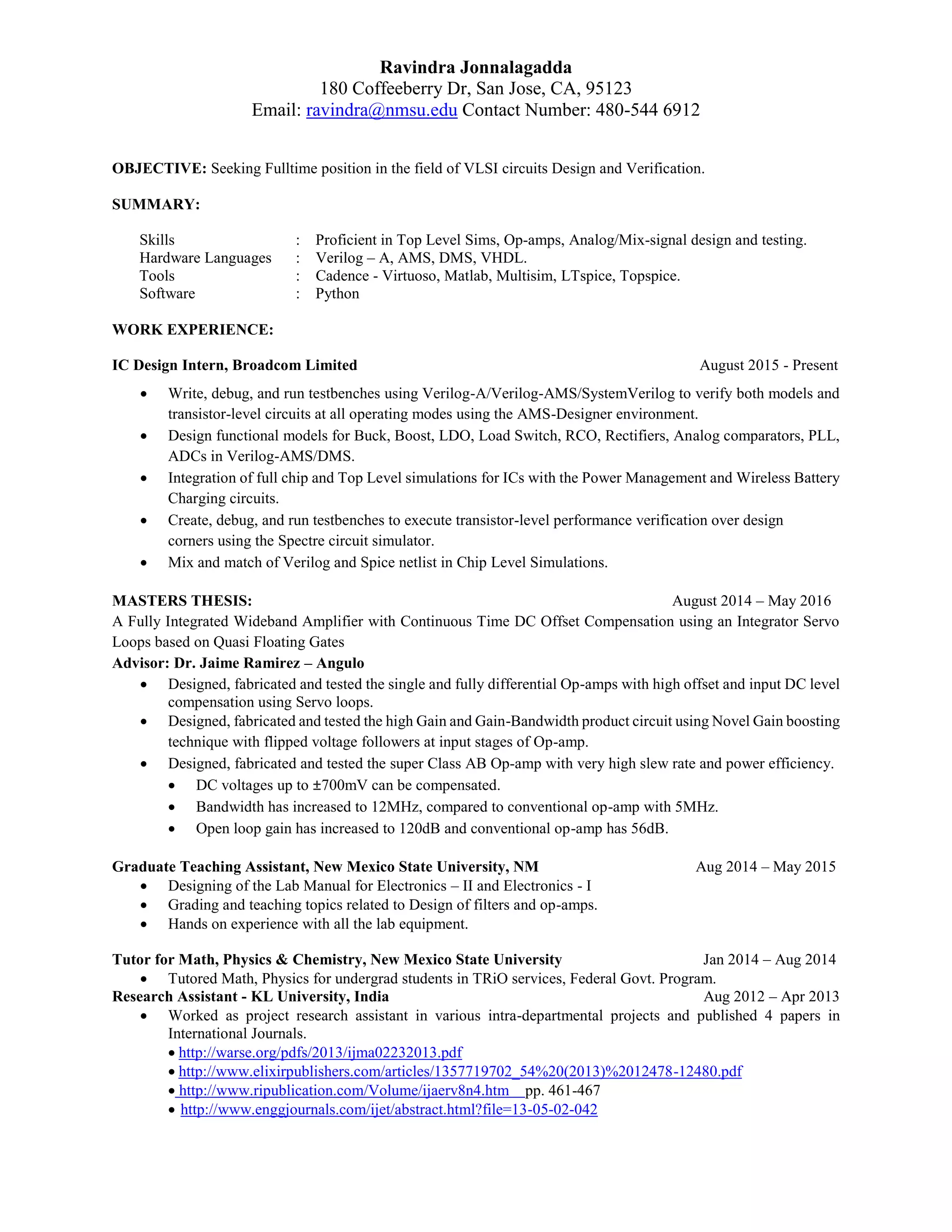
Ravindra Jonnalagadda
180 Coffeeberry Dr, San Jose, CA, 95123
Email: ravindra@nmsu.edu Contact Number: 480-544 6912
OBJECTIVE: Seeking Fulltime position in the field of VLSI circuits Design and Verification.
SUMMARY:
Skills : Proficient in Top Level Sims, Op-amps, Analog/Mix-signal design and testing.
Hardware Languages : Verilog – A, AMS, DMS, VHDL.
Tools : Cadence - Virtuoso, Matlab, Multisim, LTspice, Topspice.
Software : Python
WORK EXPERIENCE:
IC Design Intern, Broadcom Limited August 2015 - Present
ď‚· Write, debug, and run testbenches using Verilog-A/Verilog-AMS/SystemVerilog to verify both models and
transistor-level circuits at all operating modes using the AMS-Designer environment.
ď‚· Design functional models for Buck, Boost, LDO, Load Switch, RCO, Rectifiers, Analog comparators, PLL,
ADCs in Verilog-AMS/DMS.
ď‚· Integration of full chip and Top Level simulations for ICs with the Power Management and Wireless Battery
Charging circuits.
ď‚· Create, debug, and run testbenches to execute transistor-level performance verification over design
corners using the Spectre circuit simulator.
ď‚· Mix and match of Verilog and Spice netlist in Chip Level Simulations.
MASTERS THESIS: August 2014 – May 2016
A Fully Integrated Wideband Amplifier with Continuous Time DC Offset Compensation using an Integrator Servo
Loops based on Quasi Floating Gates
Advisor: Dr. Jaime Ramirez – Angulo
ď‚· Designed, fabricated and tested the single and fully differential Op-amps with high offset and input DC level
compensation using Servo loops.
ď‚· Designed, fabricated and tested the high Gain and Gain-Bandwidth product circuit using Novel Gain boosting
technique with flipped voltage followers at input stages of Op-amp.
ď‚· Designed, fabricated and tested the super Class AB Op-amp with very high slew rate and power efficiency.
 DC voltages up to ±700mV can be compensated.
ď‚· Bandwidth has increased to 12MHz, compared to conventional op-amp with 5MHz.
ď‚· Open loop gain has increased to 120dB and conventional op-amp has 56dB.
Graduate Teaching Assistant, New Mexico State University, NM Aug 2014 – May 2015
 Designing of the Lab Manual for Electronics – II and Electronics - I
ď‚· Grading and teaching topics related to Design of filters and op-amps.
ď‚· Hands on experience with all the lab equipment.
Tutor for Math, Physics & Chemistry, New Mexico State University Jan 2014 – Aug 2014
ď‚· Tutored Math, Physics for undergrad students in TRiO services, Federal Govt. Program.
Research Assistant - KL University, India Aug 2012 – Apr 2013
ď‚· Worked as project research assistant in various intra-departmental projects and published 4 papers in
International Journals.
ď‚· http://warse.org/pdfs/2013/ijma02232013.pdf
ď‚· http://www.elixirpublishers.com/articles/1357719702_54%20(2013)%2012478-12480.pdf
ď‚· http://www.ripublication.com/Volume/ijaerv8n4.htm pp. 461-467
ď‚· http://www.enggjournals.com/ijet/abstract.html?file=13-05-02-042
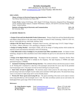
Ravindra Jonnalagadda
180 Coffeeberry Dr, San Jose, CA, 95123
Email: ravindra@nmsu.edu Contact Number: 480-544 6912
EDUCATION:
Master of Science in Electrical Engineering (Specialization: VLSI) GPA: 3.8
New Mexico State University, Las Cruces, NM May 2016
Course Work: Analog VLSI Design, ASIC, Digital VLSI Design, Electronics, Integrated Power Management
circuits, Random Signal Analysis, Computer Performance Analysis, A/D and D/A converters Design, VHDL,
Linear Control Systems.
Bachelor of Engineering in Electronics and Communications GPA: 3.8
KL University, India May 2013
ACADEMIC PROJECTS:
ď‚· Design of Gain and Gain-Bandwidth Product Enhancement - Design of high Gain and Gain Bandwidth product
with flipped voltage follower at the input stages of Op-amps in Cadence 0.18um Technology, VDD=0.9, VSS=-0.9,
(W/L)n =(10/0.4)uM (W/L)p =(40/0.4)uM and Ibias=30uA.
 Design of DC-DC Boost Converter – Designed a Boost converter, with Input range 2.8-4.2V, Output Voltage =
5V, Current = 100mA, Efficiency= 92%, operating at a frequency of 5MHz.
 Design of Vending Machine – Developed a VHDL code for the design of Vending machine which includes the
selection of items and transaction information with LCD interfacing.
 Fully Differential version of multiply by two precision Gain Offset cancellation circuit – In Cadence 0.18um
technology, designed an offset cancellation circuit which multiplies the gain by two and cancels the offset and Gain
errors.
 Design of the Digital Phased Locked Loop – The design of all the components – Frequency Divider, Phase
Detector, Charge Pump, Loop Filter to multiply by five frequency. The input frequency is 180MHz and output
generated Frequency is 900MHz.
ď‚· Automated Technology in Domicile Hostage Interface - The combined software and electronic project in which
an AC Waiting hall is interfaced to a data base of the passengers and provides the access only for the permitted
reserved passengers into it. The project uses the Go-Green ideology by saving the energy.
ď‚· Smart Solar cell and its applications - The electronic project which conserves the solar energy and used to
provide energy in the lack of sunlight. It can be widely used in automatic Traffic light systems. The natural heat energy
source is converted in to light energy and it’s an Eco-friendly project.
ď‚· Wireless DC Motor speed control using IR rays - The speed controlling of the motor can be made in wireless
terms using Infra-Red rays with wavelength 1um to 1 mm. The video surveillance systems can use such motors, the
handicapped finds a great usage of this for their movement.
References:
Dr. Jaime Ramirez-Angulo, Email: jairamir@nmsu.edu Phone: (575) 646 4406
Hassan Hanjani, Email: hassan.hanjani@broadcom.com Phone: (408) 922 8117
Dr. Wei Tang, Email: wtang@nmsu.edu Phone: (575) 646 5768

ravindra_job

  • 1.
    Ravindra Jonnalagadda 180 CoffeeberryDr, San Jose, CA, 95123 Email: ravindra@nmsu.edu Contact Number: 480-544 6912 OBJECTIVE: Seeking Fulltime position in the field of VLSI circuits Design and Verification. SUMMARY: Skills : Proficient in Top Level Sims, Op-amps, Analog/Mix-signal design and testing. Hardware Languages : Verilog – A, AMS, DMS, VHDL. Tools : Cadence - Virtuoso, Matlab, Multisim, LTspice, Topspice. Software : Python WORK EXPERIENCE: IC Design Intern, Broadcom Limited August 2015 - Present  Write, debug, and run testbenches using Verilog-A/Verilog-AMS/SystemVerilog to verify both models and transistor-level circuits at all operating modes using the AMS-Designer environment.  Design functional models for Buck, Boost, LDO, Load Switch, RCO, Rectifiers, Analog comparators, PLL, ADCs in Verilog-AMS/DMS.  Integration of full chip and Top Level simulations for ICs with the Power Management and Wireless Battery Charging circuits.  Create, debug, and run testbenches to execute transistor-level performance verification over design corners using the Spectre circuit simulator.  Mix and match of Verilog and Spice netlist in Chip Level Simulations. MASTERS THESIS: August 2014 – May 2016 A Fully Integrated Wideband Amplifier with Continuous Time DC Offset Compensation using an Integrator Servo Loops based on Quasi Floating Gates Advisor: Dr. Jaime Ramirez – Angulo  Designed, fabricated and tested the single and fully differential Op-amps with high offset and input DC level compensation using Servo loops.  Designed, fabricated and tested the high Gain and Gain-Bandwidth product circuit using Novel Gain boosting technique with flipped voltage followers at input stages of Op-amp.  Designed, fabricated and tested the super Class AB Op-amp with very high slew rate and power efficiency.  DC voltages up to ±700mV can be compensated.  Bandwidth has increased to 12MHz, compared to conventional op-amp with 5MHz.  Open loop gain has increased to 120dB and conventional op-amp has 56dB. Graduate Teaching Assistant, New Mexico State University, NM Aug 2014 – May 2015  Designing of the Lab Manual for Electronics – II and Electronics - I  Grading and teaching topics related to Design of filters and op-amps.  Hands on experience with all the lab equipment. Tutor for Math, Physics & Chemistry, New Mexico State University Jan 2014 – Aug 2014  Tutored Math, Physics for undergrad students in TRiO services, Federal Govt. Program. Research Assistant - KL University, India Aug 2012 – Apr 2013  Worked as project research assistant in various intra-departmental projects and published 4 papers in International Journals.  http://warse.org/pdfs/2013/ijma02232013.pdf  http://www.elixirpublishers.com/articles/1357719702_54%20(2013)%2012478-12480.pdf  http://www.ripublication.com/Volume/ijaerv8n4.htm pp. 461-467  http://www.enggjournals.com/ijet/abstract.html?file=13-05-02-042
  • 2.
    Ravindra Jonnalagadda 180 CoffeeberryDr, San Jose, CA, 95123 Email: ravindra@nmsu.edu Contact Number: 480-544 6912 EDUCATION: Master of Science in Electrical Engineering (Specialization: VLSI) GPA: 3.8 New Mexico State University, Las Cruces, NM May 2016 Course Work: Analog VLSI Design, ASIC, Digital VLSI Design, Electronics, Integrated Power Management circuits, Random Signal Analysis, Computer Performance Analysis, A/D and D/A converters Design, VHDL, Linear Control Systems. Bachelor of Engineering in Electronics and Communications GPA: 3.8 KL University, India May 2013 ACADEMIC PROJECTS:  Design of Gain and Gain-Bandwidth Product Enhancement - Design of high Gain and Gain Bandwidth product with flipped voltage follower at the input stages of Op-amps in Cadence 0.18um Technology, VDD=0.9, VSS=-0.9, (W/L)n =(10/0.4)uM (W/L)p =(40/0.4)uM and Ibias=30uA.  Design of DC-DC Boost Converter – Designed a Boost converter, with Input range 2.8-4.2V, Output Voltage = 5V, Current = 100mA, Efficiency= 92%, operating at a frequency of 5MHz.  Design of Vending Machine – Developed a VHDL code for the design of Vending machine which includes the selection of items and transaction information with LCD interfacing.  Fully Differential version of multiply by two precision Gain Offset cancellation circuit – In Cadence 0.18um technology, designed an offset cancellation circuit which multiplies the gain by two and cancels the offset and Gain errors.  Design of the Digital Phased Locked Loop – The design of all the components – Frequency Divider, Phase Detector, Charge Pump, Loop Filter to multiply by five frequency. The input frequency is 180MHz and output generated Frequency is 900MHz.  Automated Technology in Domicile Hostage Interface - The combined software and electronic project in which an AC Waiting hall is interfaced to a data base of the passengers and provides the access only for the permitted reserved passengers into it. The project uses the Go-Green ideology by saving the energy.  Smart Solar cell and its applications - The electronic project which conserves the solar energy and used to provide energy in the lack of sunlight. It can be widely used in automatic Traffic light systems. The natural heat energy source is converted in to light energy and it’s an Eco-friendly project.  Wireless DC Motor speed control using IR rays - The speed controlling of the motor can be made in wireless terms using Infra-Red rays with wavelength 1um to 1 mm. The video surveillance systems can use such motors, the handicapped finds a great usage of this for their movement. References: Dr. Jaime Ramirez-Angulo, Email: jairamir@nmsu.edu Phone: (575) 646 4406 Hassan Hanjani, Email: hassan.hanjani@broadcom.com Phone: (408) 922 8117 Dr. Wei Tang, Email: wtang@nmsu.edu Phone: (575) 646 5768