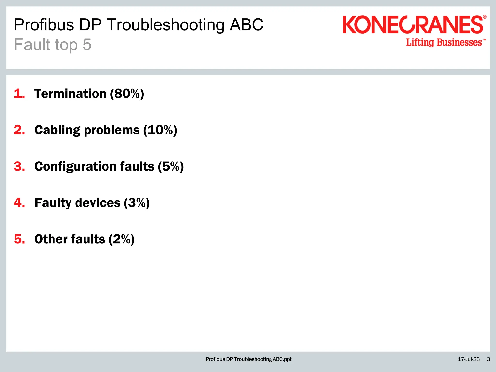
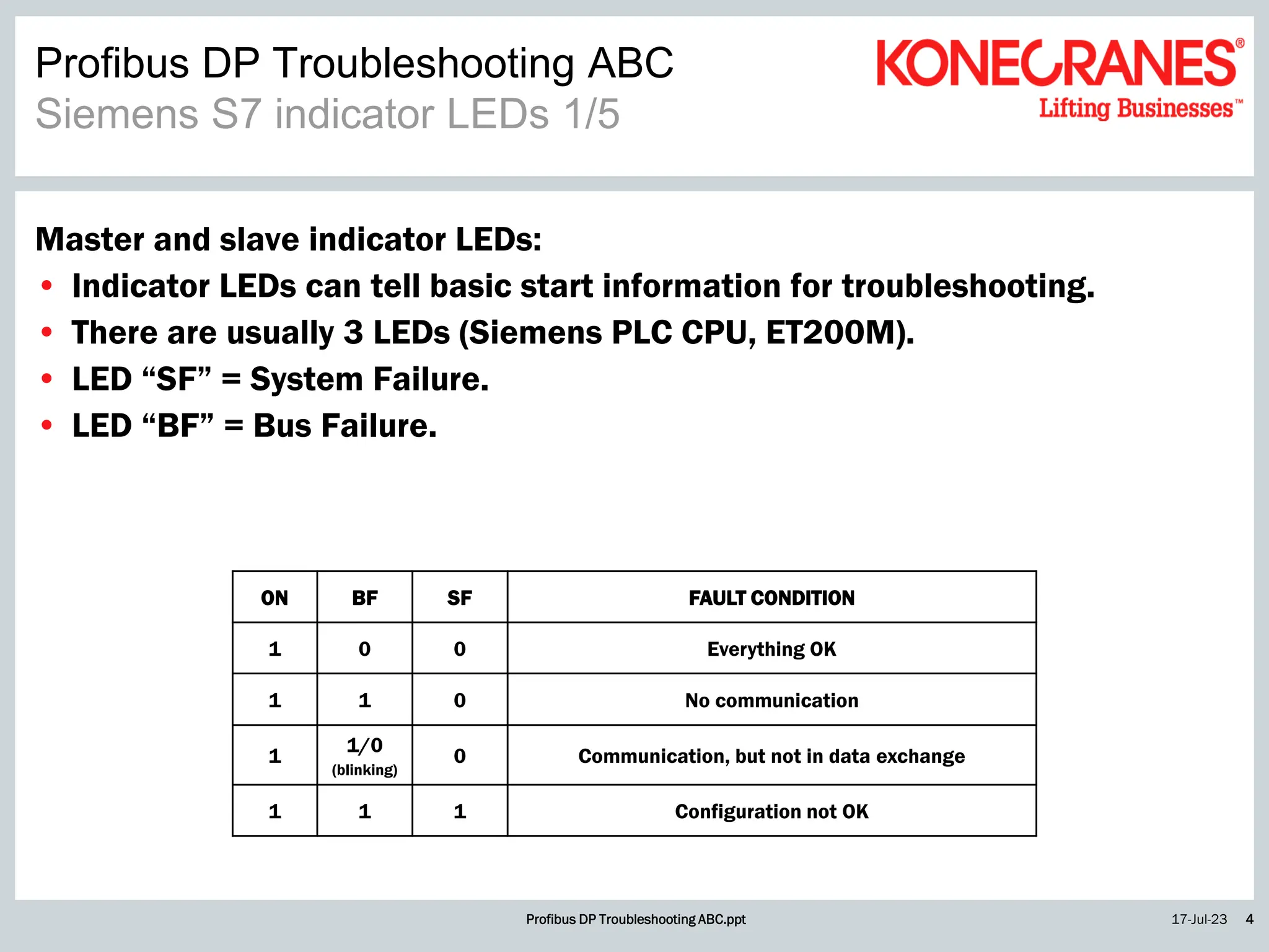
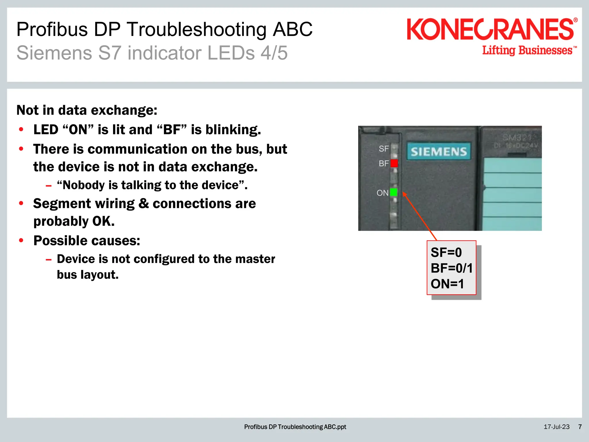
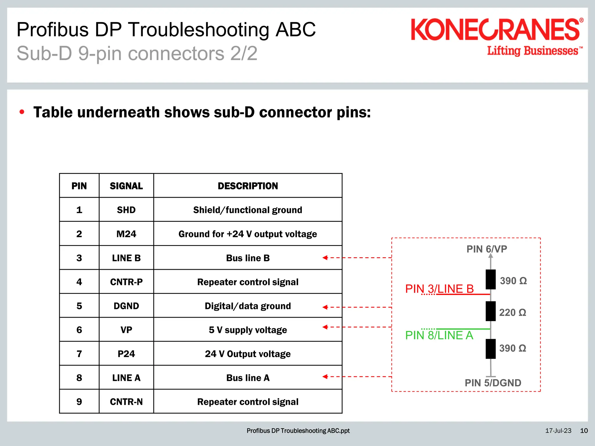
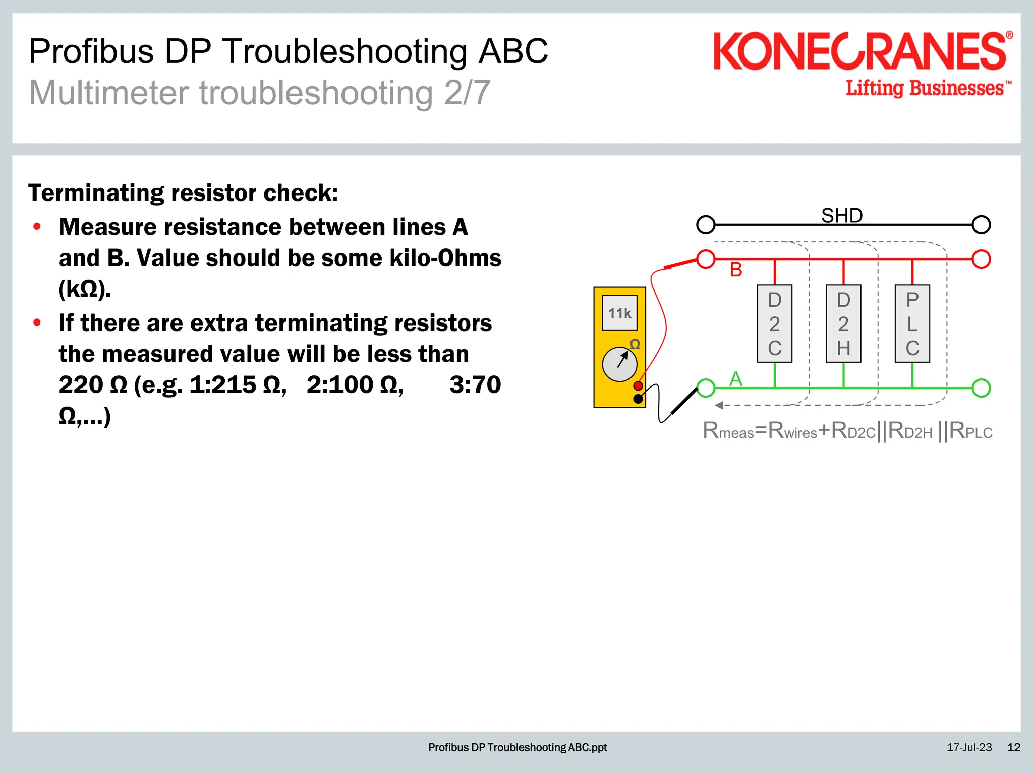
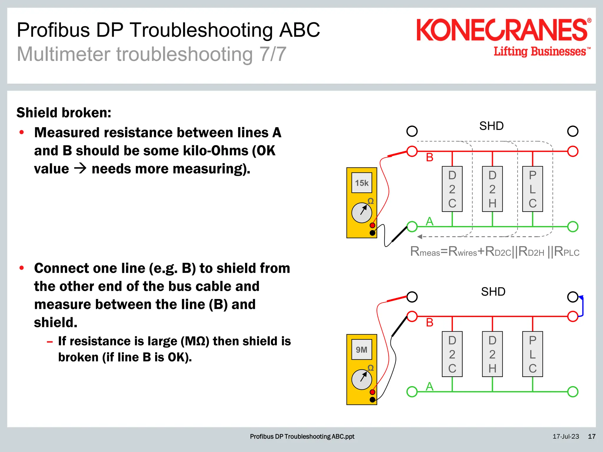
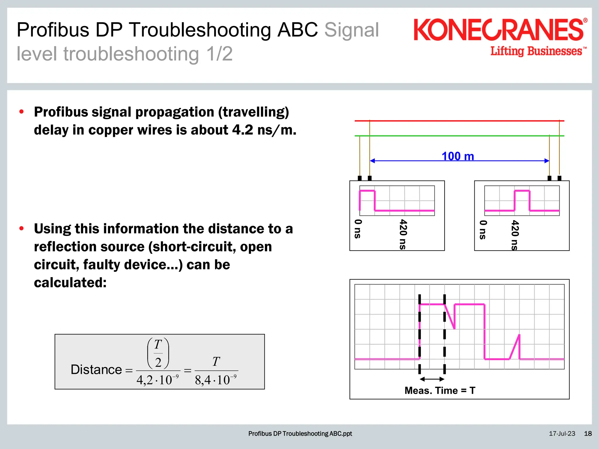
This document discusses designing combinational logic circuits using static complementary CMOS design. It explains how to construct static CMOS circuits for logic gates like NAND and NOR by using pull-up and pull-down networks of PMOS and NMOS transistors respectively. Issues related to pass-transistor design like noise margins and static power consumption are also covered. The document provides details on implementing various logic functions using pass-transistor logic and differential pass-transistor logic. It discusses solutions to overcome the disadvantages of pass-transistor logic like level restoration and use of multiple threshold transistors.
This document is a lab manual for analog and digital circuits experiments in the third semester of an electronics and communication engineering program. It contains 15 experiments, including experiments on common emitter, common collector, common source, Darlington, and differential amplifiers as well as various digital logic circuits like code converters, adders, multiplexers, and counters. For each analog experiment, the document provides the aim, apparatus required, circuit diagram, theoretical background, experimental procedure and expected results. It also contains an index listing the experiments and corresponding page numbers.
This document provides technical specifications, connections, diagrams and instructions for servicing a colour television. It includes:
1. Details on the chassis, models, dimensions, power requirements, reception capabilities, audio features and other technical specifications.
2. Instructions on safety, warnings and notes for servicing including using an isolation transformer and ensuring components are replaced with identical parts.
3. Overviews of the chassis layouts and diagrams of the boards, connections, wiring and components for the 15/17 inch and 23 inch television models. Block diagrams and test point mappings are provided.
This chapter discusses static CMOS circuits. It covers the goals of optimizing gate metrics like area, speed, energy and robustness. It discusses static CMOS logic families and high-performance circuit design techniques. Static CMOS circuits keep each gate output connected to either VDD or VSS at all times, unlike dynamic circuits which rely on temporary signal storage. The chapter explains how to construct static CMOS gates using pull-up and pull-down networks and discusses transistor sizing to optimize performance.
Parallel/flash ADCs use a voltage ladder and comparators to convert an analog input to a thermometer code. They can achieve sampling rates over 1GHz but require 2N-1 comparators. Interpolating and averaging ADCs reduce comparator count by interpolating between ladder voltages and averaging comparator outputs. Folding ADCs further reduce comparator count by mapping the input range onto a smaller set of subranges. Time-interleaved ADCs achieve high speeds by parallelizing conversions across multiple ADCs.
CMOS Analog IC design by Dr GS Javed - Refresher Course - Batch 1Javed G S, PhD
Topics covered in the course
1. DC Biasing of the circuits
2. Circuits for reference voltage and current generation
-Voltage Regulator
-BGR
-LDO
-V-to-I
3. Precision Current References
4. Opamp design for Analog to digital converters
- OTA
- Buffer
- Unity Feedback OTA
- Layout design strategies – 2stage opamp + CMFB
5. Sense and Return mechanisms in Feedback circuits
- Current and Voltage circuits
6. Sub-Threshold Conduction
- Low voltage Operation
7. ADC Design and Simulation
-Near Nyquist performance of Opamp for ADC Circuits
-Spectral Analysis and No. of FFT Points for simulation
-Simulation time for performance
-Resistors – their variation and Calibration
-Switch design for S/H
-CDAC
8. On-Chip Inductors
This document provides an overview of Ethernet technology, including its history and standards, hardware specifications, access methods, types of Ethernet, OSI and TCP/IP protocol layers, and connecting devices like switches, routers and firewalls. It also includes a hands-on example of network traffic between devices with different IP addresses, showing how switches, routers and firewalls direct the traffic between local and external networks.
This document discusses various types of analog-to-digital converters (ADCs). It describes integrating ADCs which work by integrating the input voltage over time and counting. Successive approximation ADCs work by successively refining the digital output until it approximates the input. Flash ADCs use many comparators in parallel to directly convert the input to a thermometer code. Other ADC types discussed include pipeline, interpolating, algorithmic, and time-interleaved ADCs. Issues in designing flash ADCs like input loading, resistor matching, and noise are also covered.
This document discusses different types of digital-to-analog converters (DACs), including parallel DACs, improved resolution parallel DACs, and serial DACs. It describes voltage scaling DACs which use a resistor ladder network and charge scaling DACs which use a capacitor array. It also examines integral nonlinearity (INL) and differential nonlinearity (DNL) for these DAC types and provides examples of calculating resolution based on component tolerances.
Designing Mixed Signal Systems with Noise Reduction Techniques in Mind focused on implementing noise reduction techniques when designing mixed signal systems. The presentation covered sources of noise such as devices, emissions, and traces; techniques to reduce noise like choosing lower noise devices, improving layout, and adding filtering; and applying these techniques across three design revisions to significantly reduce noise. Testing results showed noise levels drop from 44 code widths to just 1 after implementing various noise reduction strategies in a weight sensing application.
The document discusses different types of transistors including MOSFETs and BJTs. It then covers the basic construction and operation of MOSFETs and CMOS logic gates like inverters, NOR gates, and NAND gates. Decoder circuits are also summarized. The remainder discusses static hazards, output characteristics testing, and common logic interface levels.
The iot academy_embeddedsystems_training_circuitdesignpart3The IOT Academy
The document discusses circuit design abstraction levels and the circuit design process. It provides details on various circuit design concepts, including design abstraction levels, impedance matching, noise margins, propagation delay, reliability considerations, and fan-in and fan-out. The document also presents an example of designing a bias adjustment circuit for an LCD module and walks through specifying the problem, exploring design ideas, performing analysis, making assumptions, and developing a detailed circuit design.
This document discusses CMOS logic circuits. It begins by explaining that CMOS is the dominant technology for digital circuits due to its low power dissipation. It then discusses the structure and operation of the basic CMOS inverter circuit. Key points include that CMOS circuits use complementary NMOS and PMOS transistors to switch the output between power and ground with very low static power. The document also discusses parameters for characterizing logic circuits like propagation delay and noise margins. It describes how to synthesize more complex CMOS gates from their Boolean expressions by constructing pull-down and pull-up networks. Specific gates like NOR, NAND, and XOR are analyzed. Transistor sizing is also covered to ensure adequate driving capability.
This document summarizes testing of a one-stage pipelined analog-to-digital converter (ADC). It first describes the architecture of pipelined ADCs and the components of a single stage, including a sub-ADC comparator and multiplying digital-to-analog converter (MDAC). It then discusses fault models for circuit components and generates test inputs to detect faults. Specifically, it uses two test input voltages to generate output patterns that can detect faults like output stuck at supply voltages or capacitor opens/shorts through the digital outputs of each stage. Simulation parameters are provided and the document concludes by thanking the reader.
The document discusses various peripherals that can be interfaced with microcontrollers, including the 8255 Programmable Peripheral Interface (PPI), ADC0809 analog to digital converter, DAC0800 digital to analog converter, and serial communication standards like RS-232. It provides details on the architecture and interfacing of the 8255 PPI and describes how its ports are selected and programmed. It also provides interfacing diagrams and example programs for interfacing the 8255 with an 8051 microcontroller, as well as for interfacing the ADC0809 and DAC0800 for analog to digital and digital to analog conversion respectively. Finally, it discusses serial communication standards like RS-232, RS-485, RS-
The NCM provides a means of connecting Notifier fire alarm control products to the NOTI-FIRE-NET network. There are two types of NCMs: the NCM-W connects nodes with twisted-pair wire and supports NFPA Style 4 or 7 operation, while the NCM-F connects nodes with fiber-optic cable and its data transmission is immune to environmental noise. The document provides installation and wiring instructions for both models, as well as information on their diagnostic indicators and supplemental documentation.
This document discusses the design and operation of an all-digital phase locked loop (ADPLL). It covers topics such as the digitally controlled oscillator (DCO) core design, noise modeling in the ADPLL, tuning the ADPLL for GSM, impairments like capacitor mismatch and compensation techniques.
This document provides instructions for a lab experiment involving a 4-bit digital-to-analog converter (D/A converter) using an operational amplifier. Students are asked to perform transient analyses in Multisim with different resistor configurations for the D/A converter and observe the input and output voltages. They are to plot the timing diagrams and write the truth tables for the output voltage for each resistor configuration case. The goal is to understand the behavior of the D/A converter and verify the output voltage for different bit combinations.
The document discusses analog-to-digital and digital-to-analog converters. It covers key concepts like resolution, bandwidth, energy, sampling, quantization error, and signal-to-noise ratio. Common converter architectures are described, including parallel, R-2R ladder, weighted capacitor, and current-switched DACs as well as flash, pipelined, successive approximation, dual-slope, and sigma-delta ADCs. Tradeoffs between speed, accuracy, and chip area are also addressed.
The document provides specifications for the DS-37-16 Electric Encoder. It is a hollow shaft encoder that provides absolute position measurement with various output options. Key specifications include a resolution of 17 bits, static error of less than 25 mDeg, operational speed of 3,500 rpm, and operating temperature range of -55°C to +125°C. It has generous mounting tolerances and requires no bearings, making it reliable and suitable for demanding applications.
This document provides instructions for the control circuit of KEB COMBIVERT F5 frequency inverters. It describes the assignment of terminals on the control terminal strip X2A and how to connect the control circuit. It also outlines the operation of the optional operator interface used for parameter input and drive control.
The document discusses the programmable interface device 8155 and its applications. It describes the block diagram and address calculation of the 8155. It then discusses interfacing LEDs and generating square waves using the 8155 timer. It also covers the handshake and interrupt modes of the 8155 and interfacing an A/D converter using the handshake mode. The document provides code examples to initialize ports and display values on ports. It explains using the 8155 to read data from an A/D converter and display it on seven segment LEDs while recording the conversion time.
This document provides a summary of the DMS-40PC Series 41⁄2 Digit LED Display Digital Panel Voltmeters. Key points include:
- The voltmeters provide precision measurement in a compact package, with accuracy of ±2 counts or ±0.005% of full scale.
- Models have differential input voltage ranges of ±2V, ±20V, and ±200V. Additional features include a large LED display, single 5V supply, and optional BCD outputs.
- The epoxy-encapsulated package is rugged for harsh environments and temperatures from 0-50°C.
- Input impedance is a minimum of 800kΩ. Common mode rejection ratio
This document describes a dual 12-bit DAC chip. It contains two 12-bit DACs, on-chip voltage reference, output amplifiers, and reference buffer amplifiers. It can operate from a single or dual power supply. Key specifications include 12-bit resolution, differential nonlinearity of ±0.9 LSB max, output ranges of 0-5V, 0-10V, and ±5V. The chip comes in a 28-lead CQFP package and is screened using various reliability tests according to MIL-STD-883.
Clipper circuits were studied including series, parallel, and dual clipper configurations. Various clipper circuits were simulated using Multisim software and tested using hardware. Key aspects:
1) Series, parallel, and dual clipper circuits were designed to clip either the positive or negative portions of input signals.
2) Biased and unbiased clipper circuits were analyzed both in simulation and using hardware. External biasing was applied to parallel clipper circuits.
3) Input signals of 5V were clipped in various ways depending on the circuit configuration and applied biases. Output waveforms were observed on an oscilloscope.
4) Clipper circuits have applications in limiting signal amplitudes for applications like FM radio
This document discusses cabling for networking devices. It identifies the components needed to connect routers and switches for LAN and WAN connectivity. It explains Ethernet and WAN cabling standards as well as how to set up console connections. Cable types, connectors, and configurations for straight-through, crossover, and rollover are defined for Ethernet and serial WAN implementations. Visual diagrams are also provided to illustrate physical network topologies and device interfaces.
1. Delta-sigma ADCs use fully differential switched capacitor circuits for their analog parts. This improves dynamic range and cancels common mode signals and charge injection errors.
2. A 1.5V, 1mW, 98dB fourth-order delta-sigma modulator is discussed as an example. It uses a multi-stage pipelined architecture with four integrators.
3. Decimation and digital filtering are required after the analog delta-sigma modulation. Comb filters and FIR filters are commonly used to attenuate noise, bandlimit signals, and suppress out-of-band components during decimation and filtering.
1. The document discusses performance metrics and measurement techniques for analog-to-digital converters (ADCs). It provides high-level overviews of key ADC performance metrics like effective number of bits (ENOB), integral nonlinearity (INL), and differential nonlinearity (DNL).
2. Measurement techniques like the histogram method are explained, where a histogram of code bin occurrences is used to estimate parameters and characterize the ADC. Simple sine wave fitting using the outmost decision levels is presented as well.
3. An overview of ADC state-of-the-art is given, showing steady improvement in resolution over time but slower improvement in sampling rate. Progress in reducing power consumption and figures of merit has been more rapid.
Similar to Profibus DP Troubleshooting - Kone cranes Rev 1507.pdf (20)
Building a Raspberry Pi Robot with Dot NET 8, Blazor and SignalRPeter Gallagher
In this session delivered at NDC Oslo 2024, I talk about how you can control a 3D printed Robot Arm with a Raspberry Pi, .NET 8, Blazor and SignalR.
I also show how you can use a Unity app on an Meta Quest 3 to control the arm VR too.
You can find the GitHub repo and workshop instructions here;
https://bit.ly/dotnetrobotgithub
4. 17-Jul-23 4
Profibus DP Troubleshooting ABC.ppt
Profibus DP Troubleshooting ABC
Siemens S7 indicator LEDs 1/5
Master and slave indicator LEDs:
• Indicator LEDs can tell basic start information for troubleshooting.
• There are usually 3 LEDs (Siemens PLC CPU, ET200M).
• LED “SF” = System Failure.
• LED “BF” = Bus Failure.
ON BF SF FAULT CONDITION
1 0 0 Everything OK
1 1 0 No communication
1
1/0
(blinking)
0 Communication, but not in data exchange
1 1 1 Configuration not OK
5. 17-Jul-23 5
Profibus DP Troubleshooting ABC.ppt
SF
BF
ON
Profibus DP Troubleshooting ABC
Siemens S7 indicator LEDs 2/5
Everything OK:
• Only LED “ON” is lit.
• There are no problems with bus
communication.
• All slaves have correct parameters.
• System ready for operation.
SF=0
BF=0
ON=1
6. 17-Jul-23 6
Profibus DP Troubleshooting ABC.ppt
SF
BF
ON
Profibus DP Troubleshooting ABC
Siemens S7 indicator LEDs 3/5
No communication:
• LEDs “ON” and “BF” are lit.
• There are no valid messages detected
on the bus.
• Possible causes:
– Wiring problems (break, cross-
connection…)
– Master PLC is OFF
SF=0
BF=1
ON=1
7. 17-Jul-23 7
Profibus DP Troubleshooting ABC.ppt
SF
BF
ON
Profibus DP Troubleshooting ABC
Siemens S7 indicator LEDs 4/5
Not in data exchange:
• LED “ON” is lit and “BF” is blinking.
• There is communication on the bus, but
the device is not in data exchange.
– “Nobody is talking to the device”.
• Segment wiring & connections are
probably OK.
• Possible causes:
– Device is not configured to the master
bus layout.
SF=0
BF=0/1
ON=1
8. 17-Jul-23 8
Profibus DP Troubleshooting ABC.ppt
SF
BF
ON
Profibus DP Troubleshooting ABC
Siemens S7 indicator LEDs 5/5
Configuration not OK:
• LEDs “ON”, “SF” and “BF” are lit.
• Possible causes:
– System configuration is not correct.
– Local problem (configured bus devices
offline…)
SF=1
BF=1
ON=1
9. 17-Jul-23 9
Profibus DP Troubleshooting ABC.ppt
Profibus DP Troubleshooting ABC
Sub-D 9-pin connectors 1/2
• Usually two bus cables can be
connected into a sub-D connector:
– IN
– OUT
• When termination is switched ON line
OUT is disconnected.
– All devices in the bus after the
termination will be cut out of the active
bus.
OFF ON
OFF ON
T
10. 17-Jul-23 10
Profibus DP Troubleshooting ABC.ppt
Profibus DP Troubleshooting ABC
Sub-D 9-pin connectors 2/2
• Table underneath shows sub-D connector pins:
PIN SIGNAL DESCRIPTION
1 SHD Shield/functional ground
2 M24 Ground for +24 V output voltage
3 LINE B Bus line B
4 CNTR-P Repeater control signal
5 DGND Digital/data ground
6 VP 5 V supply voltage
7 P24 24 V Output voltage
8 LINE A Bus line A
9 CNTR-N Repeater control signal
PIN 5/DGND
PIN 6/VP
390 Ω
PIN 3/LINE B
PIN 8/LINE A
220 Ω
390 Ω
11. 17-Jul-23 11
Profibus DP Troubleshooting ABC.ppt
Profibus DP Troubleshooting ABC
Multimeter troubleshooting 1/7
• The resistance (measured with a multimeter) of each device connected in
parallel between the bus lines should be 30kΩ…220kΩ.
• Terminating resistors from both ends of the bus segment should be
disconnected before measurements.
• Before measuring draw a clear picture of the bus wiring and devices:
(T) T
LINE B
LINE A
220Ω
30kΩ…220kΩ
(each device)
220Ω
SHIELD
D
2
C
D
2
H
P
L
C
T T
12. 17-Jul-23 12
Profibus DP Troubleshooting ABC.ppt
Profibus DP Troubleshooting ABC
Multimeter troubleshooting 2/7
Terminating resistor check:
• Measure resistance between lines A
and B. Value should be some kilo-Ohms
(kΩ).
• If there are extra terminating resistors
the measured value will be less than
220 Ω (e.g. 1:215 Ω, 2:100 Ω, 3:70
Ω,…)
D
2
C
D
2
H
P
L
C
Rmeas=Rwires+RD2C||RD2H ||RPLC
11k
Ω
SHD
B
A
13. 17-Jul-23 13
Profibus DP Troubleshooting ABC.ppt
Profibus DP Troubleshooting ABC
Multimeter troubleshooting 3/7
Wires cross-connected:
• Measured resistance between lines A
and B should be some kilo-Ohms
(normally OK value needs more
measuring).
• Connect one line (e.g. line B) to shield
from the other end of the bus cable.
Measurement between the other line
(e.g. line A) and shield should give
some Ohms.
D
2
C
D
2
H
P
L
C
Rmeas=Rwires+RD2C||RD2H ||RPLC
SHD
B
A
11k
Ω
Rmeas=Rwire+RSHD
D
2
C
D
2
H
P
L
C
5.0
Ω
SHD
B
A
14. 17-Jul-23 14
Profibus DP Troubleshooting ABC.ppt
Profibus DP Troubleshooting ABC
Multimeter troubleshooting 4/7
Wire broken:
• Measured resistance between lines A
and B should be some kilo-Ohms
(normally OK value needs more
measuring).
• Connect one line (e.g. B) to shield from
the other end of the bus cable and
measure between the line (B) and
shield.
– If resistance is large (kΩ) the line (B) is
broken.
D
2
C
D
2
H
P
L
C
Rmeas=Rwires+RD2C||RD2H
SHD
B
A
15k
Ω
D
2
C
D
2
H
P
L
C
55k
Ω
SHD
B
A
Rmeas=Rwire+RD2C||RD2H+RPLC +RSHD
15. 17-Jul-23 15
Profibus DP Troubleshooting ABC.ppt
Profibus DP Troubleshooting ABC
Multimeter troubleshooting 5/7
Wire short-circuit:
• Measured resistance between lines A
and B should be some Ohms (wire
resistance in parallel with device
resistances).
• The place of short-circuit can be found
by using termination to cut out parts of
the bus.
– If termination is switched ON before
short-circuit measured value will be
about 220 Ω.
– If termination is switched ON after short-
circuit measured value will be some
Ohms.
D
2
C
D
2
H
P
L
C
Rmeas=Rwires+RD2C||RD2H ||RPLC
SHD
B
A
3.0
Ω
D
2
C
D
2
H
P
L
C
SHD
B
A
221
Ω
Rmeas=Rwires+RTerm||RD2C
T
16. 17-Jul-23 16
Profibus DP Troubleshooting ABC.ppt
Profibus DP Troubleshooting ABC
Multimeter troubleshooting 6/7
Line short-circuit to shield:
• Measured resistance between lines A
and B should be some kilo-Ohms (OK
value needs more measuring).
• Measured resistance between short
circuited lines (e.g. B and shield)
should be some Ohms.
D
2
C
D
2
H
P
L
C
Rmeas=Rwires+RD2C||RD2H ||RPLC
SHD
B
A
15k
Ω
D
2
C
D
2
H
P
L
C
SHD
B
A
1.4
Ω
Rmeas=Rwire +RSHD
17. 17-Jul-23 17
Profibus DP Troubleshooting ABC.ppt
Profibus DP Troubleshooting ABC
Multimeter troubleshooting 7/7
Shield broken:
• Measured resistance between lines A
and B should be some kilo-Ohms (OK
value needs more measuring).
• Connect one line (e.g. B) to shield from
the other end of the bus cable and
measure between the line (B) and
shield.
– If resistance is large (MΩ) then shield is
broken (if line B is OK).
D
2
C
D
2
H
P
L
C
Rmeas=Rwires+RD2C||RD2H ||RPLC
SHD
B
A
D
2
C
D
2
H
P
L
C
SHD
B
A
9M
Ω
15k
Ω
18. 17-Jul-23 18
Profibus DP Troubleshooting ABC.ppt
Profibus DP Troubleshooting ABC Signal
level troubleshooting 1/2
• Profibus signal propagation (travelling)
delay in copper wires is about 4.2 ns/m.
• Using this information the distance to a
reflection source (short-circuit, open
circuit, faulty device…) can be
calculated:
0
ns
420
ns
0
ns
420
ns
100 m
Meas. Time = T
9
9
10
4
,
8
10
2
,
4
2
T
T
Distance
19. 17-Jul-23 19
Profibus DP Troubleshooting ABC.ppt
Profibus DP Troubleshooting ABC Signal
level troubleshooting 2/2
• The measured signal form depends on both the measuring place and the
reflection place.
• When measuring from the same side of the problem as the signal source
the reflection can be seen.
SOURCE
T=250 ns
PROBLEM
BOUNDARY
30 m
Distance =T/(8,4*10-9)
=250* 10-9/(8,4*10-9)
=30 (m)
20. 17-Jul-23 20
Profibus DP Troubleshooting ABC.ppt
Profibus DP Troubleshooting ABC
Troubleshooting checklist 1/2
• Termination
– If communication problems arise, always check terminating resistors first.
– Termination should be turned on from both ends of every segment.
– Draw the bus topology in way that every segment can be easily seen or follow
the bus cable from one end to the other.
– Be careful with the sub-D connector terminating switch.
• Sub-D connectors:
– Often cabling problems are found inside sub-D connectors.
• Air gaps
– Air gaps between power lines and bus cables should be large enough (>20 cm).
– Air gaps between control signal lines and bus cables should be large enough
(>10 cm).
21. 17-Jul-23 21
Profibus DP Troubleshooting ABC.ppt
Profibus DP Troubleshooting ABC
Troubleshooting checklist 2/2
• Cabling rules
– Segment cable lengths should be according to Profibus standard (1500kbit/s
max 200m).
– Stub line lengths should be according to Profibus standard (1500kbit/s max
6,6m).
– 1 meter rule should be observed.
– Grounding should be correct.
• Masters and slaves should be configured correctly.
• All devices connected to the bus should be operating and undamaged.