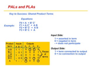
CS370 – Spring 2003
Programmable Logic Devices
       PALs/PLAs
PALs and PLAs

Pre-fabricated building block of many AND/OR gates (or NOR, NAND)
"Personalized" by making or breaking connections among the gates


   Programmable Array Block Diagram for Sum of Products Form


               Inputs


          Dense array of                      Dense array of
           AND gates         Product            OR gates
                              terms


                                                  Outputs
PALs and PLAs
    Key to Success: Shared Product Terms

             Equations
            F0 = A + B' C'
Example:    F1 = A C' + A B
            F2 = B' C' + A B
            F3 = B' C + A

                                       Input Side:
                                          1 = asserted in term
                                          0 = negated in term
 Product Inputs     Outputs               - = does not participate
  term   A B C    F0 F1 F2 F3
   AB    1 1 -     0 1 1 0            Output Side:
   BC    - 0 1     0 0 0 1      Reuse    1 = term connected to output
                                  of     0 = no connection to output
   AC    1 - 0     0 1 0 0
                                terms
   BC    - 0 0     1 0 1 0
    A    1 - -     1 0 0 1
PALs and PLAs
Example Continued         All possible connections are available
                                   before programming
         A   B   C


                     F0        F1     F2       F3
PALs and PLAs
    Example Continued
            A   B   C

                              Unwanted connections are "blown"

                               AB

                                /BC

                               A /C

                                /B /C

                                A


Note: some array structures
work by making connections
 rather than breaking them      F0      F1            F3
                                               F2
PALs and PLAs
Alternative representation for high fan-in structures


                                        Short-hand notation
                                      so that all the wires need
                                            not be drawn!


  A B   C D

                                AB
                                AB
                                         Notation for implementing
                                CD           F0 = A B + A' B'
                                             F1 = C D' + C' D
                                CD


                AB+AB CD + CD
PALs and PLAs
                                 A   B   C

Design Example                                                           ABC

                                                                         A

                                                                         B

                                                                         C
 Multiple functions of A, B, C                                           A

                                                                         B
   F1 = A B C
                                                                         C

   F2 = A + B + C                                                        ABC

                                                                         ABC
   F3 = A B C
                                                                         ABC

   F4 = A + B + C                                                        ABC

                                                                         ABC
   F5 = A xor B xor C
                                                                         ABC
   F6 = A xnor B xnor C                                                  ABC


                                             F1   F2   F3   F4 F5   F6
PALs and PLAs
 Difference between Programmable Array Logic (PAL) and
     Programmable Logic Array (PLA):

 PAL concept -- implemented by Monolithic Memories
   constrained topology of the OR Array – I.e., the OR
 array cannot be fully programmed.


                                   A given column of the OR array
                                   has access to only a subset of
                                     the possible product terms


 PLA concept generalized topologies in AND and OR planes
PALs and PLAs
     Design Example: BCD to Gray Code Converter

Truth Table   A   B   C   D   W   X   Y   Z                                        K-maps
              0   0   0   0   0   0   0   0
              0   0   0   1   0   0   0   1       AB
                                                                          A
                                                                                            AB
                                                                                                                    A
              0   0   1   0   0   0   1   1   CD       00   01       11       10        CD       00   01       11       10
              0   0   1   1   0   0   1   0
                                                  00    0    0        X       1             00    0    1        X       0
              0   1   0   0   0   1   1   0
              0   1   0   1   1   1   1   0
                                                  01    0    1        X       1             01    0    1        X       0
              0   1   1   0   1   0   1   0
                                                                                    D                                        D
              0   1   1   1   1   0   1   1             0    1        X       X                   0    0        X       X
                                                  11                                        11
              1   0   0   0   1   0   0   1   C                                         C
              1   0   0   1   1   0   0   0       10    0    1        X       X             10    0    0        X       X
              1   0   1   0   X   X   X   X
              1   0   1   1   X   X   X   X                      B                                         B
              1   1   0   0   X   X   X   X                 K-map for W                               K-map for X
              1   1   0   1   X   X   X   X
              1   1   1   0   X   X   X   X                               A                                         A
              1   1   1   1   X   X   X   X       AB                                        AB
                                              CD       00   01       11       10        CD       00   01       11       10

                                                  00    0    1        X       0             00    0    0        X       1
Minimized Functions:
                                                  01    0    1        X       0             01    1    0        X       0
W=A+BD+BC                                         11    1    1        X       X
                                                                                    D
                                                                                            11    0    1        X       X
                                                                                                                             D

X = B C'                                      C                                         C
Y=B+C                                             10    1    1        X       X             10    1    0        X       X

Z = A'B'C'D + B C D + A D' + B' C D'                             B                                         B
                                                            K-map for Y                               K-map for Z
PALs and PLAs                     A B C D

                                                           A
                                                           BD
 Programmed PAL:                                           BC

                                                           0

                                                           BC

                                                           0

                                                           0

                                                           0

                                                           B
                                                           C

                                                           0

                                                           0

                                                           ABCD

                                                           BCD
                                                           AD

                                                           BCD


4 product terms per each OR gate             W X   Y   Z
PALs and PLAs
Code Converter Discrete Gate Implementation

                A                                      A
A   1
                                                        B
                                                                 4
                                                        C
B                                                        D
            2                3       W
D
                                                  B
                                                  C       3
B           2                                     D
C                                                                              4 4   Z
                                                  A
                                                          5
B                                    D       1     D
                       2
                       2         1       X       B
C       1
                                                  C       3
                C                               D


                                                   1: 7404 hex inverters
                       2             Y
B       1                                        2,5: 7400 quad 2-input NAND
                B                                 3: 7410 tri 3-input NAND
                                                   4: 7420 dual 4-input NAND


                     4 SSI Packages vs. 1 PLA/PAL Package!
PALs and PLAs
    Example: Magnitude Comparator                                                 A   B   C D


                            A                                        A                                          ABCD
    AB                                       AB
CD       00   01       11       10       CD       00   01       11       10                                     ABCD
    00    1    0        0       0            00    0    1        1       1
                                                                                                                ABCD
    01    0    1        0       0            01    1    0        1       1
                                     D                                        D
                                                                                                                ABCD
    11    0    0        1       0            11    1    1        0       1
C                                        C
                                                                                                                AC
    10    0    0        0       1            10    1    1        1       0
                                                                                                                AC
                   B                                        B
                                                                                                                BD
              K-map for EQ                             K-map for NE
                                                                                                                BD
                            A                                        A
    AB                                       AB                                                                 ABD
CD       00   01       11       10       CD       00   01       11       10
    00    0    0        0       0            00    0    1        1       1
                                                                                                                BCD

                                                                                                                ABC
    01    1    0        0       0            01    0    0        1       1
                                     D                                        D                                 BCD
    11    1    1        0       1            11    0    0        0       0
C                                        C
    10    1    1        0       0            10    0    0        1       0


                   B                                        B
                                                                                                EQ NE LT   GT
              K-map for LT                             K-map for GT

Pla

  • 1.
    CS370 – Spring2003 Programmable Logic Devices PALs/PLAs
  • 2.
    PALs and PLAs Pre-fabricatedbuilding block of many AND/OR gates (or NOR, NAND) "Personalized" by making or breaking connections among the gates Programmable Array Block Diagram for Sum of Products Form Inputs Dense array of Dense array of AND gates Product OR gates terms Outputs
  • 3.
    PALs and PLAs Key to Success: Shared Product Terms Equations F0 = A + B' C' Example: F1 = A C' + A B F2 = B' C' + A B F3 = B' C + A Input Side: 1 = asserted in term 0 = negated in term Product Inputs Outputs - = does not participate term A B C F0 F1 F2 F3 AB 1 1 - 0 1 1 0 Output Side: BC - 0 1 0 0 0 1 Reuse 1 = term connected to output of 0 = no connection to output AC 1 - 0 0 1 0 0 terms BC - 0 0 1 0 1 0 A 1 - - 1 0 0 1
  • 4.
    PALs and PLAs ExampleContinued All possible connections are available before programming A B C F0 F1 F2 F3
  • 5.
    PALs and PLAs Example Continued A B C Unwanted connections are "blown" AB /BC A /C /B /C A Note: some array structures work by making connections rather than breaking them F0 F1 F3 F2
  • 6.
    PALs and PLAs Alternativerepresentation for high fan-in structures Short-hand notation so that all the wires need not be drawn! A B C D AB AB Notation for implementing CD F0 = A B + A' B' F1 = C D' + C' D CD AB+AB CD + CD
  • 7.
    PALs and PLAs A B C Design Example ABC A B C Multiple functions of A, B, C A B F1 = A B C C F2 = A + B + C ABC ABC F3 = A B C ABC F4 = A + B + C ABC ABC F5 = A xor B xor C ABC F6 = A xnor B xnor C ABC F1 F2 F3 F4 F5 F6
  • 8.
    PALs and PLAs Difference between Programmable Array Logic (PAL) and Programmable Logic Array (PLA): PAL concept -- implemented by Monolithic Memories constrained topology of the OR Array – I.e., the OR array cannot be fully programmed. A given column of the OR array has access to only a subset of the possible product terms PLA concept generalized topologies in AND and OR planes
  • 9.
    PALs and PLAs Design Example: BCD to Gray Code Converter Truth Table A B C D W X Y Z K-maps 0 0 0 0 0 0 0 0 0 0 0 1 0 0 0 1 AB A AB A 0 0 1 0 0 0 1 1 CD 00 01 11 10 CD 00 01 11 10 0 0 1 1 0 0 1 0 00 0 0 X 1 00 0 1 X 0 0 1 0 0 0 1 1 0 0 1 0 1 1 1 1 0 01 0 1 X 1 01 0 1 X 0 0 1 1 0 1 0 1 0 D D 0 1 1 1 1 0 1 1 0 1 X X 0 0 X X 11 11 1 0 0 0 1 0 0 1 C C 1 0 0 1 1 0 0 0 10 0 1 X X 10 0 0 X X 1 0 1 0 X X X X 1 0 1 1 X X X X B B 1 1 0 0 X X X X K-map for W K-map for X 1 1 0 1 X X X X 1 1 1 0 X X X X A A 1 1 1 1 X X X X AB AB CD 00 01 11 10 CD 00 01 11 10 00 0 1 X 0 00 0 0 X 1 Minimized Functions: 01 0 1 X 0 01 1 0 X 0 W=A+BD+BC 11 1 1 X X D 11 0 1 X X D X = B C' C C Y=B+C 10 1 1 X X 10 1 0 X X Z = A'B'C'D + B C D + A D' + B' C D' B B K-map for Y K-map for Z
  • 10.
    PALs and PLAs A B C D A BD Programmed PAL: BC 0 BC 0 0 0 B C 0 0 ABCD BCD AD BCD 4 product terms per each OR gate W X Y Z
  • 11.
    PALs and PLAs CodeConverter Discrete Gate Implementation A A A 1 B 4 C B D 2 3 W D B C 3 B 2 D C 4 4 Z A 5 B D 1 D 2 2 1 X B C 1 C 3 C D 1: 7404 hex inverters 2 Y B 1 2,5: 7400 quad 2-input NAND B 3: 7410 tri 3-input NAND 4: 7420 dual 4-input NAND 4 SSI Packages vs. 1 PLA/PAL Package!
  • 12.
    PALs and PLAs Example: Magnitude Comparator A B C D A A ABCD AB AB CD 00 01 11 10 CD 00 01 11 10 ABCD 00 1 0 0 0 00 0 1 1 1 ABCD 01 0 1 0 0 01 1 0 1 1 D D ABCD 11 0 0 1 0 11 1 1 0 1 C C AC 10 0 0 0 1 10 1 1 1 0 AC B B BD K-map for EQ K-map for NE BD A A AB AB ABD CD 00 01 11 10 CD 00 01 11 10 00 0 0 0 0 00 0 1 1 1 BCD ABC 01 1 0 0 0 01 0 0 1 1 D D BCD 11 1 1 0 1 11 0 0 0 0 C C 10 1 1 0 0 10 0 0 1 0 B B EQ NE LT GT K-map for LT K-map for GT