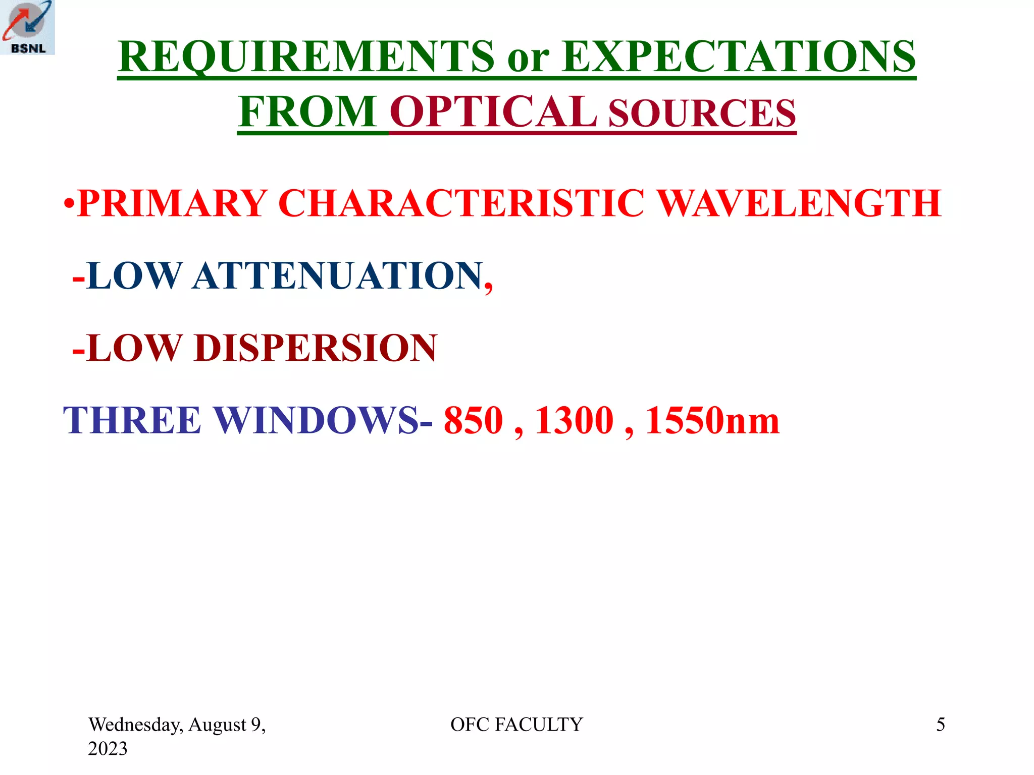
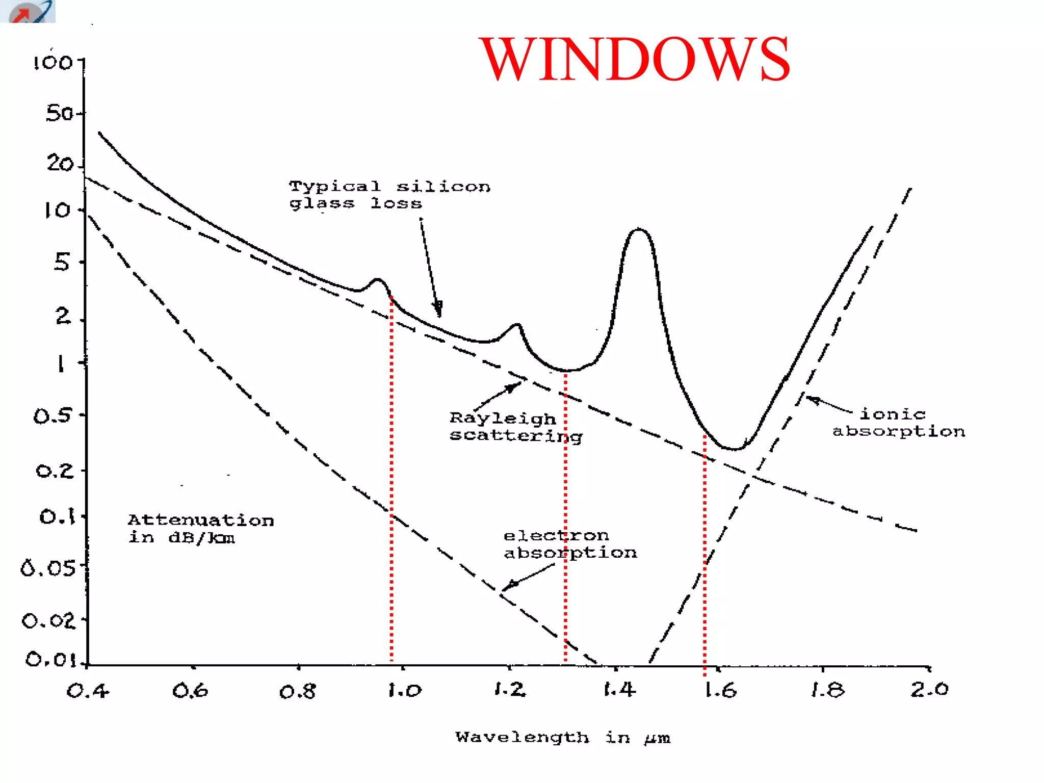
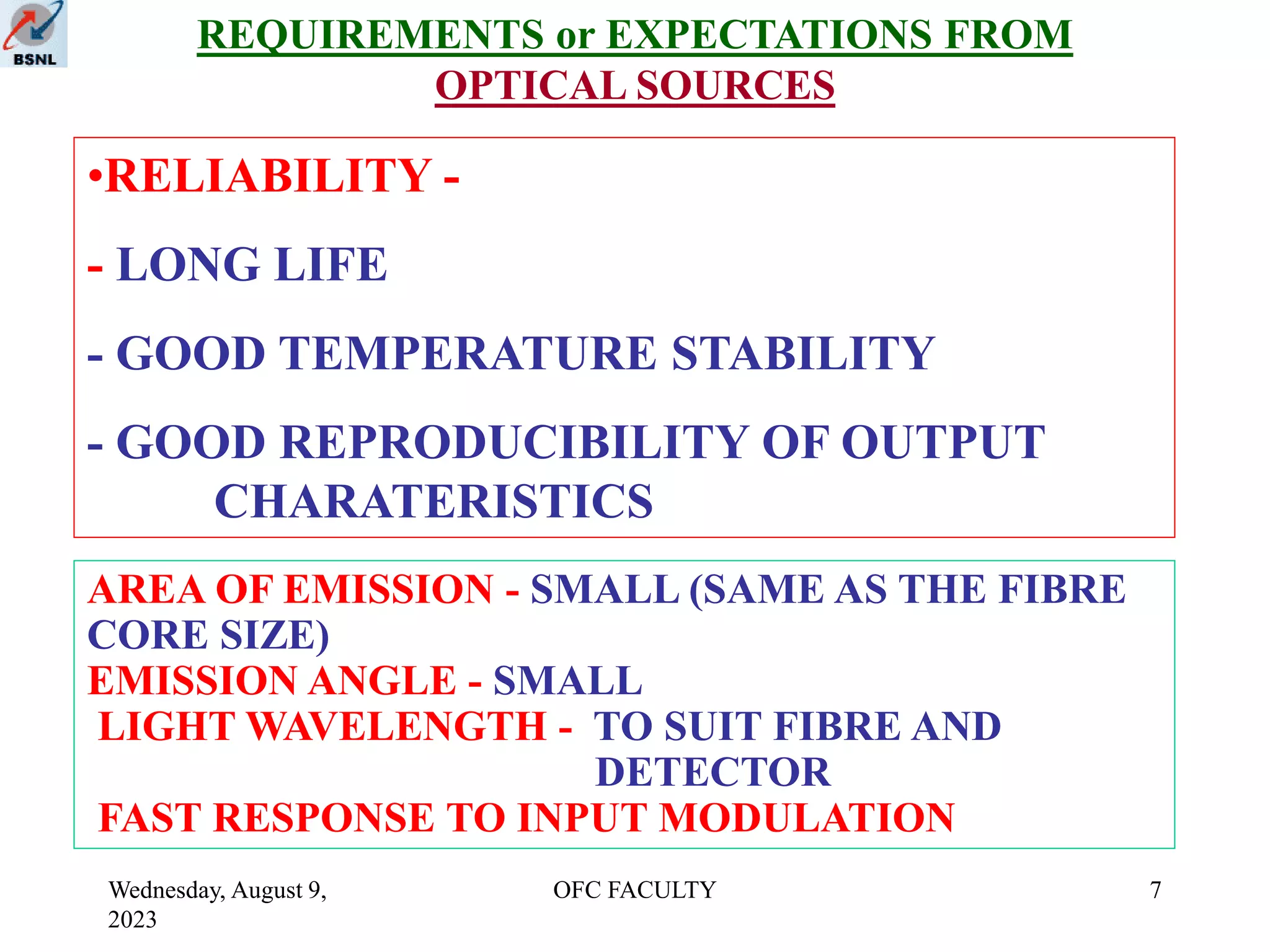
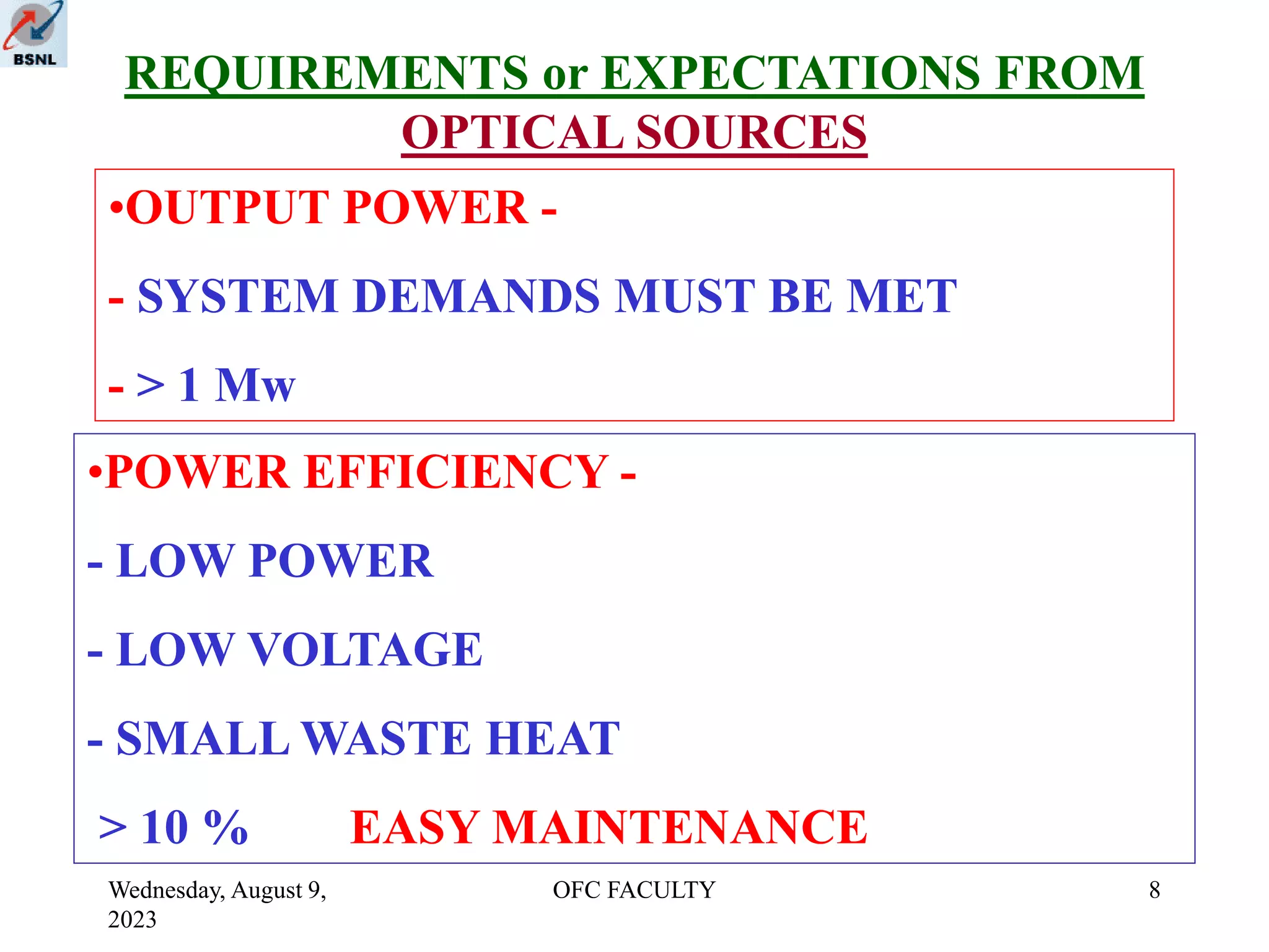
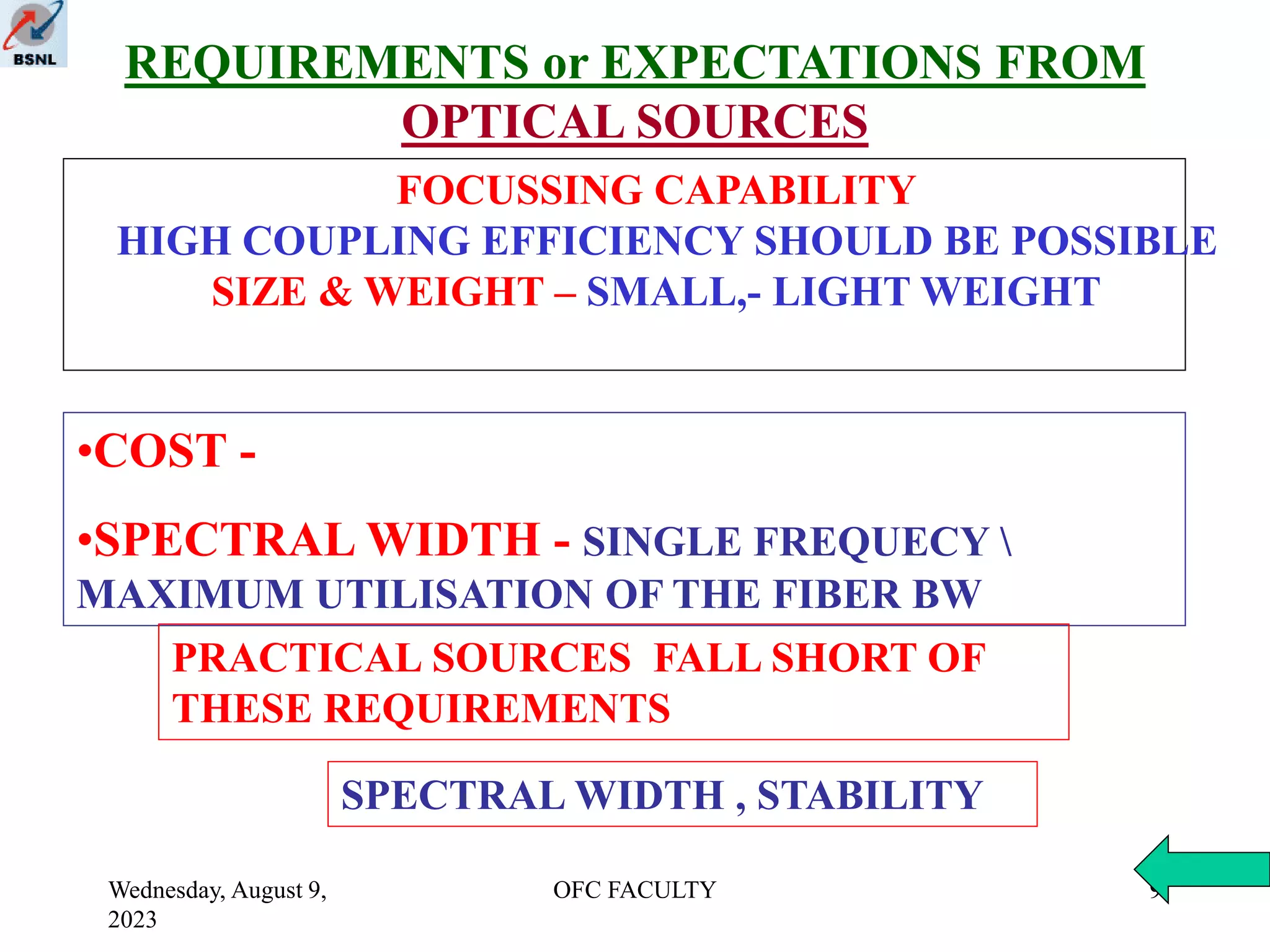
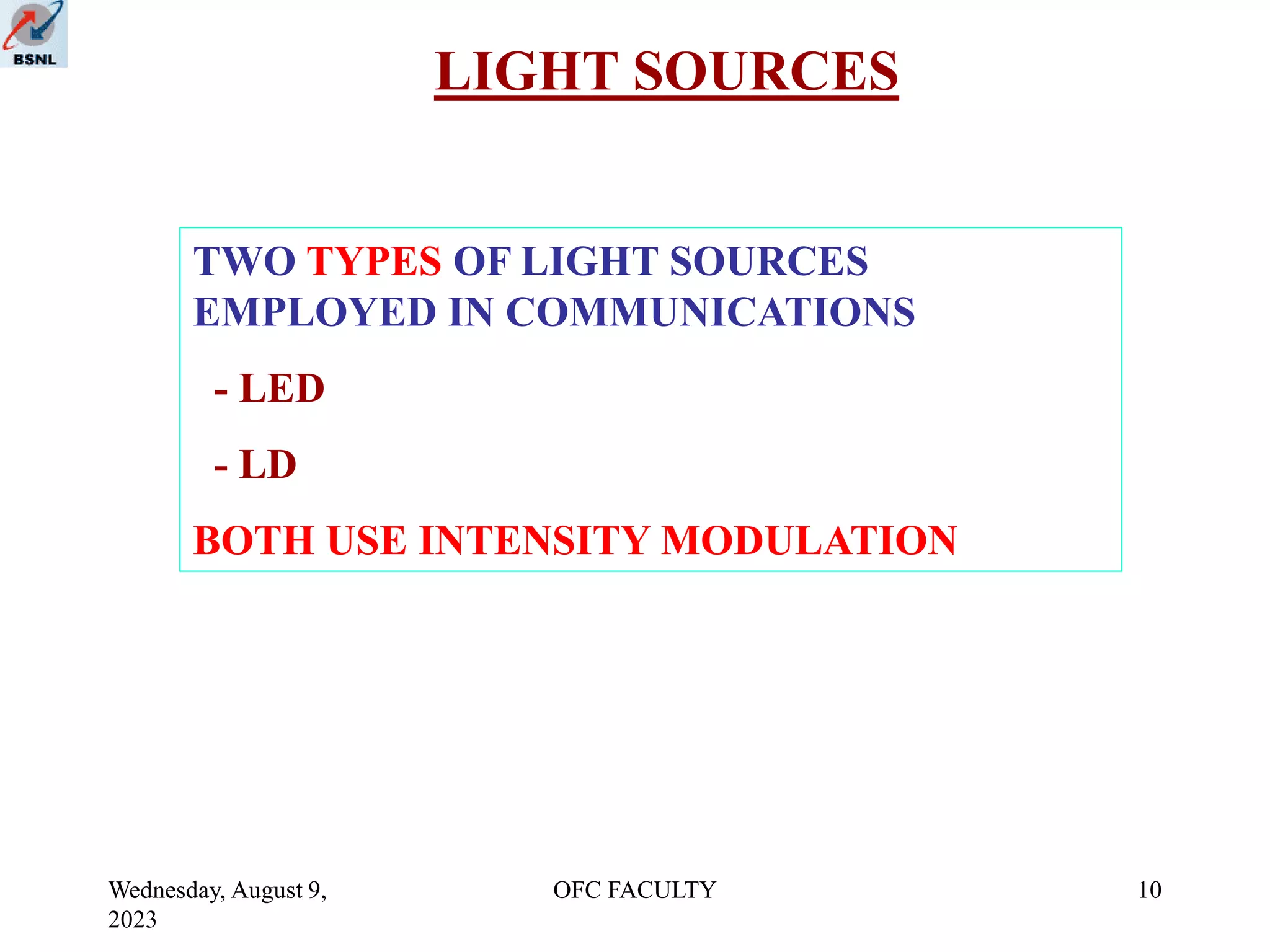
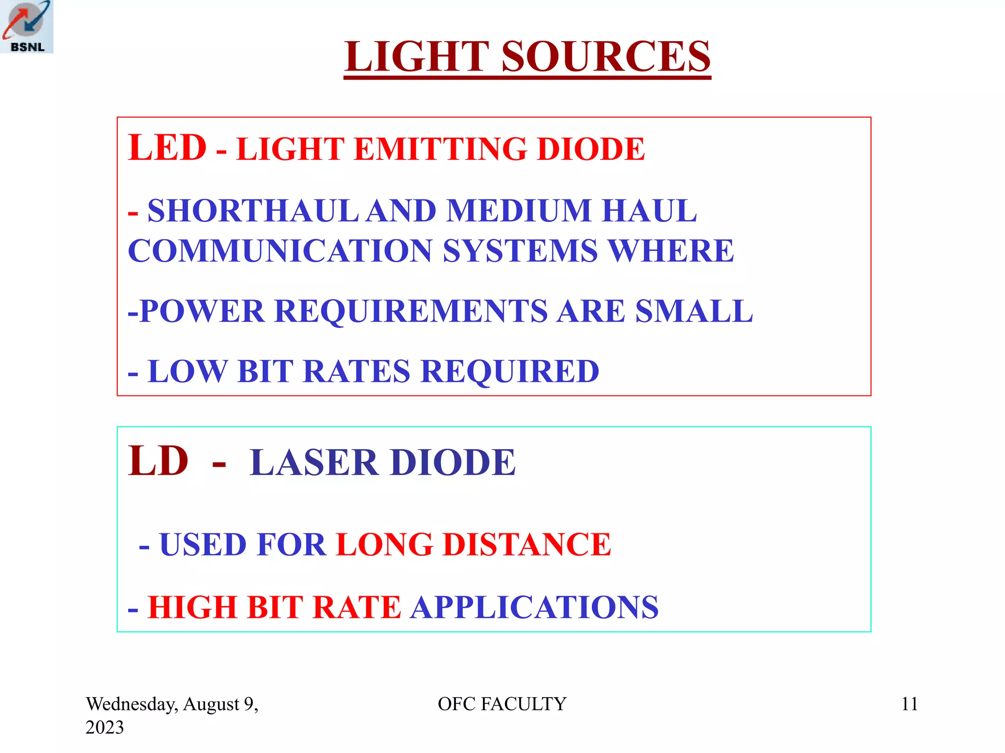
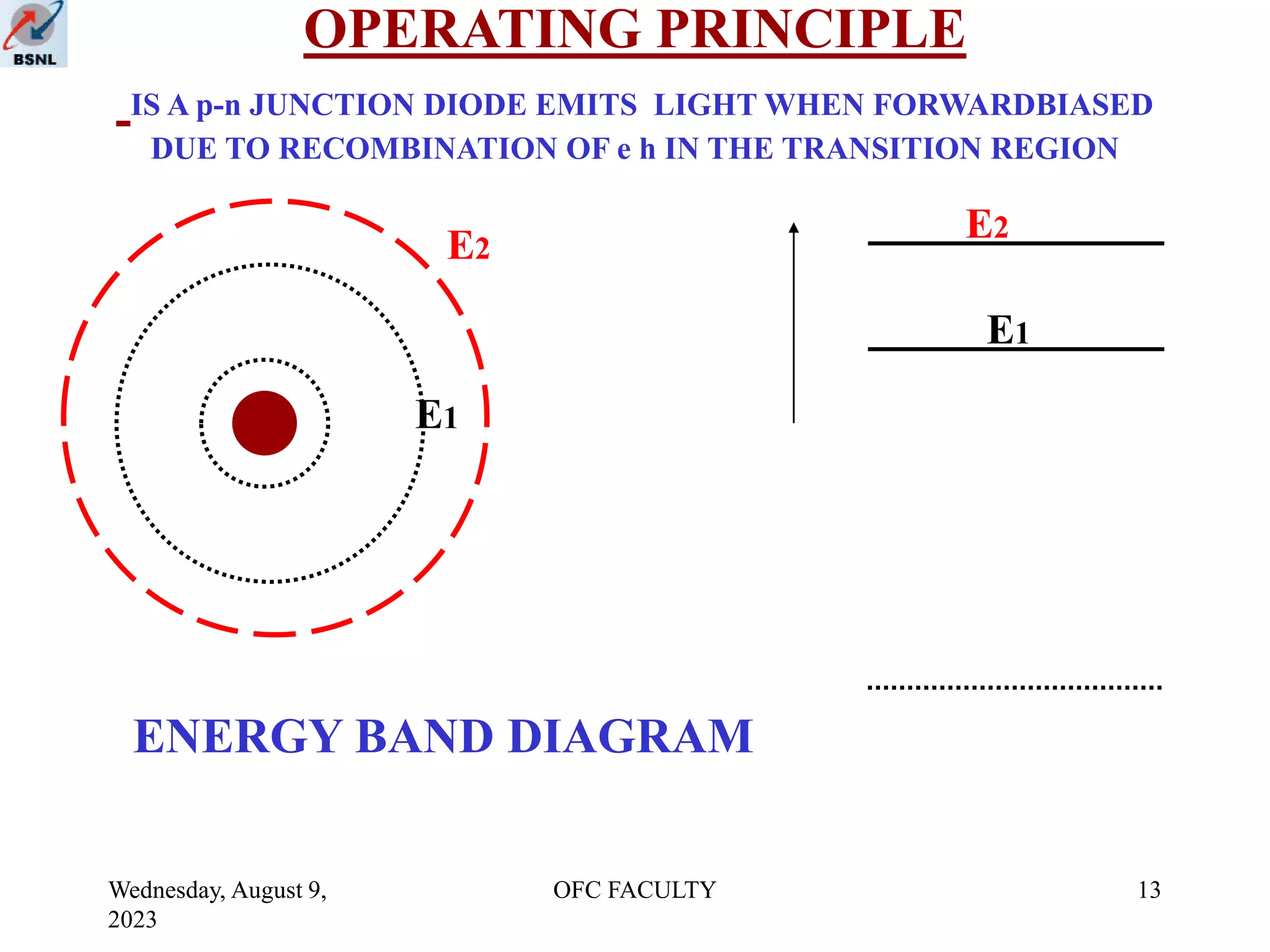
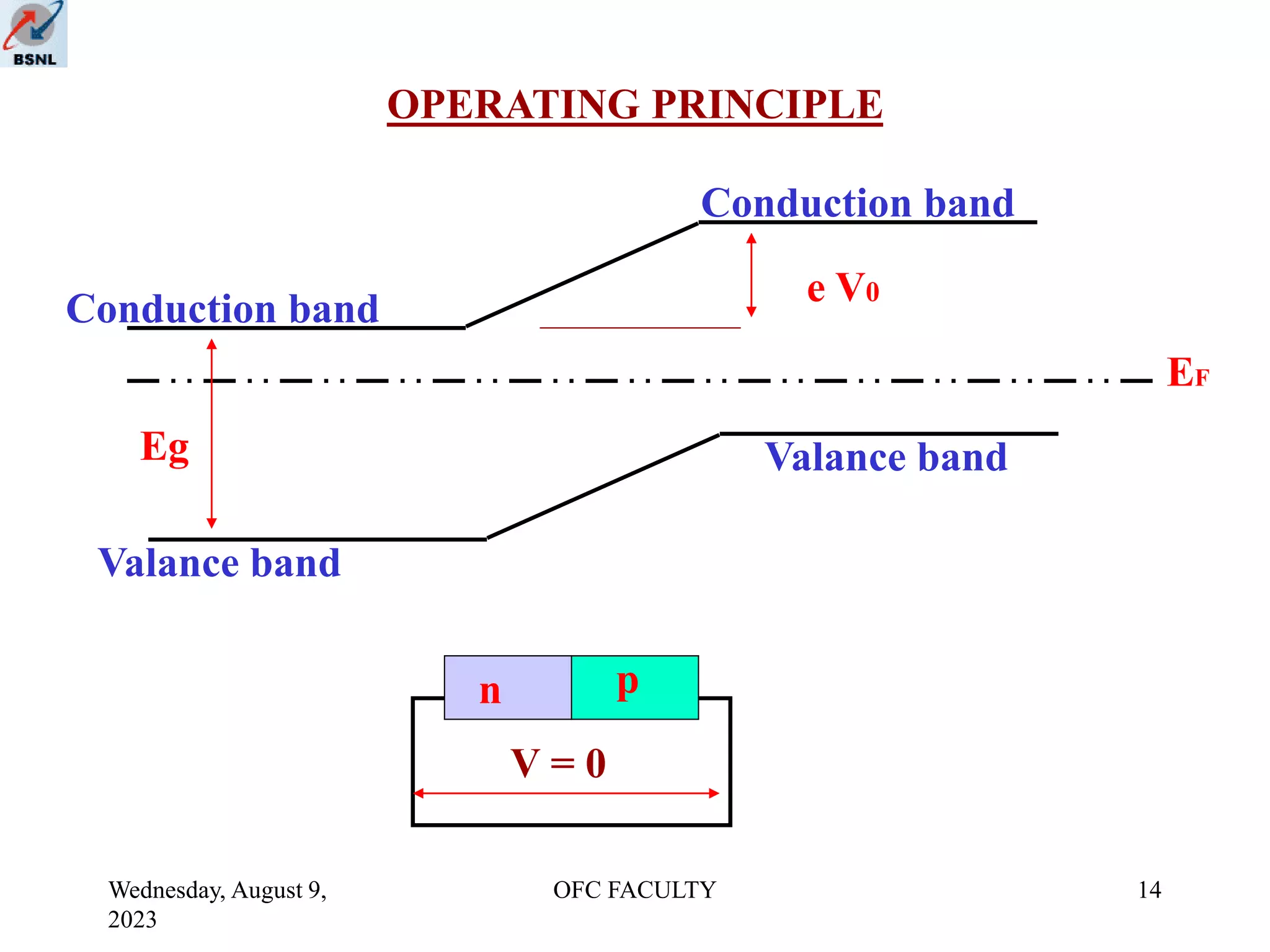
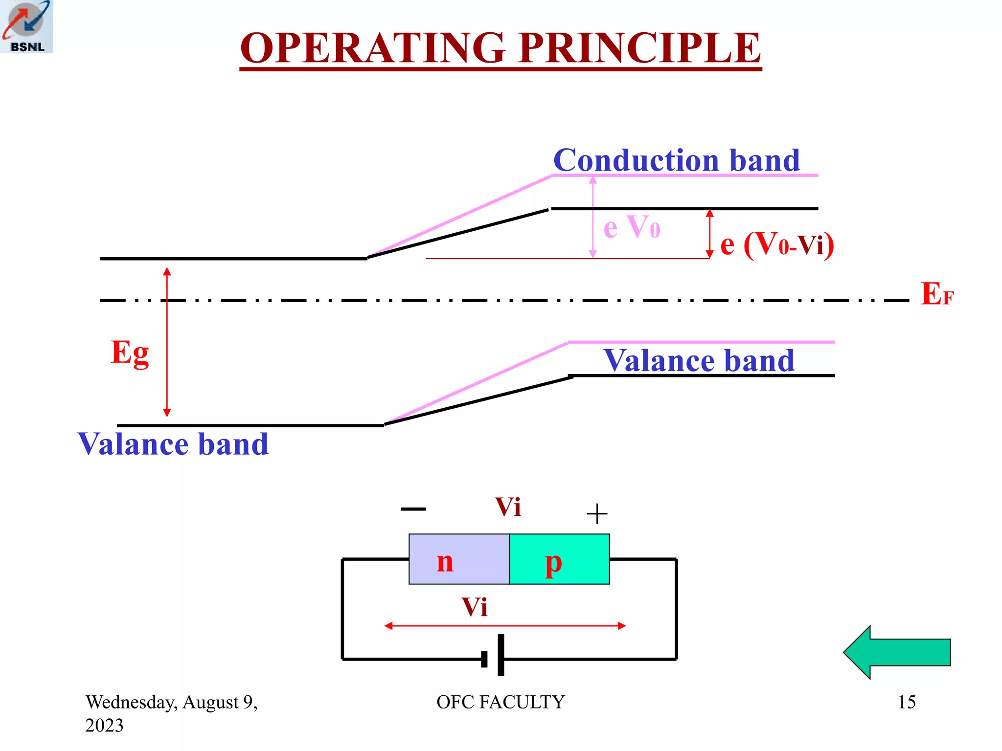
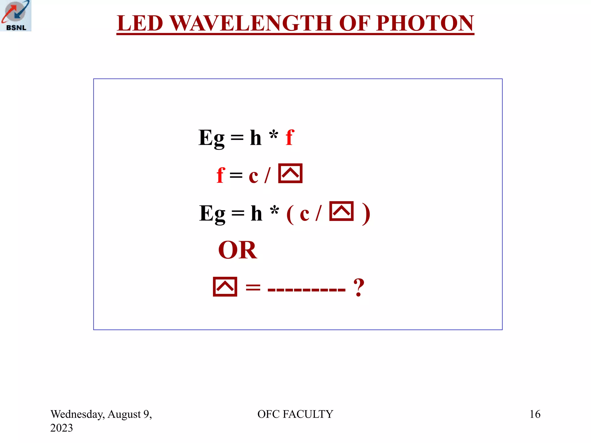
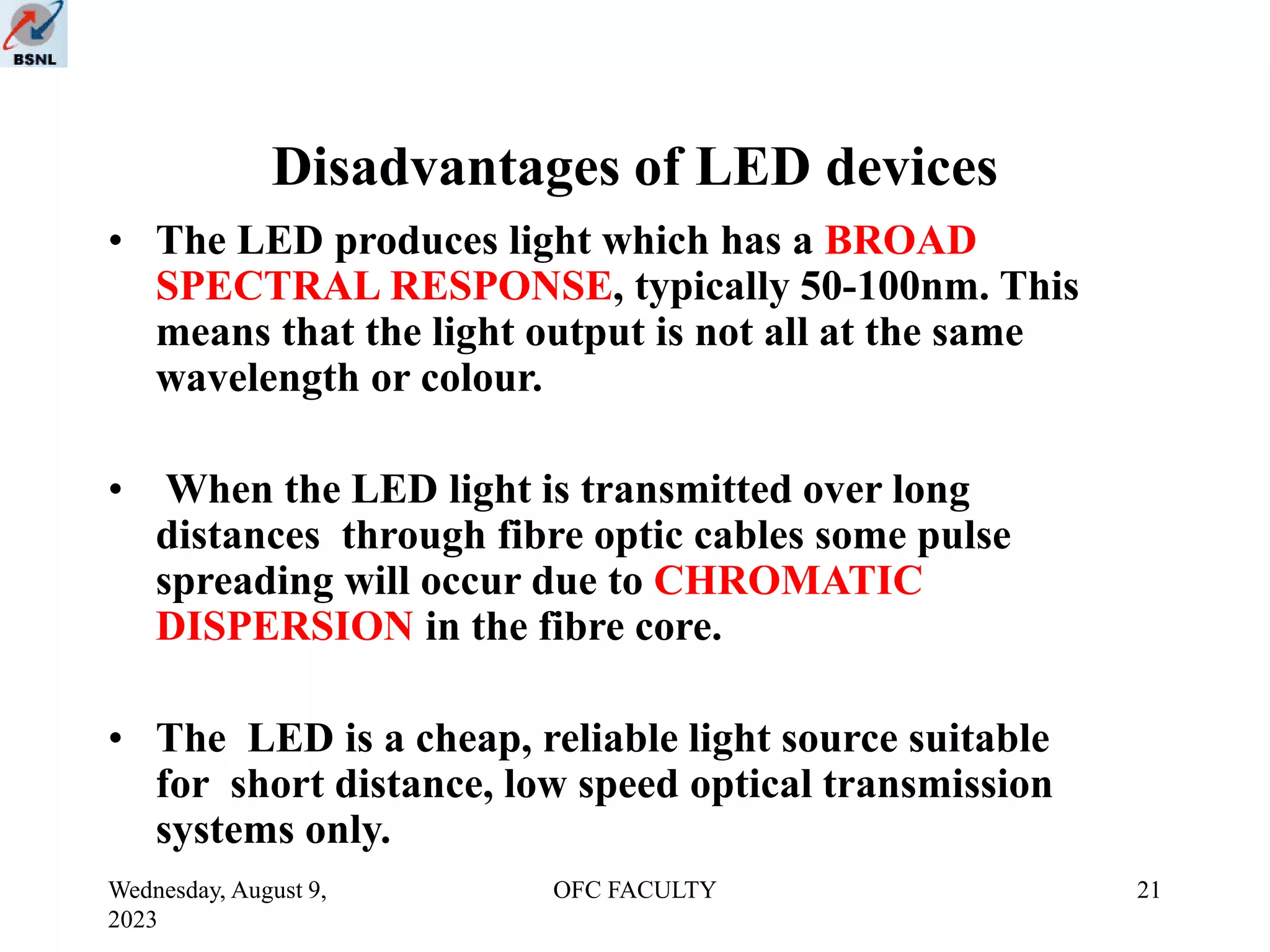
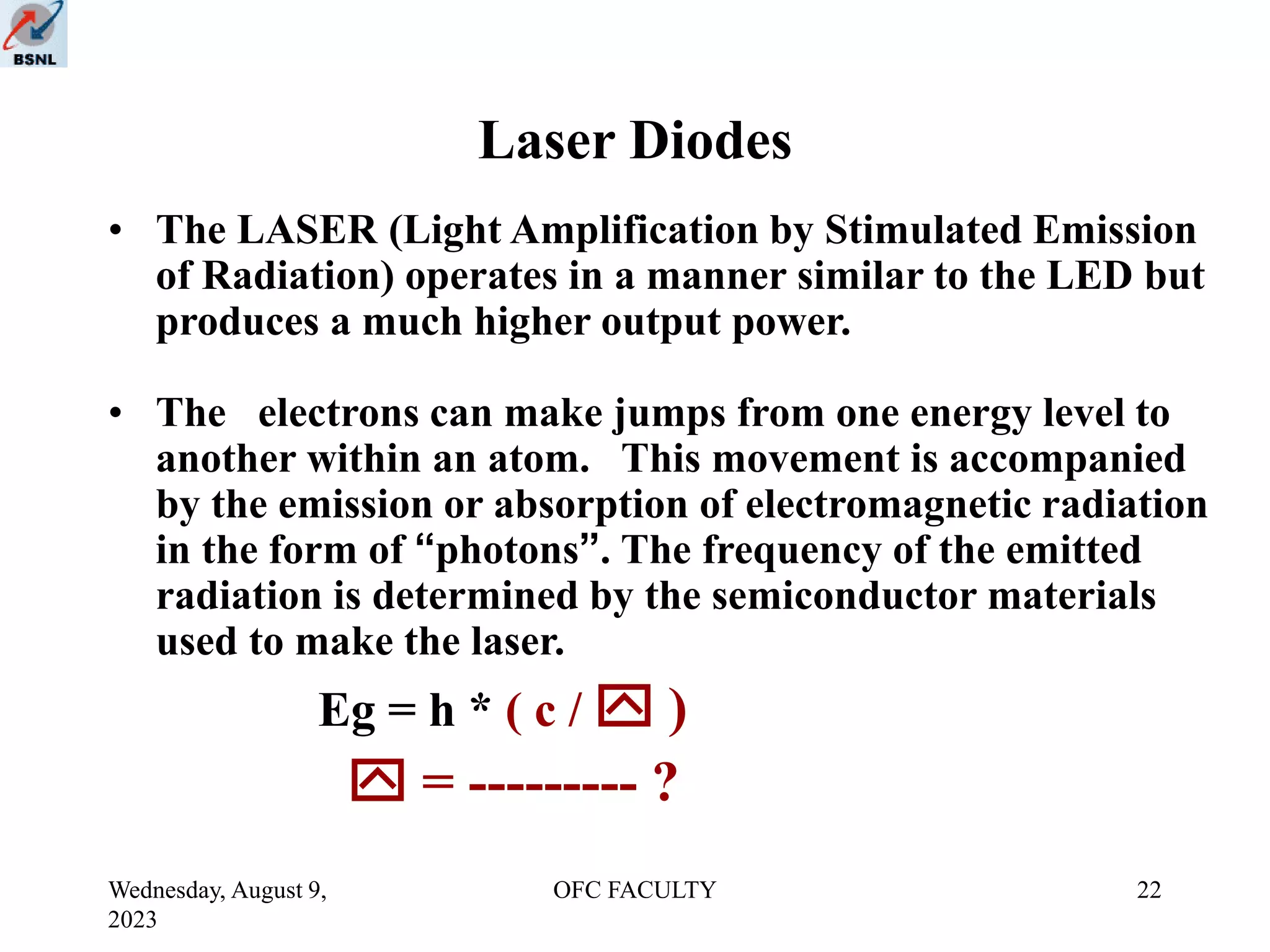
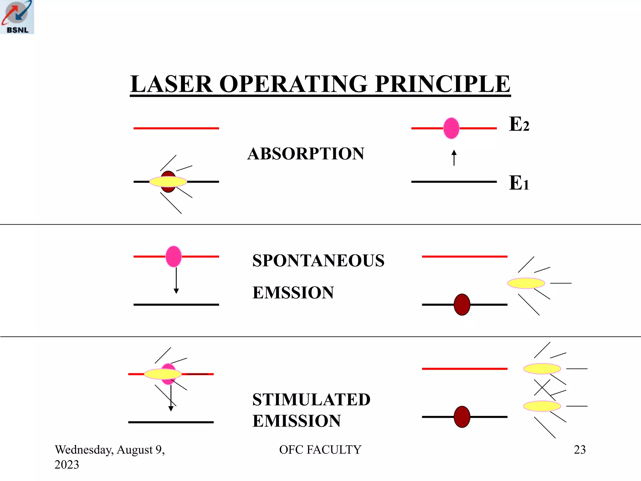
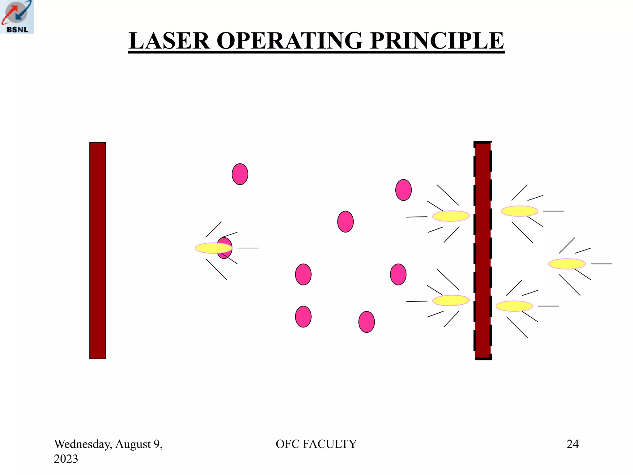
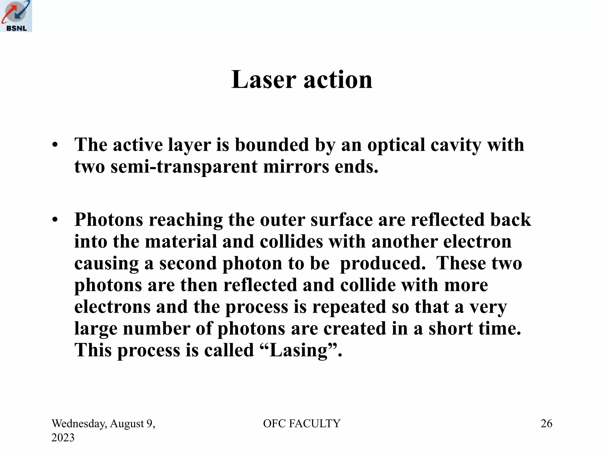
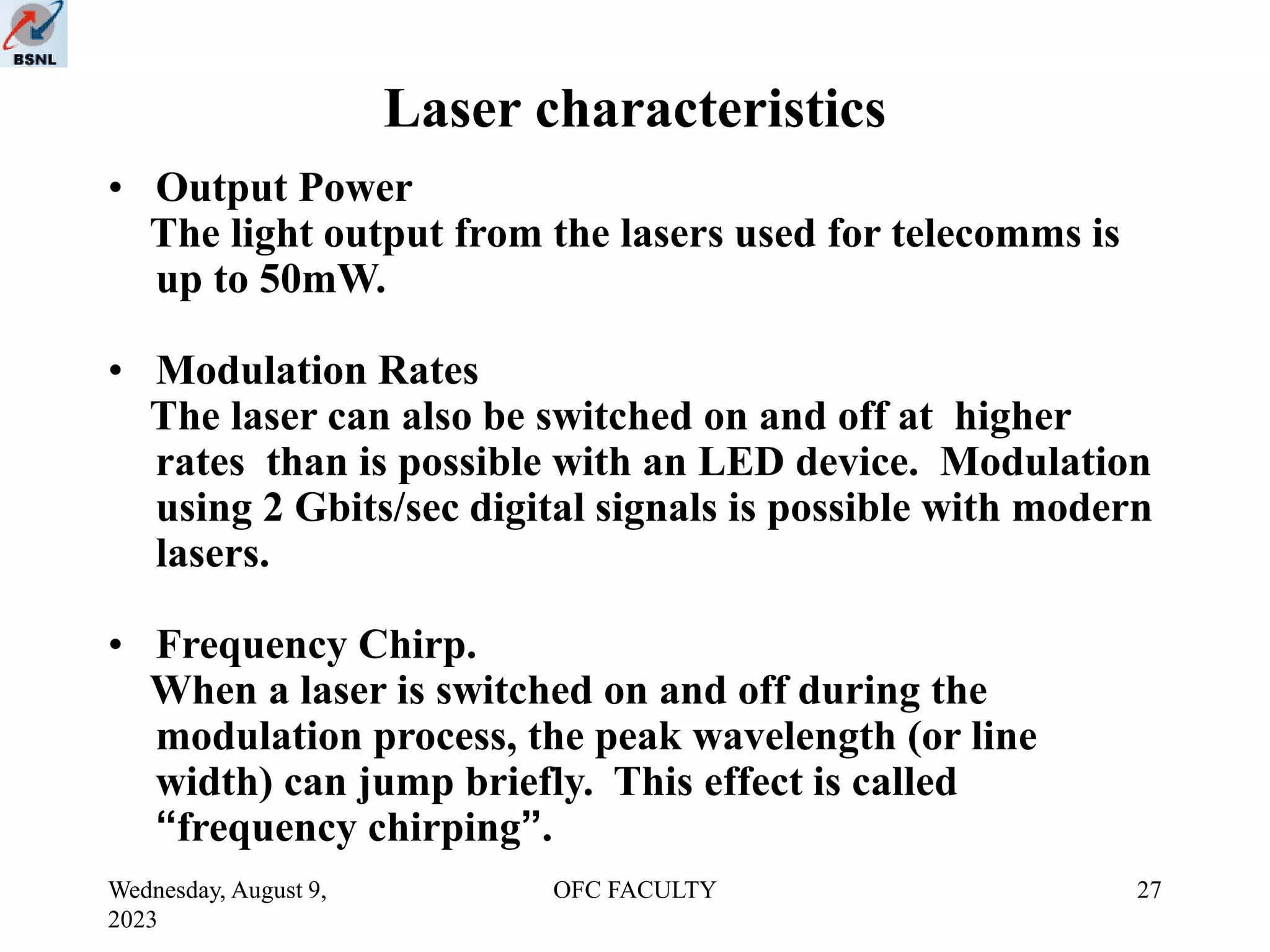
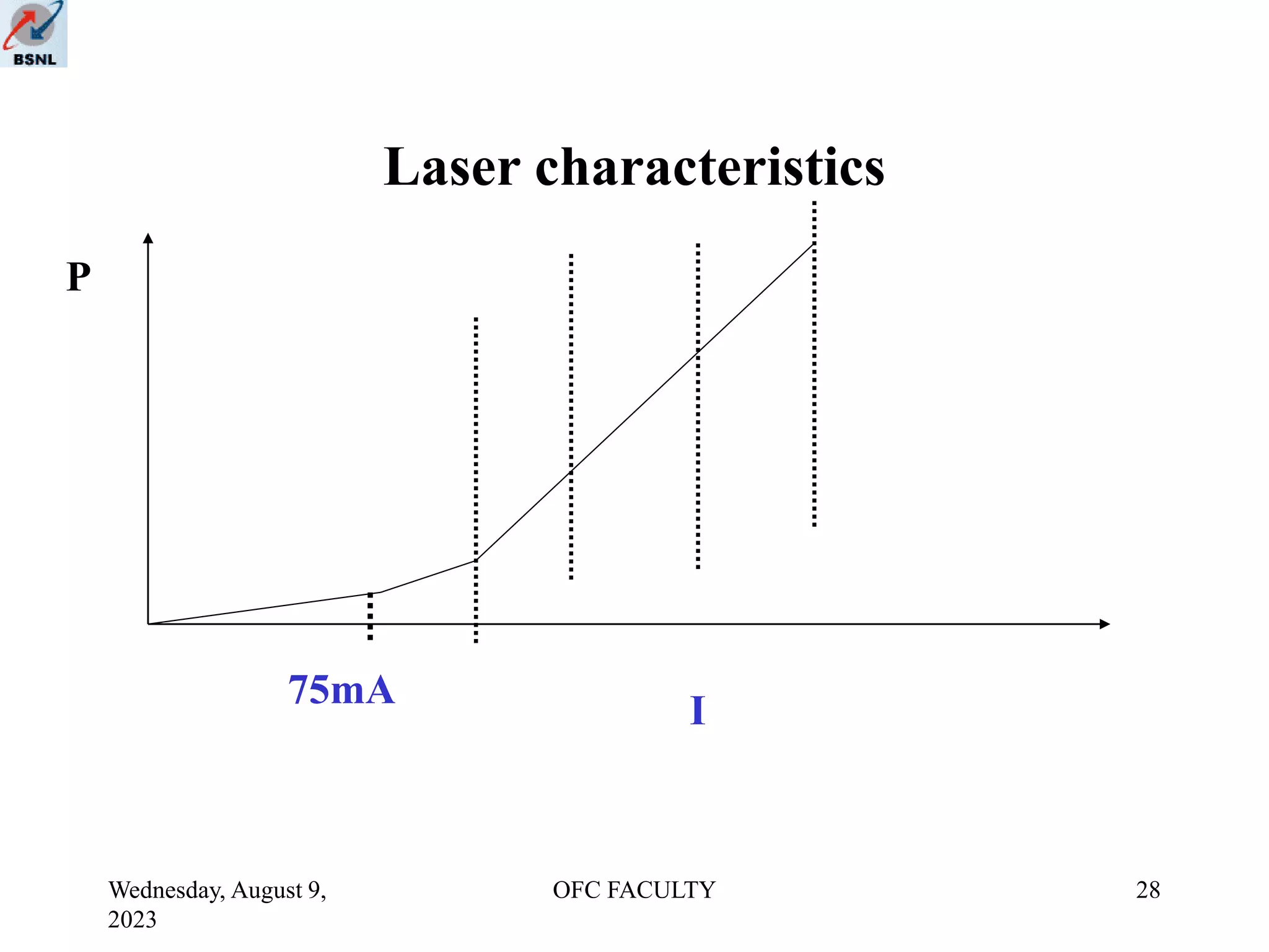
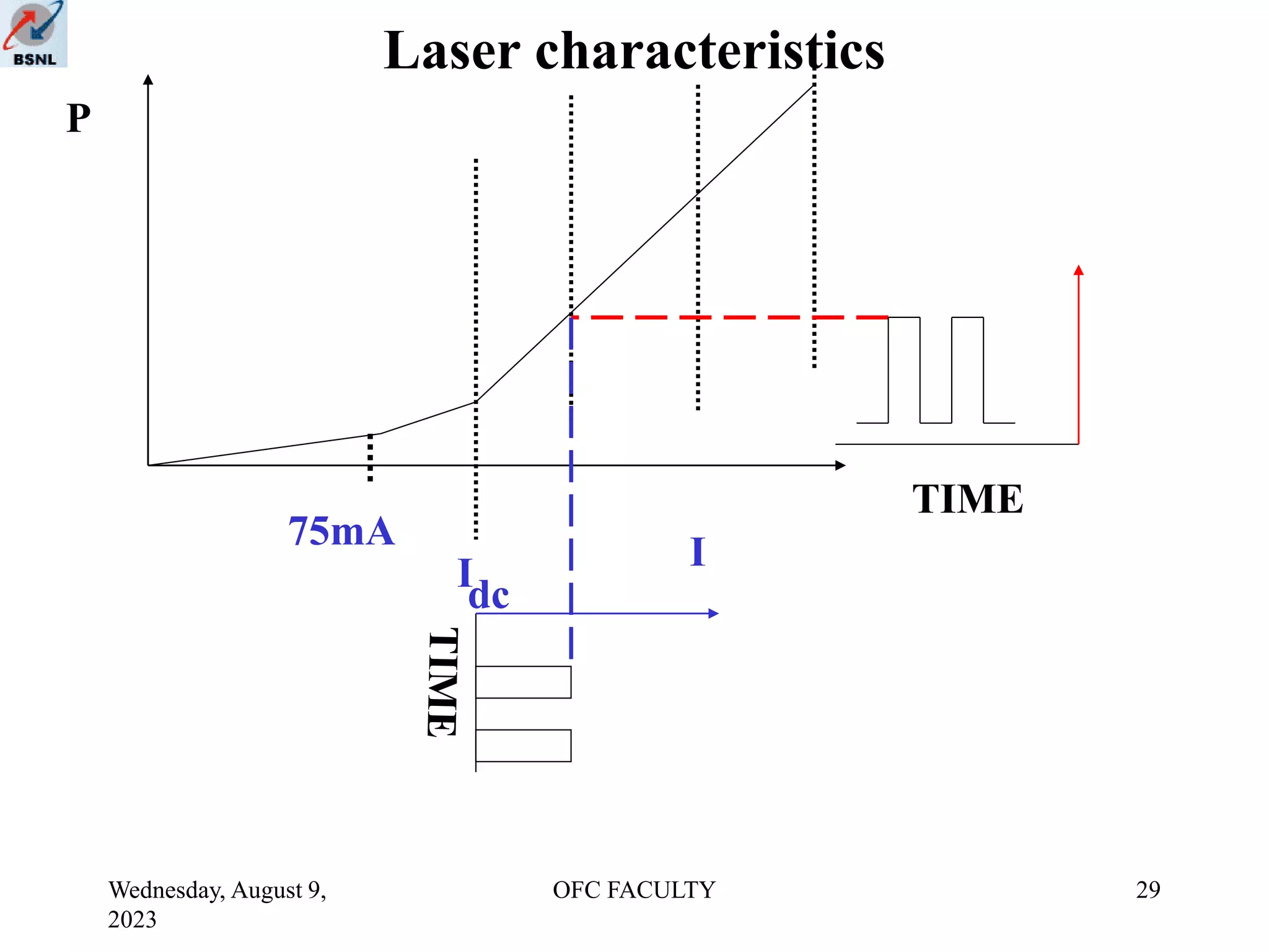
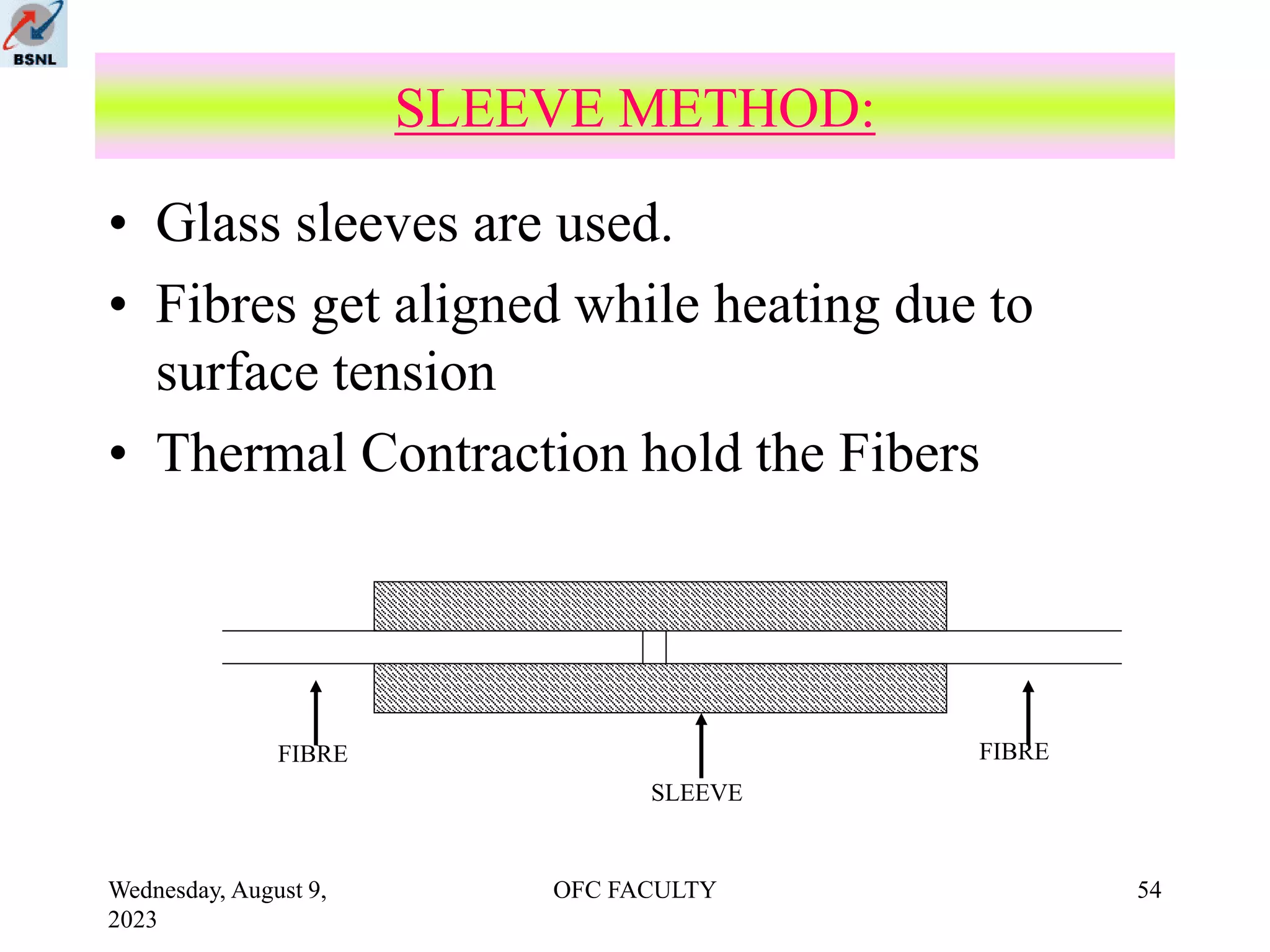
Wednesday, August 9,
2023
OFC FACULTY 1
OPTICAL SOURCES, DETECTOR,
CONNECTORS, COUPLERS ,SPLICES &
INSTRUMENTS
BY
OFC FACULTY
Wednesday, August 9,
2023
OFC FACULTY 2
NEED OF OPTICAL SOURCES
WHY WE NEED TRANSMISSION MEDIA?
X
G
E-
1
X
G
E-
2
OPTICAL
SOURCE
OPTICAL
DETECTOR
Wednesday, August 9,
2023
OFC FACULTY 3
OPTICAL TRANSMITTER
MUX
ELECTRONIC
PROCESSING
OPTICAL
SOURCE
OPTICAL TRANSMITTER
PROCESSING IS DONE ELECTRONICALLY TO
PREPARE THE SIGNAL FOR TRAVELLING SAFE
THROUGH THE FIBER
Wednesday, August 9,
2023
OFC FACULTY 4
FUNCTIONS OF OPTICAL TRANSMITTER
MUX
ELECTRONIC
PROCESSING
OPTICAL
SOURCE
•SEPARATION OF CLOCK & DATA
•LINE CODING - COVERSION INTO
OPTICAL LINE CODING
•SCRAMBLING
•COMBINING ORDERWIRE ,SUPERVISORY
PROTECTION SWITCHING SIGNALS WITH
THE MAIN SIGNAL
Wednesday, August 9,
2023
OFC FACULTY 5
REQUIREMENTS or EXPECTATIONS
FROM OPTICAL SOURCES
•PRIMARY CHARACTERISTIC WAVELENGTH
-LOW ATTENUATION,
-LOW DISPERSION
THREE WINDOWS- 850 , 1300 , 1550nm
Wednesday, August 9,
2023
OFC FACULTY 6
WINDOWS
Wednesday, August 9,
2023
OFC FACULTY 7
REQUIREMENTS or EXPECTATIONS FROM
OPTICAL SOURCES
•RELIABILITY -
- LONG LIFE
- GOOD TEMPERATURE STABILITY
- GOOD REPRODUCIBILITY OF OUTPUT
CHARATERISTICS
AREA OF EMISSION - SMALL (SAME AS THE FIBRE
CORE SIZE)
EMISSION ANGLE - SMALL
LIGHT WAVELENGTH - TO SUIT FIBRE AND
DETECTOR
FAST RESPONSE TO INPUT MODULATION
Wednesday, August 9,
2023
OFC FACULTY 8
REQUIREMENTS or EXPECTATIONS FROM
OPTICAL SOURCES
•OUTPUT POWER -
- SYSTEM DEMANDS MUST BE MET
- > 1 Mw
•POWER EFFICIENCY -
- LOW POWER
- LOW VOLTAGE
- SMALL WASTE HEAT
> 10 % EASY MAINTENANCE
Wednesday, August 9,
2023
OFC FACULTY 9
REQUIREMENTS or EXPECTATIONS FROM
OPTICAL SOURCES
•COST -
•SPECTRAL WIDTH - SINGLE FREQUECY 
MAXIMUM UTILISATION OF THE FIBER BW
PRACTICAL SOURCES FALL SHORT OF
THESE REQUIREMENTS
SPECTRAL WIDTH , STABILITY
FOCUSSING CAPABILITY
HIGH COUPLING EFFICIENCY SHOULD BE POSSIBLE
SIZE & WEIGHT – SMALL,- LIGHT WEIGHT
Wednesday, August 9,
2023
OFC FACULTY 10
LIGHT SOURCES
TWO TYPES OF LIGHT SOURCES
EMPLOYED IN COMMUNICATIONS
- LED
- LD
BOTH USE INTENSITY MODULATION
Wednesday, August 9,
2023
OFC FACULTY 11
LIGHT SOURCES
LED - LIGHT EMITTING DIODE
- SHORTHAULAND MEDIUM HAUL
COMMUNICATION SYSTEMS WHERE
-POWER REQUIREMENTS ARE SMALL
- LOW BIT RATES REQUIRED
LD - LASER DIODE
- USED FOR LONG DISTANCE
- HIGH BIT RATE APPLICATIONS
Wednesday, August 9,
2023
OFC FACULTY 12
Light emitting diodes (LED)
• Light emitting diodes are manufactured from gallium-
aluminium arsenide or arsenide-phosphide materials.
• Using normal semiconductor diffusion growth
techniques, a P- N junction diode is made and
electrons and holes will migrate across this junction
when the diode is forward biased.
• As these carriers recombine, energy is emitted in the
form of light with a wavelength of between 500 and
900nm. This is called “Spontaneous Emission”.
Wednesday, August 9,
2023
OFC FACULTY 13
OPERATING PRINCIPLE
IS A p-n JUNCTION DIODE EMITS LIGHT WHEN FORWARDBIASED
DUE TO RECOMBINATION OF e h IN THE TRANSITION REGION
ENERGY BAND DIAGRAM
E2
E1
E2
E1
Wednesday, August 9,
2023
OFC FACULTY 14
OPERATING PRINCIPLE
EF
e V0
Eg
Conduction band
Conduction band
Valance band
Valance band
n p
V = 0
Wednesday, August 9,
2023
OFC FACULTY 15
OPERATING PRINCIPLE
EF
e V0
Eg
Conduction band
Valance band
Valance band
e (V0-Vi)
n p
Vi
+
Vi
Wednesday, August 9,
2023
OFC FACULTY 16
LED WAVELENGTH OF PHOTON
Eg = h * f
f = c / 
Eg = h * ( c /  )
OR
 = --------- ?
Wednesday, August 9,
2023
OFC FACULTY 17
LED
CHARACTERISTICS
LED CURRENT (in mA)
Wednesday, August 9,
2023
OFC FACULTY 18
LED MODULATION
LED CURRENT (in mA)
OUTPUT
POWER
TIME
Wednesday, August 9,
2023
OFC FACULTY 19
LED STABILITY
LIFE TIME OF LED 10 HOURS
6
TEMPERATURE DEPENDANCE OF LED
Pout reduces 1% per degree C
P
mW
i mA
TO
T3
T2
T1
P = Po [ 1 -  (T-To)]
Wednesday, August 9,
2023
OFC FACULTY 20
LED RADIATION PATTERN
P = k * COS 

-90 O 90
BEAM ANGLE
BEAM INTENSITY
RADIATION PATTERN -
EDGE EMITTERS
CONCENTRATE THEIR
RADIATION BETTER THAN
THE SURFACE EMITTERS
Wednesday, August 9,
2023
OFC FACULTY 21
Disadvantages of LED devices
• The LED produces light which has a BROAD
SPECTRAL RESPONSE, typically 50-100nm. This
means that the light output is not all at the same
wavelength or colour.
• When the LED light is transmitted over long
distances through fibre optic cables some pulse
spreading will occur due to CHROMATIC
DISPERSION in the fibre core.
• The LED is a cheap, reliable light source suitable
for short distance, low speed optical transmission
systems only.
Wednesday, August 9,
2023
OFC FACULTY 22
Laser Diodes
• The LASER (Light Amplification by Stimulated Emission
of Radiation) operates in a manner similar to the LED but
produces a much higher output power.
• The electrons can make jumps from one energy level to
another within an atom. This movement is accompanied
by the emission or absorption of electromagnetic radiation
in the form of “photons”. The frequency of the emitted
radiation is determined by the semiconductor materials
used to make the laser.
Eg = h * ( c /  )
 = --------- ?
Wednesday, August 9,
2023
OFC FACULTY 23
LASER OPERATING PRINCIPLE
ABSORPTION
STIMULATED
EMISSION
SPONTANEOUS
EMSSION
E2
E1
Wednesday, August 9,
2023
OFC FACULTY 24
LASER OPERATING PRINCIPLE
Wednesday, August 9,
2023
OFC FACULTY 25
Producing the light output.
• The PN junction is heavily forward biased creating a
dense population of electrons in the conduction band.
At low current levels the device will generate light by
spontaneous emission just as the LED device.
• Once the threshold current has been exceeded the high
electron density will stimulate light emission and the
photons which are emitted will collide with other atoms
in the semi-conductor material causing more photons to
be emitted. This is called “Stimulated Emission”.
Wednesday, August 9,
2023
OFC FACULTY 26
Laser action
• The active layer is bounded by an optical cavity with
two semi-transparent mirrors ends.
• Photons reaching the outer surface are reflected back
into the material and collides with another electron
causing a second photon to be produced. These two
photons are then reflected and collide with more
electrons and the process is repeated so that a very
large number of photons are created in a short time.
This process is called “Lasing”.
Wednesday, August 9,
2023
OFC FACULTY 27
Laser characteristics
• Output Power
The light output from the lasers used for telecomms is
up to 50mW.
• Modulation Rates
The laser can also be switched on and off at higher
rates than is possible with an LED device. Modulation
using 2 Gbits/sec digital signals is possible with modern
lasers.
• Frequency Chirp.
When a laser is switched on and off during the
modulation process, the peak wavelength (or line
width) can jump briefly. This effect is called
“frequency chirping”.
Wednesday, August 9,
2023
OFC FACULTY 28
Laser characteristics
75mA
I
P
Wednesday, August 9,
2023
OFC FACULTY 29
Laser characteristics
75mA
I
P
I
dc
TIME
Wednesday, August 9,
2023
OFC FACULTY 30
Laser action
Wednesday, August 9,
2023
OFC FACULTY 31
Noise in the laser output.
• When a laser is operating, there are random fluctuations in the
power of the light emitted. This variation can produce noise at the
optical detector. A typical S/N ratio for an injection laser is
around - 80dB.
• When the laser is operating above the cut-off point of its
characteristic, a small change in temperature can cause the output
spectrum to change suddenly as the laser jumps to another mode.
This causes a kink in the characteristic graph.
• Stabilization of mode is achieved by keeping the laser temperature
constant by adequate heat sinks and cooling.
Wednesday, August 9,
2023
OFC FACULTY 32
Heat sinks.
• The threshold current of a laser is dependent on
temperature and, for efficient operation, the optimum
working temperature is 32- 35° C. To maintain this
temperature, very efficient heat sinks are required
and in some cases Peltier heat pumps may be used.
• Many lasers include built-in negative feedback circuits
to control the output power and junction temperature.
If the temperature rises above a safe value, the power
supply automatically shuts down and an alarm
indication is given to the operator.
Wednesday, August 9,
2023
OFC FACULTY 33
Distributed Feedback Lasers.
• Many early laser designs suffered from “mode
instability” and were prone to small frequency changes
as the laser jumped from one mode pattern to another.
(typical 2.0nm width)
• Modern designs, are being introduced with distributed
feedback. These are known as “distributed feedback
lasers”(DFL).
• The optical feedback in these DFL devices is not due to
reflection from the cavity end faces but by a grating
built into the laser which provides feedback along the
whole length of the cavity.
• This type of construction produces a single stable
output frequency and other modes are 20-30db below
the fundamental. (typical 0.2nm width)
Wednesday, August 9,
2023
OFC FACULTY 34
Optical sources compared
Wednesday, August 9,
2023
OFC FACULTY 35
X
G
E-
1
X
G
E-
2
OPTICAL
SOURCE
OPTICAL
DETECTOR
INTRODUCTION
OPTICAL DETECTOR
Wednesday, August 9,
2023
OFC FACULTY 36
INTRODUCTION
•PERFORMS JUST OPPOSITE FUNCTION
TO THAT OF OPTICAL SOURCE
•IS AN OPTO ELECTRONIC
TRANSDUCER
•CONVERTS OPTICAL ENERGY INTO
ELECTRICAL ENERGY
TWO BASIC PHOTODETECTION
MECHANISMS-
EXTERNAL PHOTOELECTRIC EFFECT
AND
INTERNAL PHOTOELECTRIC EFFECT
Wednesday, August 9,
2023
OFC FACULTY 37
INTRODUCTION
EXTERNAL PHOTOELECTRIC EFFECT
ELECTRONS ARE FREED FROM THE SURFACE OF
THE METAL BY THE ENERGY ABSORBED FROM
THE INCIDENT PHOTONS
EXAMPLES ARE
VACCUM PHOTODIODE
PHOTOMULTIPLIER TUBE
Wednesday, August 9,
2023
OFC FACULTY 38
INTRODUCTION
INTERNAL PHOTOELECTRIC EFFECT
FREE CHARGE CARRIERS (ELECTRONS AND
HOLES) ARE GENERATED BY THE ENERGY
ABSORBED FROM THE INCIDENT PHOTONS
EXAMPLES ARE -SEICONDUCTOR JUNCTION
DEVICES--
•PN JUNCTION PHOTODIODE
• PIN PHOTODIODE
•AVALANCHE PHOTODIODE
Wednesday, August 9,
2023
OFC FACULTY 39
SEMICONDUCTOR PHOTODIODES
ABSORBED PHOTONS EXCITE ELECTRONS
FROM VALANCE BAND TO THE CONDUCTION
BAND--INTRINSIC ABSORPTION
THE RESULT IS CREATION OF AN ELECTRON-
HOLE PAIR
THESE CARRIERS UNDER THE INFLUENCE OF
THE BIAS VOLTAGE INDUCE A CURRENT IN THE
EXTERNAL CIRCUIT
Wednesday, August 9,
2023
OFC FACULTY 40
SEMICONDUCTOR PHOTODIODES 2
Wednesday, August 9,
2023
OFC FACULTY 41
PN PHOTODIODE
•NOT WIDELY USED BUT HELPS TO UNDERSTAND
PRINCIPLE OF SEMICONDUCTOR
PHOTODETECTION
•OTHER DEVICES OVERCOME THE LIMITATIONS
OF PN DIODE
Wednesday, August 9,
2023
OFC FACULTY 42
PRINCIPLE
•WHEN RB LITTLE CURRENT FLOWS
•DIPLETION REGION WIDENS
•CARRIERS LEAVE THE JUNCTION
•MOST OF VOLTAGE DROPS ACROSS THE
DEPLETION REGION
•HIGH ELECTRIC FORCES PRESENT
n p
Wednesday, August 9,
2023
OFC FACULTY 43
LIMITATIONS OF PN PD
•MANY OF THE ABSORBED PHOTONS DO NOT
RESULT IN EXTERNAL CURRENT
•BECAUSE THE DEPLATION AREA IS SMALL
PORTION OF DIODE’S TOTAL VOLUME
•HIGH OPTICAL POWER REQUIRED
•THE CURRENT IS DELAYED W.R.T. THE
ABSORPTION OF THE PHOTON --SLOW TAIL
•CAN NOT BE USED FOR HIGH SPEED
APPLICATIONS
Wednesday, August 9,
2023
OFC FACULTY 44
PIN PD
•POSITIVE INTRINSIC NEGATIVE
•LENGTH OF DEPLETION REGION INCRESED BY
•ADDITION OF LIGHTLY DOPED INTRINSIC LAYER
BETWEEN P N LAYERS
i
n p
Wednesday, August 9,
2023
OFC FACULTY 45
PIN PD
•TRDE OFF BETWEEN EFFICIENCY AND SPEED
•PHOTON TO CARRIER CONVERSION EFFICIENCY
REQUIRES A THICK INTRINSIC LAYER TO INCRESE
THE PROBABILITY OF e-h PAIR
•SPEED REQUIRES THINNER LAYER TO REDUCE
THE TRANSIT TIME
Wednesday, August 9,
2023
OFC FACULTY 46
APD
•AVALANCHE PHOTODIODE
•FEW INCIDENT PHOTONS RESULT IN MANY
CARRIERS , LARGER EXTERNAL CURRENT
•VERY STRONG E-FIELD IN DEPLATION REGION
•PRIMARY CARRIERS (BY ABSORBED PHOTONS)
•PRIMARY CARRIERS -- ARE ACCEERATED BY E-
FIELD-- K.E.
•SECONDARY CARRIERS
•PHOTOMLTIPLICATION
Wednesday, August 9,
2023
OFC FACULTY 47
DETECTOR - CHARACTERISTICS
•RESPONSIVITY= P =(OUTPUT CURRENT)/(INPUT
OPTICAL POWER)
P=0.6 A/W PIN
P=75 A/W APD
Popt incident = 50 micro Watts will give I PIN =30 micro A
I APD =3.75 mA
Wednesday, August 9,
2023
OFC FACULTY 48
DETECTOR - CHARACTERISTICS
•QUANTUM EFFICIENCY= (No. of photons causing
generation of primary e-h pair)/(total no. of incident
photons)
DARK CURRENT
THERMALLY GENERATED
PRESENT EVEN WHEN NO OPT-POWER
SMALL R.B. CURRENT
MINIMUM DETECTABLE POWER
LOWEST LEVEL OF INCIDENT OPTICAL-POWER
THE DETECTOR CAN HANDLEDARK CURRENT=
Wednesday, August 9,
2023
OFC FACULTY 49
CONNECTORS, COUPLERS & SPLICES.
• JOINING OF OPTICAL FIBRE IS ESSENTIAL FOR MEETING THE
VARIOUS REQUIREMENTS OF FIBRE COMMUNICATION:
–TO INCREASE THE CABLE LENGTH.
MEANS OF JOINING IN O.F. CABLE :
–TO EXTEND THE OPTICAL SIGNAL TO TESTING INSTRUMENTS.
–TO EXTEND THE OPTICAL SIGNAL FROM FIBER TO THE
EQUIPMENT & VICE-VERSA.
1. CONNECTOR
2. COUPLER
3. SPLICES
Wednesday, August 9,
2023
OFC FACULTY 50
ARRANGING TRANSFER OF OPTICAL ENERGY FROM
ONE FIBRE OPTIC COMPONENT TO ANOTHER IN AN
O.F.SYSTEM.
CONNECTORS, COUPLERS & SPLICES.
A MULTIPORT DEVICES WHICH PERMIT TRANSFER
OF OPTIC POWER FROM ONE PORT TO ALL OTHER
SIMULTANEOUSLY & VICE-VERSA
PERMANENT JOINTS BETWEEN TWO FIBRES.
–BETTER JOINTING : LOWER LOSS
–LONGER LINK IS POSSIBLE WITH SOME OPTICAL POWER.
CONNECTORS:
COUPLERS:
SPLICES:
SIGNIFICANT OF THE ABOVE IN FIBRE OPTIC COMMUNICATION:
Wednesday, August 9,
2023
OFC FACULTY 51
1. Attenuation  0.5 dB
2. Protection of the fibre
3. Simple technique for connection
4. Size (Not too big as compare To the fibre)
5. Cost Effective
CONNECTOR REQUIREMENT
Wednesday, August 9,
2023
OFC FACULTY 52
1. ADAPTER
– PROVIDE ALIGNMENT MECHANISM
– USUALLY METALLIC
– DEVICES MAY BE HOUSED IN ADAPTER PARTS CALLED
RECEPTACLE
2. PLUGS
– PROVIDED WITH SCREWS / LOCKING MECH FOR
REMATING PURPOSE
– FIBRE FIXING MAY BE DONE DIRECTLY OR BY USING
SLEEVES OR FERRULES
TO MEET OUT THE NEEDS ; A HIGH DEGREE OF
ALIGNMENT IS REQD.
CONNECTOR COMPOSITION
Wednesday, August 9,
2023
OFC FACULTY 53
SPLICES :
A PERMANENT CONNECTION BETWEEN TWO
FIBRES.
SPLICING PROCESS INVOLVES:
– CUTTING THE EDGES OF TWO FIBRES.
– TWO FIBRES ENDS MADE TO BUTT POSN AGAINST
EACH OTHER
– FIXING PERMANENTLY & REINFOECED
– MECHANICALLY FIXED PERMANENTALY THROUGH
USE OF EPOXIES OR FUSION
Wednesday, August 9,
2023
OFC FACULTY 54
• Glass sleeves are used.
• Fibres get aligned while heating due to
surface tension
• Thermal Contraction hold the Fibers
SLEEVE METHOD:
FIBRE
SLEEVE
FIBRE
Wednesday, August 9,
2023
OFC FACULTY 55
• Welding of the fibres
• To achieve very low splice losses
• Fusion Through Electric arc.
• Removal of primary coating
• Fibres edge preparation
• Fixing the fibres in micro position
• Align the fibres through microscopic sights fixed on
machine or by monitoring on a video monitor.
• Machine is Microprocessor controlled
• Fusion
• Reinforcement
FUSION METHOD
Wednesday, August 9,
2023
OFC FACULTY 56
Wednesday, August 9,
2023
OFC FACULTY 57
• Calibrated Light Source.
• Optical Power Meter.
• Optical Attenuator.
• Optical Time Domain Reflectometer
(OTDR).
INSTRUMENTS REQUIRED
Wednesday, August 9,
2023
OFC FACULTY 58
• Generates Light signals of known
power and wavelength (LED or
LASER).
• Wavelength variations to match
Fiber's Wavelength.
CALIBRATED LIGHT SOURCE
Wednesday, August 9,
2023
OFC FACULTY 59
• Measures Optical Power over wide range
(Typically 1 nW to 2mW/-60dBm to + 3dBm)
• It is never measured directly, but measured
through Electrical conversion using Photo
Electric conversion. It is known as OPTICAL
SENSOR of known Wavelength.
• The accuracy of the Optical Power meter
depends upon the stability of the Detector’s
power to current conversion which changes
with Ageing.
OPTICAL POWER METER
Wednesday, August 9,
2023
OFC FACULTY 60
• TYPES:-
– Fixed Attenuators.
– Variable Attenuators.
• APPLICATIONS:-
– To Simulate the Regenerator Hop Loss at the FDF.
– To Provide Local Loop Back for Testing.
– To measure the Bit Error Rate by varying the Optical
Signal at the Receiver Input.
(RECEIVER SENSITIVITY)
OPTICAL ATTENUATORS
Wednesday, August 9,
2023
OFC FACULTY 61
REQUIREMENTS OF
ATTENUATORS
• Attenuation Range.
• Lowest Insertion Loss.
• Independent of Wavelength.
• Type of Connectors at the Input and Output.
Wednesday, August 9,
2023
OFC FACULTY 62
Fiber
Light Source
Light Source
100%
Dark
Light Receiver
Fiber
Motion
0%
Dark
(VARIABLE ATTENUATOR)
Wednesday, August 9,
2023
OFC FACULTY 63
• Used for measuring
– Fiber Loss.
– Splice Loss.
– Connector Loss.
– Fiber Length.
– Continuity of Fiber.
– Fault Localization.
OPTICAL TIME DOMAIN REFLECTOMETER
(OTDR)
Wednesday, August 9,
2023
OFC FACULTY 64
• One Port Operation.
• Works on the Principle of Back Scattering
(Raleigh Scattering, see Figure ).
– Scattering is the main cause of Fiber Loss
– Scattering Coefficient=1/4
– An Optical Pulse is launched into one End of
Fiber and Back Scattered Signals are detected.
– These Signals are approximately 50 dB below
the Transmitted level.
• Measuring conditions and Results are displayed.
OPERAING PRINCIPLES
Wednesday, August 9,
2023
OFC FACULTY 65
OTDR INSTRUMENT PRINCIPLE
Fiber
APD
Signal
Oscilloscope Amplifier
Trigger
Pulse
Generator
Laser
Wednesday, August 9,
2023
OFC FACULTY 66
Reflections show OTDR
Pulse Width and Resolution
Connectors show both
Loss and Reflections
Splices are usually
not Reflective.
Splices Loss
Slope of trace shows Fiber
Attenuation Coefficient
OTDR Trace Information
Wednesday, August 9,
2023
OFC FACULTY 67
Splice Loss Measurement Principles
The trace waveform at the Splice Point should be displayed as the dotted line in
the figure below, but is actually displayed as the solid line. The waveform input
to the OTDR shows a sharp falling edge at the splice point, so the circuit cannot
respond correctly. The interval L gets longer as the pulse width becomes longer.
Splice Point
L
Therefore, the Splice Loss can not be measured correctly in the Loss Mode.
Wednesday, August 9,
2023
OFC FACULTY 68
•In the Splice Loss mode, two markers are set on each side of the Splice
Point and the lines L1 and L2 are drawn as shown below. The part of the straight
line immediately after the splice point is the forward projection of the straight
line, L2
•The Splice Loss is found by dropping a vertical line from the Splice Point to this
projection of L2, and measuring the level difference between the Splice Point and
the intersection.
x1
x2
x3
x4
L2
Splice Loss
Splice Point
L1

OPTICAL-SOURCE

  • 1.
    Wednesday, August 9, 2023 OFCFACULTY 1 OPTICAL SOURCES, DETECTOR, CONNECTORS, COUPLERS ,SPLICES & INSTRUMENTS BY OFC FACULTY
  • 2.
    Wednesday, August 9, 2023 OFCFACULTY 2 NEED OF OPTICAL SOURCES WHY WE NEED TRANSMISSION MEDIA? X G E- 1 X G E- 2 OPTICAL SOURCE OPTICAL DETECTOR
  • 3.
    Wednesday, August 9, 2023 OFCFACULTY 3 OPTICAL TRANSMITTER MUX ELECTRONIC PROCESSING OPTICAL SOURCE OPTICAL TRANSMITTER PROCESSING IS DONE ELECTRONICALLY TO PREPARE THE SIGNAL FOR TRAVELLING SAFE THROUGH THE FIBER
  • 4.
    Wednesday, August 9, 2023 OFCFACULTY 4 FUNCTIONS OF OPTICAL TRANSMITTER MUX ELECTRONIC PROCESSING OPTICAL SOURCE •SEPARATION OF CLOCK & DATA •LINE CODING - COVERSION INTO OPTICAL LINE CODING •SCRAMBLING •COMBINING ORDERWIRE ,SUPERVISORY PROTECTION SWITCHING SIGNALS WITH THE MAIN SIGNAL
  • 5.
    Wednesday, August 9, 2023 OFCFACULTY 5 REQUIREMENTS or EXPECTATIONS FROM OPTICAL SOURCES •PRIMARY CHARACTERISTIC WAVELENGTH -LOW ATTENUATION, -LOW DISPERSION THREE WINDOWS- 850 , 1300 , 1550nm
  • 6.
  • 7.
    Wednesday, August 9, 2023 OFCFACULTY 7 REQUIREMENTS or EXPECTATIONS FROM OPTICAL SOURCES •RELIABILITY - - LONG LIFE - GOOD TEMPERATURE STABILITY - GOOD REPRODUCIBILITY OF OUTPUT CHARATERISTICS AREA OF EMISSION - SMALL (SAME AS THE FIBRE CORE SIZE) EMISSION ANGLE - SMALL LIGHT WAVELENGTH - TO SUIT FIBRE AND DETECTOR FAST RESPONSE TO INPUT MODULATION
  • 8.
    Wednesday, August 9, 2023 OFCFACULTY 8 REQUIREMENTS or EXPECTATIONS FROM OPTICAL SOURCES •OUTPUT POWER - - SYSTEM DEMANDS MUST BE MET - > 1 Mw •POWER EFFICIENCY - - LOW POWER - LOW VOLTAGE - SMALL WASTE HEAT > 10 % EASY MAINTENANCE
  • 9.
    Wednesday, August 9, 2023 OFCFACULTY 9 REQUIREMENTS or EXPECTATIONS FROM OPTICAL SOURCES •COST - •SPECTRAL WIDTH - SINGLE FREQUECY MAXIMUM UTILISATION OF THE FIBER BW PRACTICAL SOURCES FALL SHORT OF THESE REQUIREMENTS SPECTRAL WIDTH , STABILITY FOCUSSING CAPABILITY HIGH COUPLING EFFICIENCY SHOULD BE POSSIBLE SIZE & WEIGHT – SMALL,- LIGHT WEIGHT
  • 10.
    Wednesday, August 9, 2023 OFCFACULTY 10 LIGHT SOURCES TWO TYPES OF LIGHT SOURCES EMPLOYED IN COMMUNICATIONS - LED - LD BOTH USE INTENSITY MODULATION
  • 11.
    Wednesday, August 9, 2023 OFCFACULTY 11 LIGHT SOURCES LED - LIGHT EMITTING DIODE - SHORTHAULAND MEDIUM HAUL COMMUNICATION SYSTEMS WHERE -POWER REQUIREMENTS ARE SMALL - LOW BIT RATES REQUIRED LD - LASER DIODE - USED FOR LONG DISTANCE - HIGH BIT RATE APPLICATIONS
  • 12.
    Wednesday, August 9, 2023 OFCFACULTY 12 Light emitting diodes (LED) • Light emitting diodes are manufactured from gallium- aluminium arsenide or arsenide-phosphide materials. • Using normal semiconductor diffusion growth techniques, a P- N junction diode is made and electrons and holes will migrate across this junction when the diode is forward biased. • As these carriers recombine, energy is emitted in the form of light with a wavelength of between 500 and 900nm. This is called “Spontaneous Emission”.
  • 13.
    Wednesday, August 9, 2023 OFCFACULTY 13 OPERATING PRINCIPLE IS A p-n JUNCTION DIODE EMITS LIGHT WHEN FORWARDBIASED DUE TO RECOMBINATION OF e h IN THE TRANSITION REGION ENERGY BAND DIAGRAM E2 E1 E2 E1
  • 14.
    Wednesday, August 9, 2023 OFCFACULTY 14 OPERATING PRINCIPLE EF e V0 Eg Conduction band Conduction band Valance band Valance band n p V = 0
  • 15.
    Wednesday, August 9, 2023 OFCFACULTY 15 OPERATING PRINCIPLE EF e V0 Eg Conduction band Valance band Valance band e (V0-Vi) n p Vi + Vi
  • 16.
    Wednesday, August 9, 2023 OFCFACULTY 16 LED WAVELENGTH OF PHOTON Eg = h * f f = c /  Eg = h * ( c /  ) OR  = --------- ?
  • 17.
    Wednesday, August 9, 2023 OFCFACULTY 17 LED CHARACTERISTICS LED CURRENT (in mA)
  • 18.
    Wednesday, August 9, 2023 OFCFACULTY 18 LED MODULATION LED CURRENT (in mA) OUTPUT POWER TIME
  • 19.
    Wednesday, August 9, 2023 OFCFACULTY 19 LED STABILITY LIFE TIME OF LED 10 HOURS 6 TEMPERATURE DEPENDANCE OF LED Pout reduces 1% per degree C P mW i mA TO T3 T2 T1 P = Po [ 1 -  (T-To)]
  • 20.
    Wednesday, August 9, 2023 OFCFACULTY 20 LED RADIATION PATTERN P = k * COS   -90 O 90 BEAM ANGLE BEAM INTENSITY RADIATION PATTERN - EDGE EMITTERS CONCENTRATE THEIR RADIATION BETTER THAN THE SURFACE EMITTERS
  • 21.
    Wednesday, August 9, 2023 OFCFACULTY 21 Disadvantages of LED devices • The LED produces light which has a BROAD SPECTRAL RESPONSE, typically 50-100nm. This means that the light output is not all at the same wavelength or colour. • When the LED light is transmitted over long distances through fibre optic cables some pulse spreading will occur due to CHROMATIC DISPERSION in the fibre core. • The LED is a cheap, reliable light source suitable for short distance, low speed optical transmission systems only.
  • 22.
    Wednesday, August 9, 2023 OFCFACULTY 22 Laser Diodes • The LASER (Light Amplification by Stimulated Emission of Radiation) operates in a manner similar to the LED but produces a much higher output power. • The electrons can make jumps from one energy level to another within an atom. This movement is accompanied by the emission or absorption of electromagnetic radiation in the form of “photons”. The frequency of the emitted radiation is determined by the semiconductor materials used to make the laser. Eg = h * ( c /  )  = --------- ?
  • 23.
    Wednesday, August 9, 2023 OFCFACULTY 23 LASER OPERATING PRINCIPLE ABSORPTION STIMULATED EMISSION SPONTANEOUS EMSSION E2 E1
  • 24.
    Wednesday, August 9, 2023 OFCFACULTY 24 LASER OPERATING PRINCIPLE
  • 25.
    Wednesday, August 9, 2023 OFCFACULTY 25 Producing the light output. • The PN junction is heavily forward biased creating a dense population of electrons in the conduction band. At low current levels the device will generate light by spontaneous emission just as the LED device. • Once the threshold current has been exceeded the high electron density will stimulate light emission and the photons which are emitted will collide with other atoms in the semi-conductor material causing more photons to be emitted. This is called “Stimulated Emission”.
  • 26.
    Wednesday, August 9, 2023 OFCFACULTY 26 Laser action • The active layer is bounded by an optical cavity with two semi-transparent mirrors ends. • Photons reaching the outer surface are reflected back into the material and collides with another electron causing a second photon to be produced. These two photons are then reflected and collide with more electrons and the process is repeated so that a very large number of photons are created in a short time. This process is called “Lasing”.
  • 27.
    Wednesday, August 9, 2023 OFCFACULTY 27 Laser characteristics • Output Power The light output from the lasers used for telecomms is up to 50mW. • Modulation Rates The laser can also be switched on and off at higher rates than is possible with an LED device. Modulation using 2 Gbits/sec digital signals is possible with modern lasers. • Frequency Chirp. When a laser is switched on and off during the modulation process, the peak wavelength (or line width) can jump briefly. This effect is called “frequency chirping”.
  • 28.
    Wednesday, August 9, 2023 OFCFACULTY 28 Laser characteristics 75mA I P
  • 29.
    Wednesday, August 9, 2023 OFCFACULTY 29 Laser characteristics 75mA I P I dc TIME
  • 30.
    Wednesday, August 9, 2023 OFCFACULTY 30 Laser action
  • 31.
    Wednesday, August 9, 2023 OFCFACULTY 31 Noise in the laser output. • When a laser is operating, there are random fluctuations in the power of the light emitted. This variation can produce noise at the optical detector. A typical S/N ratio for an injection laser is around - 80dB. • When the laser is operating above the cut-off point of its characteristic, a small change in temperature can cause the output spectrum to change suddenly as the laser jumps to another mode. This causes a kink in the characteristic graph. • Stabilization of mode is achieved by keeping the laser temperature constant by adequate heat sinks and cooling.
  • 32.
    Wednesday, August 9, 2023 OFCFACULTY 32 Heat sinks. • The threshold current of a laser is dependent on temperature and, for efficient operation, the optimum working temperature is 32- 35° C. To maintain this temperature, very efficient heat sinks are required and in some cases Peltier heat pumps may be used. • Many lasers include built-in negative feedback circuits to control the output power and junction temperature. If the temperature rises above a safe value, the power supply automatically shuts down and an alarm indication is given to the operator.
  • 33.
    Wednesday, August 9, 2023 OFCFACULTY 33 Distributed Feedback Lasers. • Many early laser designs suffered from “mode instability” and were prone to small frequency changes as the laser jumped from one mode pattern to another. (typical 2.0nm width) • Modern designs, are being introduced with distributed feedback. These are known as “distributed feedback lasers”(DFL). • The optical feedback in these DFL devices is not due to reflection from the cavity end faces but by a grating built into the laser which provides feedback along the whole length of the cavity. • This type of construction produces a single stable output frequency and other modes are 20-30db below the fundamental. (typical 0.2nm width)
  • 34.
    Wednesday, August 9, 2023 OFCFACULTY 34 Optical sources compared
  • 35.
    Wednesday, August 9, 2023 OFCFACULTY 35 X G E- 1 X G E- 2 OPTICAL SOURCE OPTICAL DETECTOR INTRODUCTION OPTICAL DETECTOR
  • 36.
    Wednesday, August 9, 2023 OFCFACULTY 36 INTRODUCTION •PERFORMS JUST OPPOSITE FUNCTION TO THAT OF OPTICAL SOURCE •IS AN OPTO ELECTRONIC TRANSDUCER •CONVERTS OPTICAL ENERGY INTO ELECTRICAL ENERGY TWO BASIC PHOTODETECTION MECHANISMS- EXTERNAL PHOTOELECTRIC EFFECT AND INTERNAL PHOTOELECTRIC EFFECT
  • 37.
    Wednesday, August 9, 2023 OFCFACULTY 37 INTRODUCTION EXTERNAL PHOTOELECTRIC EFFECT ELECTRONS ARE FREED FROM THE SURFACE OF THE METAL BY THE ENERGY ABSORBED FROM THE INCIDENT PHOTONS EXAMPLES ARE VACCUM PHOTODIODE PHOTOMULTIPLIER TUBE
  • 38.
    Wednesday, August 9, 2023 OFCFACULTY 38 INTRODUCTION INTERNAL PHOTOELECTRIC EFFECT FREE CHARGE CARRIERS (ELECTRONS AND HOLES) ARE GENERATED BY THE ENERGY ABSORBED FROM THE INCIDENT PHOTONS EXAMPLES ARE -SEICONDUCTOR JUNCTION DEVICES-- •PN JUNCTION PHOTODIODE • PIN PHOTODIODE •AVALANCHE PHOTODIODE
  • 39.
    Wednesday, August 9, 2023 OFCFACULTY 39 SEMICONDUCTOR PHOTODIODES ABSORBED PHOTONS EXCITE ELECTRONS FROM VALANCE BAND TO THE CONDUCTION BAND--INTRINSIC ABSORPTION THE RESULT IS CREATION OF AN ELECTRON- HOLE PAIR THESE CARRIERS UNDER THE INFLUENCE OF THE BIAS VOLTAGE INDUCE A CURRENT IN THE EXTERNAL CIRCUIT
  • 40.
    Wednesday, August 9, 2023 OFCFACULTY 40 SEMICONDUCTOR PHOTODIODES 2
  • 41.
    Wednesday, August 9, 2023 OFCFACULTY 41 PN PHOTODIODE •NOT WIDELY USED BUT HELPS TO UNDERSTAND PRINCIPLE OF SEMICONDUCTOR PHOTODETECTION •OTHER DEVICES OVERCOME THE LIMITATIONS OF PN DIODE
  • 42.
    Wednesday, August 9, 2023 OFCFACULTY 42 PRINCIPLE •WHEN RB LITTLE CURRENT FLOWS •DIPLETION REGION WIDENS •CARRIERS LEAVE THE JUNCTION •MOST OF VOLTAGE DROPS ACROSS THE DEPLETION REGION •HIGH ELECTRIC FORCES PRESENT n p
  • 43.
    Wednesday, August 9, 2023 OFCFACULTY 43 LIMITATIONS OF PN PD •MANY OF THE ABSORBED PHOTONS DO NOT RESULT IN EXTERNAL CURRENT •BECAUSE THE DEPLATION AREA IS SMALL PORTION OF DIODE’S TOTAL VOLUME •HIGH OPTICAL POWER REQUIRED •THE CURRENT IS DELAYED W.R.T. THE ABSORPTION OF THE PHOTON --SLOW TAIL •CAN NOT BE USED FOR HIGH SPEED APPLICATIONS
  • 44.
    Wednesday, August 9, 2023 OFCFACULTY 44 PIN PD •POSITIVE INTRINSIC NEGATIVE •LENGTH OF DEPLETION REGION INCRESED BY •ADDITION OF LIGHTLY DOPED INTRINSIC LAYER BETWEEN P N LAYERS i n p
  • 45.
    Wednesday, August 9, 2023 OFCFACULTY 45 PIN PD •TRDE OFF BETWEEN EFFICIENCY AND SPEED •PHOTON TO CARRIER CONVERSION EFFICIENCY REQUIRES A THICK INTRINSIC LAYER TO INCRESE THE PROBABILITY OF e-h PAIR •SPEED REQUIRES THINNER LAYER TO REDUCE THE TRANSIT TIME
  • 46.
    Wednesday, August 9, 2023 OFCFACULTY 46 APD •AVALANCHE PHOTODIODE •FEW INCIDENT PHOTONS RESULT IN MANY CARRIERS , LARGER EXTERNAL CURRENT •VERY STRONG E-FIELD IN DEPLATION REGION •PRIMARY CARRIERS (BY ABSORBED PHOTONS) •PRIMARY CARRIERS -- ARE ACCEERATED BY E- FIELD-- K.E. •SECONDARY CARRIERS •PHOTOMLTIPLICATION
  • 47.
    Wednesday, August 9, 2023 OFCFACULTY 47 DETECTOR - CHARACTERISTICS •RESPONSIVITY= P =(OUTPUT CURRENT)/(INPUT OPTICAL POWER) P=0.6 A/W PIN P=75 A/W APD Popt incident = 50 micro Watts will give I PIN =30 micro A I APD =3.75 mA
  • 48.
    Wednesday, August 9, 2023 OFCFACULTY 48 DETECTOR - CHARACTERISTICS •QUANTUM EFFICIENCY= (No. of photons causing generation of primary e-h pair)/(total no. of incident photons) DARK CURRENT THERMALLY GENERATED PRESENT EVEN WHEN NO OPT-POWER SMALL R.B. CURRENT MINIMUM DETECTABLE POWER LOWEST LEVEL OF INCIDENT OPTICAL-POWER THE DETECTOR CAN HANDLEDARK CURRENT=
  • 49.
    Wednesday, August 9, 2023 OFCFACULTY 49 CONNECTORS, COUPLERS & SPLICES. • JOINING OF OPTICAL FIBRE IS ESSENTIAL FOR MEETING THE VARIOUS REQUIREMENTS OF FIBRE COMMUNICATION: –TO INCREASE THE CABLE LENGTH. MEANS OF JOINING IN O.F. CABLE : –TO EXTEND THE OPTICAL SIGNAL TO TESTING INSTRUMENTS. –TO EXTEND THE OPTICAL SIGNAL FROM FIBER TO THE EQUIPMENT & VICE-VERSA. 1. CONNECTOR 2. COUPLER 3. SPLICES
  • 50.
    Wednesday, August 9, 2023 OFCFACULTY 50 ARRANGING TRANSFER OF OPTICAL ENERGY FROM ONE FIBRE OPTIC COMPONENT TO ANOTHER IN AN O.F.SYSTEM. CONNECTORS, COUPLERS & SPLICES. A MULTIPORT DEVICES WHICH PERMIT TRANSFER OF OPTIC POWER FROM ONE PORT TO ALL OTHER SIMULTANEOUSLY & VICE-VERSA PERMANENT JOINTS BETWEEN TWO FIBRES. –BETTER JOINTING : LOWER LOSS –LONGER LINK IS POSSIBLE WITH SOME OPTICAL POWER. CONNECTORS: COUPLERS: SPLICES: SIGNIFICANT OF THE ABOVE IN FIBRE OPTIC COMMUNICATION:
  • 51.
    Wednesday, August 9, 2023 OFCFACULTY 51 1. Attenuation  0.5 dB 2. Protection of the fibre 3. Simple technique for connection 4. Size (Not too big as compare To the fibre) 5. Cost Effective CONNECTOR REQUIREMENT
  • 52.
    Wednesday, August 9, 2023 OFCFACULTY 52 1. ADAPTER – PROVIDE ALIGNMENT MECHANISM – USUALLY METALLIC – DEVICES MAY BE HOUSED IN ADAPTER PARTS CALLED RECEPTACLE 2. PLUGS – PROVIDED WITH SCREWS / LOCKING MECH FOR REMATING PURPOSE – FIBRE FIXING MAY BE DONE DIRECTLY OR BY USING SLEEVES OR FERRULES TO MEET OUT THE NEEDS ; A HIGH DEGREE OF ALIGNMENT IS REQD. CONNECTOR COMPOSITION
  • 53.
    Wednesday, August 9, 2023 OFCFACULTY 53 SPLICES : A PERMANENT CONNECTION BETWEEN TWO FIBRES. SPLICING PROCESS INVOLVES: – CUTTING THE EDGES OF TWO FIBRES. – TWO FIBRES ENDS MADE TO BUTT POSN AGAINST EACH OTHER – FIXING PERMANENTLY & REINFOECED – MECHANICALLY FIXED PERMANENTALY THROUGH USE OF EPOXIES OR FUSION
  • 54.
    Wednesday, August 9, 2023 OFCFACULTY 54 • Glass sleeves are used. • Fibres get aligned while heating due to surface tension • Thermal Contraction hold the Fibers SLEEVE METHOD: FIBRE SLEEVE FIBRE
  • 55.
    Wednesday, August 9, 2023 OFCFACULTY 55 • Welding of the fibres • To achieve very low splice losses • Fusion Through Electric arc. • Removal of primary coating • Fibres edge preparation • Fixing the fibres in micro position • Align the fibres through microscopic sights fixed on machine or by monitoring on a video monitor. • Machine is Microprocessor controlled • Fusion • Reinforcement FUSION METHOD
  • 56.
  • 57.
    Wednesday, August 9, 2023 OFCFACULTY 57 • Calibrated Light Source. • Optical Power Meter. • Optical Attenuator. • Optical Time Domain Reflectometer (OTDR). INSTRUMENTS REQUIRED
  • 58.
    Wednesday, August 9, 2023 OFCFACULTY 58 • Generates Light signals of known power and wavelength (LED or LASER). • Wavelength variations to match Fiber's Wavelength. CALIBRATED LIGHT SOURCE
  • 59.
    Wednesday, August 9, 2023 OFCFACULTY 59 • Measures Optical Power over wide range (Typically 1 nW to 2mW/-60dBm to + 3dBm) • It is never measured directly, but measured through Electrical conversion using Photo Electric conversion. It is known as OPTICAL SENSOR of known Wavelength. • The accuracy of the Optical Power meter depends upon the stability of the Detector’s power to current conversion which changes with Ageing. OPTICAL POWER METER
  • 60.
    Wednesday, August 9, 2023 OFCFACULTY 60 • TYPES:- – Fixed Attenuators. – Variable Attenuators. • APPLICATIONS:- – To Simulate the Regenerator Hop Loss at the FDF. – To Provide Local Loop Back for Testing. – To measure the Bit Error Rate by varying the Optical Signal at the Receiver Input. (RECEIVER SENSITIVITY) OPTICAL ATTENUATORS
  • 61.
    Wednesday, August 9, 2023 OFCFACULTY 61 REQUIREMENTS OF ATTENUATORS • Attenuation Range. • Lowest Insertion Loss. • Independent of Wavelength. • Type of Connectors at the Input and Output.
  • 62.
    Wednesday, August 9, 2023 OFCFACULTY 62 Fiber Light Source Light Source 100% Dark Light Receiver Fiber Motion 0% Dark (VARIABLE ATTENUATOR)
  • 63.
    Wednesday, August 9, 2023 OFCFACULTY 63 • Used for measuring – Fiber Loss. – Splice Loss. – Connector Loss. – Fiber Length. – Continuity of Fiber. – Fault Localization. OPTICAL TIME DOMAIN REFLECTOMETER (OTDR)
  • 64.
    Wednesday, August 9, 2023 OFCFACULTY 64 • One Port Operation. • Works on the Principle of Back Scattering (Raleigh Scattering, see Figure ). – Scattering is the main cause of Fiber Loss – Scattering Coefficient=1/4 – An Optical Pulse is launched into one End of Fiber and Back Scattered Signals are detected. – These Signals are approximately 50 dB below the Transmitted level. • Measuring conditions and Results are displayed. OPERAING PRINCIPLES
  • 65.
    Wednesday, August 9, 2023 OFCFACULTY 65 OTDR INSTRUMENT PRINCIPLE Fiber APD Signal Oscilloscope Amplifier Trigger Pulse Generator Laser
  • 66.
    Wednesday, August 9, 2023 OFCFACULTY 66 Reflections show OTDR Pulse Width and Resolution Connectors show both Loss and Reflections Splices are usually not Reflective. Splices Loss Slope of trace shows Fiber Attenuation Coefficient OTDR Trace Information
  • 67.
    Wednesday, August 9, 2023 OFCFACULTY 67 Splice Loss Measurement Principles The trace waveform at the Splice Point should be displayed as the dotted line in the figure below, but is actually displayed as the solid line. The waveform input to the OTDR shows a sharp falling edge at the splice point, so the circuit cannot respond correctly. The interval L gets longer as the pulse width becomes longer. Splice Point L Therefore, the Splice Loss can not be measured correctly in the Loss Mode.
  • 68.
    Wednesday, August 9, 2023 OFCFACULTY 68 •In the Splice Loss mode, two markers are set on each side of the Splice Point and the lines L1 and L2 are drawn as shown below. The part of the straight line immediately after the splice point is the forward projection of the straight line, L2 •The Splice Loss is found by dropping a vertical line from the Splice Point to this projection of L2, and measuring the level difference between the Splice Point and the intersection. x1 x2 x3 x4 L2 Splice Loss Splice Point L1