Download to read offline


![International Research Journal of Engineering and Technology (IRJET) e-ISSN: 2395 -0056
Volume: 04 Issue: 06 | June -2017 www.irjet.net p-ISSN: 2395-0072
© 2017, IRJET | Impact Factor value: 5.181 | ISO 9001:2008 Certified Journal | Page 1699
Fig.4.4. Full Adder test bench program written in Verilog
HDL using Xilinx 14.7
Fig.4.5. Timing diagram obtained after writing the test bench
showing the logical verification of the full adder
6. FUTURE SCOPE
Engineers and Engineering students can easily be able
design their own circuits and implement.Itwill becomevery
easier to showcase their engineering work as per the global
sections of electronics and communication engineering
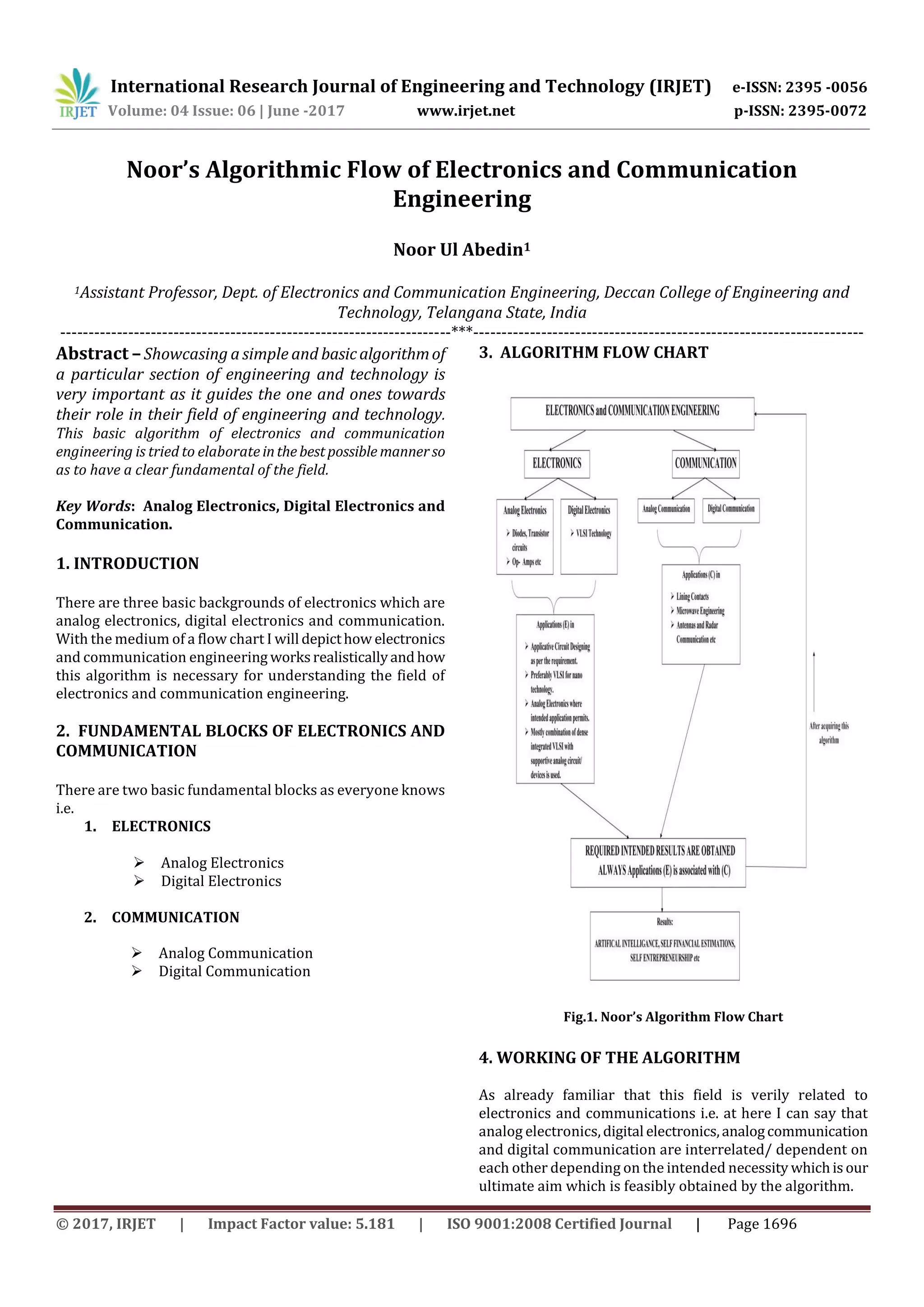
7. CONCLUSION
The importance and use of analog, digital and their
combined effort is understood.
REFERENCES
[1]. Data and Computer Communication Networks by
William Stallings
[2]. Verilog HDL by Samir Palnitkar
[3]. A Verilog HDL Primer by J. Bhasker
[4]. Introduction to VLSI Circuits andSystemsbyJohnP.
Uyemura
[5]. VLSI Design by P Sahu
[6]. VLSI Design by M. Michael Vai
[7]. Digital Systems by Tocci & Widmer
[8]. Digital Design by Morris Mano
[9]. Digital Hardware Design by John B. Peatman
[10]. Antennas by John D Kraus, Ronald J Marhefka and
Ahmed S Khan
[11]. Antenna and Wave Propagation by K. D. Prasad
[12]. Antenna Theory by Constantine Balanis
[13]. Elements of Electromagnetics by Mattew N. O.
Sadiku
[14]. Fundamental of Electronic Circuits by Charles K.
Alexander and Mattew N. O. Sadiku
[15]. Electronic Devices and Circuits by Jacob Millman,
Christos C. Halkias and Satyarbrata Jit
[16]. Electronic Devices and Circuits by S. Salivahanan, N
Kumar and A Vallavaraj
[17]. Integrated Electronics by Jacob Millman, ChristosC.
Halkias and Chetan Parikh
[18]. Circuits and Networks by A Sudhakar and
Shyammohan S Palli
[19]. Engineering Circuit Analysis by W H Hayt,
J E Kemmerly and S M Durbin
[20]. Electronic Devices and Circuits by J B Gupta
BIOGRAPHY
Mr. Noor Ul Abedin is working as
an Assistant Professor in Dept. of
Electronics and Communication,
Deccan College of Engineering and
Technology. He’s field of interest
are Analog and Digital Electronics.
He has lectured and thought
variousengineeringsubjectswhich
include Anlaog Electronic Devices
& Circuits, VLSI Design, Networks
& Circuits, Antennas & Wave
Propagation, Electronic
Instrumentation, Automation in
Process Control, Power
Electronics, Digital Electronics &
Logic Design and LinearIntegrated
Circuits.](https://image.slidesharecdn.com/irjet-v4i6554-180222092707/85/Noor-s-Algorithmic-Flow-of-Electronics-and-Communication-Engineering-4-320.jpg)

This document outlines an algorithmic flowchart for electronics and communication engineering. It begins with an introduction to analog electronics, digital electronics, and communication. The fundamental blocks are then described as analog electronics, digital electronics, and analog and digital communication. A flow chart is presented showing the interrelationships between these areas. The document then discusses how analog and digital electronics and communication relate and provide examples of applications in both fields. It concludes by emphasizing the importance of understanding both analog and digital aspects and their combined use in engineering applications.