Transducers
6
• An electricaltransducer may be defined as a device that
monitors a quantity and converts it into an electrical signal
for measurement or for controlling an industrial operation.
7.
Classification of Transducers
7
•Based on quantity monitored:
• Force, pressure, displacement, temperature, humidity, liquid
level, velocity, etc.
• Based on method of operation:
• Resistive, inductive, capacitive, thermal, optical
• Based on energy source
• Active or Passive
8.
Classification of Transducers
8
•Active Transducer
• Produces an output without any external electrical supply
• Passive Transducer
• Requires an external energy source to operate
• Most electrical transducers are passive
• Few are active, such as piezoelectric devices and
thermocouples
9.
Classification of Transducers
9
•Each transducer may be defined in terms of sensitivity,
range, linearity and accuracy.
• Size and cost are also factors of consideration
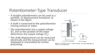
Potentiometer-Type Transducer
11
• Astraight potentiometer can be used as a
position, or displacement transducer as
shown in the figure.
• A shaft is connected to the potentiometer
moving contact or wiper.
• The potentiometer has a supply voltage
(E), and so the position of the wiper
determines the output voltage (Vo).
• The shaft displacement can be measured
electrically and the measurement can be
displayed or transmitted for further
processing.
12.
Potentiometer-Type Transducer
12
• Advantages:
•It can be as large or as small as required
• It can be perfectly linear, thus giving linear sensitivity
• Sensitivity – ratio of output voltage to displacement
• Disadvantages:
• Output voltage changes in steps as the wiper is moved
between potentiometer coils
• The transducer resolution depends upon the number of turns on
the potentiometer winding.
13.
Strain
Gauges
13
• A straingauge uses the resistance change in a wire when it
is strained to measure the physical change that produces
the strain.
• Classified as bonded and unbonded.
• Bonded strain gauge is bonded (glued) on to the physical
quantity under investigation.
• For example, the strain or compression in a metal beam may be
investigated by bonded strain gauge.
• Unbonded strain gauge is normally part of an individual
transducer used to investigate an applied force.
14.
Unbonded Strain Gauges
14
•Figure shows the construction of one type of
unbonded strain gauge.
• Four nickel alloy wires, typically 25μm in
diameter, are tightly stretched between posts on a
metal frame and movable armature.
• An external force, when applied, causes two of the
wires to be positively strained (increased in length)
and the other two wires to be negatively strained
(shortened).
• The lengthened wires show an increase in
resistance and the shortened wires show a
decreased resistance.
• By connecting the wires into a Wheatstone bridge,
the resistance change can be measured and the
force that produced the change can be calculated.
15.
Bonded Strain
Gauges
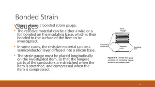
• Figureshows a bonded strain gauge.
• The resistive material can be either a wire or a
foil bonded on the insulating base, which is then
bonded to the surface of the item to be
investigated.
• In some cases, the resistive material can be a
semiconductor layer diffused into a silicon base.
• The strain gauge must be placed longitudinally
on the investigated item, so that the longest
parts of the conductors are stretched when the
item is stretched, and compressed when the
item is compressed.
15
16.
Strain
Gauges
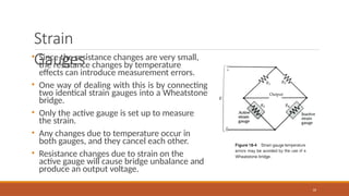
• Since theresistance changes are very small,
the resistance changes by temperature
effects can introduce measurement errors.
• One way of dealing with this is by connecting
two identical strain gauges into a Wheatstone
bridge.
• Only the active gauge is set up to measure
the strain.
• Any changes due to temperature occur in
both gauges, and they cancel each other.
• Resistance changes due to strain on the
active gauge will cause bridge unbalance and
produce an output voltage.
16
17.
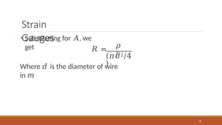
Strain
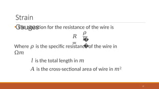
Gauges
• The equationfor the resistance of the wire is
𝑅
=
𝜌
𝑙
17
�
�
Where 𝜌 is the specific resistance of the wire in
Ω𝑚
𝑙 is the total length in 𝑚
𝐴 is the cross-sectional area of wire in 𝑚2
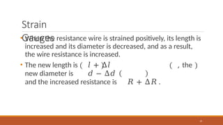
Strain
Gauges
• When theresistance wire is strained positively, its length is
increased and its diameter is decreased, and as a result,
the wire resistance is increased.
• The new length is 𝑙 + Δ𝑙 , the
new diameter is 𝑑 − Δ𝑑
and the increased resistance is 𝑅 + Δ𝑅 .
19
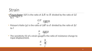
20.
Strain
Gauges
𝐺𝐹
=
• Gauge Factor(GF) is the ratio of Δ𝑅 to 𝑅 divided by the ratio of Δ𝑙
to 𝑙
Δ𝑅/𝑅
Δ𝑙/
𝑙
𝜇
=
• Poisson’s Ratio (𝜇) is the ratio of Δ𝑑 to 𝑑 divided by the ratio of Δ𝑙
to 𝑙
Δ𝑑/𝑑
Δ𝑙/
𝑙
• The sensitivity (S) of a strain gauge is the ratio of resistance change to
input displacement.
𝑆
=
Δ
𝑅
20
Δ
𝑙
21.
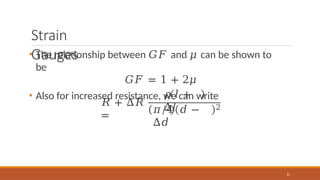
Strain
Gauges
• The relationshipbetween 𝐺𝐹 and 𝜇 can be shown to
be
𝐺𝐹 = 1 + 2𝜇
• Also for increased resistance, we can write
𝑅 + Δ𝑅
=
𝜌 𝑙 +
Δ𝑙
𝜋/4 𝑑 −
Δ𝑑
21
2
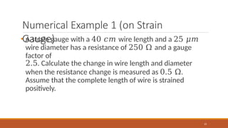
Numerical Example 1(on Strain
Gauge)
23
• A strain gauge with a 40 𝑐𝑚 wire length and a 25 𝜇𝑚
wire diameter has a resistance of 250 Ω and a gauge
factor of
2.5. Calculate the change in wire length and diameter
when the resistance change is measured as 0.5 Ω.
Assume that the complete length of wire is strained
positively.
24.
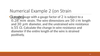
Numerical Example 2(on Strain
Gauge)
24
• A strain gauge with a gauge factor of 2 is subject to a
0.28 𝑚𝑚 strain. The wire dimensions are 50 𝑐𝑚 length
and 30 𝜇𝑚 diameter, and the unstrained wire resistance
is 55 Ω. Calculate the change in wire resistance and
diameter if the entire length of the wire is strained
positively.
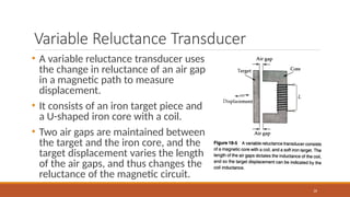
Variable Reluctance Transducer
•A variable reluctance transducer uses
the change in reluctance of an air gap
in a magnetic path to measure
displacement.
• It consists of an iron target piece and
a U-shaped iron core with a coil.
• Two air gaps are maintained between
the target and the iron core, and the
target displacement varies the length
of the air gaps, and thus changes the
reluctance of the magnetic circuit.
26
27.
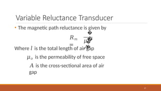
Variable Reluctance Transducer
•The magnetic path reluctance is given by
𝑅𝑚
=
�
�
27
�
�
𝜇
𝐴
Where 𝑙 is the total length of air gap
𝜇𝑜 is the permeability of free space
𝐴 is the cross-sectional area of air
gap
28.
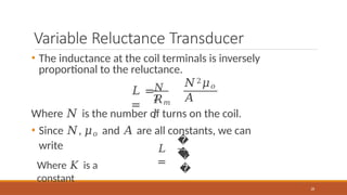
Variable Reluctance Transducer
•The inductance at the coil terminals is inversely
proportional to the reluctance.
𝑁
2
𝐿 =
=
𝑁2𝜇𝑜
𝐴
𝑅𝑚
𝑙
Where 𝑁 is the number of turns on the coil.
• Since 𝑁, 𝜇𝑜 and 𝐴 are all constants, we can
write 𝐿
=
�
�
28
�
�
Where 𝐾 is a
constant
29.
Variable Reluctance Transducer
29
•Since the coil inductance is inversely proportional to the air
gap length, the target displacement can be measured by
monitoring the coil inductance.
30.
Numerical Example 1
(onVariable Reluctance Transducer)
30
• The coil in a variable reluctance transducer has a 1 𝑚𝐻
inductance when the total air gap length is 1 𝑚𝑚. Calculate
the inductance change when the air gap is reduced by 0.2
𝑚𝑚.
31.
Numerical Example 2
(onVariable Reluctance Transducer)
31
• The coil in a variable reluctance transducer has a 0.5
𝑚𝐻 inductance when the total air gap length is 1.3 𝑚𝑚.
The inductance increases to 0.55 𝑚𝐻 when the target is
moved closer to the core. Calculate the movement of the
target.
32.
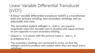
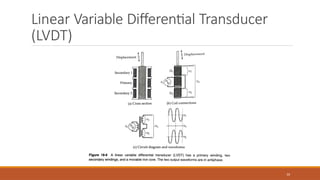
Linear Variable DifferentialTransducer
(LVDT)
32
• A linear variable differential transducer (LVDT) is a transformer
with one primary winding, two secondary windings and an
adjustable iron core.
• The secondary output voltages 𝑣1 and 𝑣2 are equal in
magnitude when the movable core is situated with equal sections
of core opposite to each secondary winding.
• Output 𝑣1 is in phase with the primary input 𝑣𝑖 and 𝑣2 is
in antiphase to 𝑣𝑖.
• The secondary windings are connected in series, so that the
voltages cancel to produce zero output when they are equal and in
antiphase.
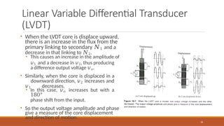
Linear Variable DifferentialTransducer
(LVDT)
34
• When the LVDT core is displace upward,
there is an increase in the flux from the
primary linking to secondary 𝑁1 and a
decrease in that linking to 𝑁2.
• This causes an increase in the amplitude of
𝑣1 and a decrease in 𝑣2, thus producing
a difference output voltage 𝑣𝑜.
• Similarly, when the core is displaced in a
downward direction, 𝑣2 increases and
𝑣1 decreases.
• In this case, 𝑣𝑜 increases but with a
180°
phase shift from the input.
• So the output voltage amplitude and phase
give a measure of the core displacement
and direction of motion.
35.
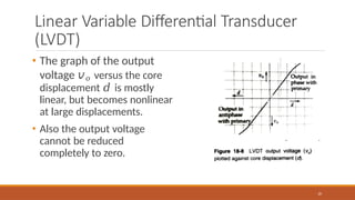
Linear Variable DifferentialTransducer
(LVDT)
• The graph of the output
voltage 𝑣𝑜 versus the core
displacement 𝑑 is mostly
linear, but becomes nonlinear
at large displacements.
• Also the output voltage
cannot be reduced
completely to zero.
35
36.
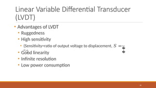
Linear Variable DifferentialTransducer
(LVDT)
• Advantages of LVDT
• Ruggedness
• High sensitivity
�
�
36
• (Sensitivity=ratio of output voltage to displacement, 𝑆 =
𝑣𝑜
)
• Good linearity
• Infinite resolution
• Low power consumption
37.
Linear Variable DifferentialTransducer
(LVDT)
37
• Disadvantages of LVDT
• Relatively large core movements are required to produce a
measurable output
• The core mass limits its dynamic response
38.
Numerical Example 1(on
LVDT)
38
• A 50 𝑚𝑉 output is produced by an LVDT when the core
displacement is 10 𝑚𝑚 from its zero position. Calculate
the core displacement when the output is 35 𝑚𝑉.
39.
Numerical Example 2(on
LVDT)
39
• An LVDT with 0.5 𝑉/𝑚𝑚 sensitivity has its output
amplified by a factor of 50 and applied to a meter which can
display a minimum of 1 𝑚𝑉. Calculate the overall sensitivity
of the system, and determine the minimum detectable core
displacement.
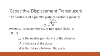
Capacitive Displacement Transducers
•Capacitance of a parallel plate capacitor is given by
𝜀𝑜𝜀𝑟
𝐴
𝐶 =
41
𝑑
Where 𝜀𝑜 is the permittivity of free space (8.84 ×
10−12)
𝜀𝑟 is the relative permittivity of the dielectric
𝐴 is the area of the plates
𝑑 is the distance between the plates
42.
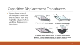
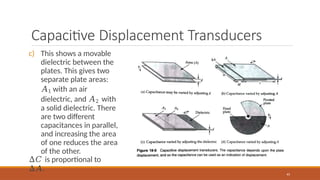
Capacitive Displacement Transducers
•Figure shows several
parallel-plate capacitors
and illustrates how they
might be adjusted when
used in a displacement
transducer.
42
43.
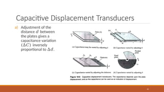
Capacitive Displacement Transducers
a)Adjustment of the
distance 𝑑 between
the plates gives a
capacitance variation
(∆𝐶) inversely
proportional to ∆𝑑.
43
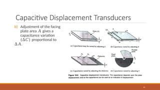
Capacitive Displacement Transducers
c)This shows a movable
dielectric between the
plates. This gives two
separate plate areas:
𝐴1 with an air
dielectric, and 𝐴2 with
a solid dielectric. There
are two different
capacitances in parallel,
and increasing the area
of one reduces the area
of the other.
∆𝐶 is proportional to
∆𝐴.
45
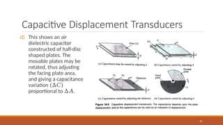
46.
Capacitive Displacement Transducers
d)This shows an air
dielectric capacitor
constructed of half-disc
shaped plates. The
movable plates may be
rotated, thus adjusting
the facing plate area,
and giving a capacitance
variation (∆𝐶)
proportional to ∆𝐴.
46
47.
Capacitive Displacement Transducers
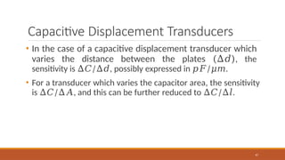
47
•In the case of a capacitive displacement transducer which
varies the distance between the plates (∆𝑑), the
sensitivity is ∆𝐶/∆𝑑, possibly expressed in 𝑝𝐹/𝜇𝑚.
• For a transducer which varies the capacitor area, the sensitivity
is ∆𝐶/∆𝐴, and this can be further reduced to ∆𝐶/∆𝑙.
48.
Numerical Example 1(on Capacitive
Displacement Transducers)
48
• A parallel plate capacitive transducer has a plate area
(𝑙 𝑥 𝑤) = (40𝑚𝑚 𝑥 40𝑚𝑚) and plate spacing 𝑑 =
0.5 𝑚𝑚. Calculate the device capacitance and
displacement (∆𝑑) that causes the capacitance to change
by 5 𝑝𝐹. Also determine the transducer sensitivity.
49.
Numerical Example 2(on Capacitive
Displacement Transducers)
49
• For the capacitive transducer in the previous example,
calculate the change in length (∆𝑙) that produces the
same (5 𝑝𝐹) capacitance change. Also, determine the
new transducer sensitivity.
50.
Numerical Example 3(on Capacitive
Displacement Transducers)
50
• A capacitive transducer is constructed of two half-disc
plates. The plates are 2 𝑚𝑚 apart, and each has an area
of
1.4 × 10⁻³ 𝑚2. Calculate the maximum capacitance,
and the transducer sensitivity in pF/degree.
51.
Capacitive Pressure Transducers
•Figure shows the cross section
of a pressure transducer which
consists of a flat fixed plate and
a plastic diaphragm with a
metal film as a movable plate.
51
52.
Capacitive Pressure Transducers
•This is a capacitive microphone designed to receive sound
waves as a pressure variation on its diaphragm.
• The gap between the plates changes when the diaphragm
is pressured, consequently, the transducer capacitor
changes.
• The capacitance becomes charged to the level of the
supply voltage 𝑒𝐶= 𝐸, so that, in the absence of a
pressure variation, there is no current flow and no resistor
voltage drop (𝑒𝑅).
52
53.
Capacitive Pressure Transducers
53
•The capacitor charge equation is 𝑄 = 𝐶𝐸.
• So as 𝐶 varies with the varying pressure, the charge on 𝐶
must also vary, and this produces a varying current (𝑖) from
the supply.
• The current causes a varying voltage drop across 𝑅 which
can be amplified and further processed.
• The frequency range of this transducer is 40 𝐻𝑧 to 15
𝑘𝐻𝑧, which approximately matches the human hearing
range.
54.
Capacitive Pressure Transducers
54
•Capacitive transducers can be used for measurement of
very small displacements, and they can be much more
sensitive than other transducer types.
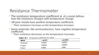
Resistance Thermometer
• Theresistance temperature coefficient 𝛼 of a metal defines
how the resistance changes with temperature change.
• All pure metals have positive temperature coefficient.
• Their resistance increases as the temperature increases.
• Some materials, like semiconductors, have negative temperature
coefficient.
• Their resistance decreases as the temperature increases.
56
57.
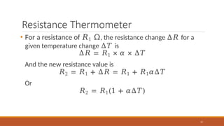
Resistance Thermometer
57
• Fora resistance of 𝑅1 Ω, the resistance change Δ𝑅 for a
given temperature change Δ𝑇 is
Δ𝑅 = 𝑅1 × 𝛼 × ∆𝑇
And the new resistance value is
𝑅2 = 𝑅1 + Δ𝑅 = 𝑅1 + 𝑅1𝛼∆𝑇
Or
𝑅2 = 𝑅1(1 + 𝛼∆𝑇)
58.
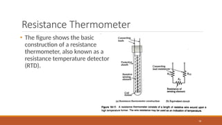
Resistance Thermometer
58
• Thefigure shows the basic
construction of a resistance
thermometer, also known as a
resistance temperature detector
(RTD).
59.
Resistance Thermometer
59
• Theresistive temperature-sensing element, often very pure platinum, is
in the form of a coiled wire held in position inside a protective sheath.
• The sheath may be glass or stainless steel, or any other suitable
material.
• The sensing element wire is wound on a mica former.
• Insulated connecting leads are provided, and these must have a
much lower resistance than the sensing element.
• An RTD is usually connected into a Wheatstone bridge circuit.
• This allows for detection of very small changes in the resistance of
the sensing element, and the meter M used to measure the bridge
unbalance voltage can be calibrated to indicate temperature.
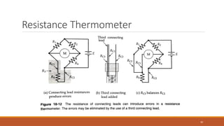
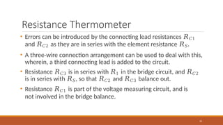
Resistance Thermometer
61
• Errorscan be introduced by the connecting lead resistances 𝑅𝐶1
and 𝑅𝐶2 as they are in series with the element resistance 𝑅𝑆.
• A three-wire connection arrangement can be used to deal with this,
wherein, a third connecting lead is added to the circuit.
• Resistance 𝑅𝐶3 is in series with 𝑅1 in the bridge circuit, and 𝑅𝐶2
is in series with 𝑅𝑆, so that 𝑅𝐶2 and 𝑅𝐶3 balance out.
• Resistance 𝑅𝐶1 is part of the voltage measuring circuit, and is
not involved in the bridge balance.
62.
Resistance Thermometer
62
• Advantages:
•Can be employed over a wide temperature range
• From −200 ℃ to over +650 ℃
• Tough
• Extremely accurate
• Disadvantages
• More expensive
• They need a power supply and bridge
63.
Numerical Example 1
(onResistance Thermometer)
63
• The resistance of a coil of nickel wire is 25 Ω at 20 ℃. This rises
to 37 Ω when the coil has been submerged in a liquid for some
time. Calculate the temperature of the liquid.
64.
Numerical Example 2
(onResistance Thermometer)
64
• A resistance thermometer has a temperature coefficient of 0.0039
at 20 ℃ and a resistance of 130 Ω. Calculate the temperature
when its resistance measures 175 Ω.
65.
Thermistor
65
• A thermistoris a thermally sensitive resistor.
• It is a resistor with important thermal characteristics.
• Most thermistors have a negative temperature coefficient, but
some have positive temperature coefficient.
• Thermistors are widely used in measurement and control of
temperature, liquid level, etc.
66.
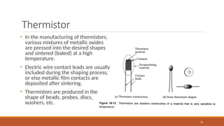
Thermistor
66
• In themanufacturing of thermistors,
various mixtures of metallic oxides
are pressed into the desired shapes
and sintered (baked) at a high
temperature.
• Electric wire contact leads are usually
included during the shaping process,
or else metallic film contacts are
deposited after sintering.
• Thermistors are produced in the
shape of beads, probes, discs,
washers, etc.
67.
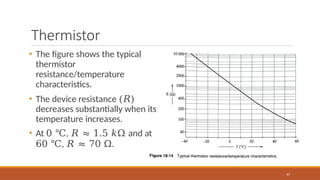
Thermistor
67
• The figureshows the typical
thermistor
resistance/temperature
characteristics.
• The device resistance (𝑅)
decreases substantially when its
temperature increases.
• At 0 ℃, 𝑅 ≈ 1.5 𝑘Ω and at
60 ℃, 𝑅 ≈ 70 Ω.
68.
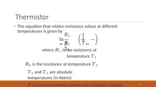
Thermistor
• The equationthat relates resistance values at different
temperatures is given by
𝑅1
ln
= 𝛽
1
1
−
68
𝑅2 𝑇1
𝑇2
where 𝑅1 is the resistance at
temperature 𝑇1
𝑅2 is the resistance at temperature 𝑇2
𝑇1 and 𝑇2 are absolute
temperatures (in Kelvin)
𝛽 is a constant which defines the resistance change
Thermistor
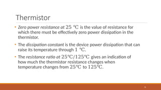
70
• Zero powerresistance at 25 ℃ is the value of resistance for
which there must be effectively zero power dissipation in the
thermistor.
• The dissipation constant is the device power dissipation that can
raise its temperature through 1 ℃.
• The resistance ratio at 25℃/125℃ gives an indication of
how much the thermistor resistance changes when
temperature changes from 25℃ to 125℃.
71.
Thermistor
71
• Advantages:
• Quickresponse
• Good sensitivity
• High resistance
• Less errors
• Low cost
• Small size
• Disdvantages:
• Smaller range
• Non-linear
72.
Numerical Example 1(on Thermistor)
72
• Calculate the resistance of the 300 Ω thermistor at temperatures
of
20 ℃ and 30 ℃.
73.
Numerical Example 2(on Thermistor)
73
• Calculate the resistance of the 30 𝑘Ω thermistor at 50
℃.
74.
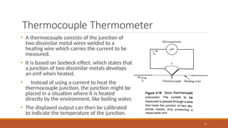
Thermocouple Thermometer
74
• Athermocouple consists of the junction of
two dissimilar metal wires welded to a
heating wire which carries the current to be
measured.
• It is based on Seebeck effect, which states that
a junction of two dissimilar metals develops
an emf when heated.
• Instead of using a current to heat the
thermocouple junction, the junction might be
placed in a situation where it is heated
directly by the environment, like boiling water.
• The displayed output can then be calibrated
to indicate the temperature of the junction.
75.
Thermocouple Thermometer
75
• Advantages:
•Ruggedness
• Relatively inexpensive
• Usable over a wide range of temperature (from −200℃ to
+2800℃)
• Disadvantages:
• Low-level output (requires amplification)
• Lower accuracy
76.
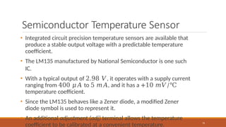
Semiconductor Temperature Sensor
76
•Integrated circuit precision temperature sensors are available that
produce a stable output voltage with a predictable temperature
coefficient.
• The LM135 manufactured by National Semiconductor is one such
IC.
• With a typical output of 2.98 𝑉, it operates with a supply current
ranging from 400 𝜇𝐴 to 5 𝑚𝐴, and it has a +10 𝑚𝑉/℃
temperature coefficient.
• Since the LM135 behaves like a Zener diode, a modified Zener
diode symbol is used to represent it.
• An additional adjustment (adj) terminal allows the temperature
coefficient to be calibrated at a convenient temperature.
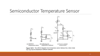
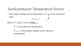
Semiconductor Temperature Sensor
•The output voltage at any temperature (𝑇2) can be calculated
from
𝑉𝑜(𝑇2) =
𝑉𝑜(𝑇1)
𝑇
2
×
78
𝑇
1
Where 𝑇1 and 𝑇2 are in Kelvin
𝑇1 is the reference temperature
𝑉𝑜(𝑇1) is the output voltage at the reference
temperature
79.
Semiconductor Temperature Sensor
79
•For calibration, a potentiometer is connected in parallel with the output,
and its moving contact is connected to the adj terminal.
• The use of a constant current source also helps ensure a stable
temperature coefficient.
• The LM139 (𝑍1) is a Zener diode providing a constant voltage to
𝑅2, regardless of supply voltage variations.
• Thus, there is a constant voltage drop across 𝑅2, resulting in a
constant current through LM135 (𝑍2).
80.
Semiconductor Temperature Sensor
80
•The LM135 operates over a temperature range of −55℃ to
+150℃.
• Its output voltage can be processed to indicate the temperature of its
environment.
• It can also be used together with a voltage level detector, to control a
heater.
• For example, by switching it ON when air temperature drops below a given
point, and switching OFF again when the temperature rises to the desired
level.
Light
Units
• The totallight energy output, or
luminous flux (𝜙𝑠), from a source can
be measured in milliwatts (𝑚𝑊) or
in lumens (𝑙𝑚).
• 1 𝑙𝑚 = 1.496 𝑚𝑊
• The luminous intensity (𝐸𝑠), or
illuminance of a light source is defined
as the luminous flux density per unit
solid angle emitting from the source.
• It is measured in candelas (𝑐𝑑), where one
candela is equal to one lumen per unit solid
angle (assuming a point source that emits
light evenly in all directions).
𝜙
𝑠
82
𝐸𝑠 =
4𝜋
83.
Light
Units
• The lightintensity (𝐸𝐴) on an area at a given distance from the source
is determined from the surface area of a sphere surrounding the
source.
• At a distance of 𝑟 meters, the luminous flux is spread over a spherical
area of
4𝜋𝑟2 square meters.
• Therefore, �
�
𝐸
=
𝜙
𝑠
83
4𝜋𝑟
2
• When the total flux is expressed in lumens, this equation gives the luminous
intensity in lumens per square meters (𝑙𝑚/𝑚2), also termed lux (𝑙𝑥)
• The luminous intensity can also be measured in milliwatts per square
centimeter (𝑚𝑊/𝑐𝑚2) or lumens per square foot (𝑙𝑚/𝑓𝑡2), also known
as a foot candle (𝑓𝑐)
• 1 𝑓𝑐 = 10.764 𝑙𝑥
84.
Light
Units
84
• Light energyis electromagnetic radiation.
• It is in the form of electromagnetic wave.
• So it can be defined in terms of frequency and wavelength, as well as
intensity.
• Wavelength, frequency and velocity are related by the equation
𝑐 = 𝑓𝜆
where 𝑐 = velocity = 3 × 10⁸ 𝑚/𝑠 for electromagnetic waves
𝑓 = frequency in 𝐻𝑧
𝜆 = wavelength in 𝑚
85.
Numerical Example onLight Units
85
• Calculate the light intensity 3 𝑚 from a lamp that emits 25 𝑊 of light
energy. Determine the total luminous flux striking an area of 0.25 𝑚2
at 3 𝑚 from the lamp.
86.
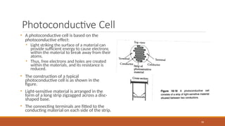
Photoconductive Cell
• Aphotoconductive cell is based on the
photoconductive effect:
• Light striking the surface of a material can
provide sufficient energy to cause electrons
within the material to break away from their
atoms.
• Thus, free electrons and holes are created
within the materials, and its resistance is
reduced.
• The construction of a typical
photoconductive cell is as shown in the
figure.
• Light-sensitive material is arranged in the
form of a long strip zigzagged across a disc-
shaped base.
• The connecting terminals are fitted to the
conducting material on each side of the strip.
86
87.
Photoconductive Cell
87
• CadmiumSulfide (CdS) and Cadmium Selenide (CdSe) are the two
materials normally used in photoconductive cells.
• Both respond slowly to changes in light intensity.
• The response time (𝑡𝑟𝑒𝑠) for cadmium selenide is about 10 𝑚𝑠
and for cadmium sulfide, it is about 100 𝑚𝑠.
• Cadmium selenide has larger temperature sensitivity compared to
cadmium sulfide.
88.
Photoconductive Cell
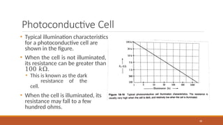
88
• Typicalillumination characteristics
for a photoconductive cell are
shown in the figure.
• When the cell is not illuminated,
its resistance can be greater than
100 𝑘Ω.
• This is known as the dark
resistance of the
cell.
• When the cell is illuminated, its
resistance may fall to a few
hundred ohms.
89.
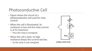
Photoconductive Cell
• Figureshows the circuit of a
photoconductive cell used for relay
control.
• When the cell is illuminated, its
resistance is low and the relay current
is at its maximum.
• Thus the relay is energized.
• When the cell is dark, its high
resistance keeps the current too low.
• So the relay is not energized.
89
90.
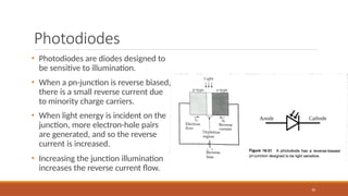
Photodiodes
• Photodiodes arediodes designed to
be sensitive to illumination.
• When a pn-junction is reverse biased,
there is a small reverse current due
to minority charge carriers.
• When light energy is incident on the
junction, more electron-hole pairs
are generated, and so the reverse
current is increased.
• Increasing the junction illumination
increases the reverse current flow.
90
91.
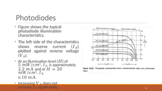
Photodiodes
• Figure showsthe typical
photodiode illumination
characteristics.
• The left side of the characteristics
shows reverse current (𝐼𝑅)
plotted against reverse voltage
(𝑉𝑅).
• At an illumination level (𝐻) of
5 𝑚𝑊/𝑐𝑚2, 𝐼𝑅 is approximately
2.2 𝑚𝐴 and at 𝐻 = 20
𝑚𝑊/𝑐𝑚2, 𝐼𝑅
is 10 𝑚𝐴.
• Increasing 𝑉𝑅 does not
increase 𝐼𝑅 significantly. 91
92.
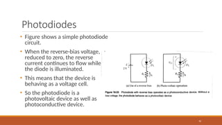
Photodiodes
92
• Figure showsa simple photodiode
circuit.
• When the reverse-bias voltage,
reduced to zero, the reverse
current continues to flow while
the diode is illuminated.
• This means that the device is
behaving as a voltage cell.
• So the photodiode is a
photovoltaic device as well as
photoconductive device.
93.
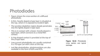
Photodiodes
• Figure showsthe cross-section of a diffused
photodiode.
• A thin, heavily doped p-type layer is situated at
the top, where it is exposed to incident light.
• The junction depletion region deeply penetrates
into the lightly doped n-type layer.
• This is in contact with a lower, heavily doped n-
type layer, which connects to a metal film
contact.
• A ring-shaped contact is provided at the top of
the p-type layer.
• Low-current photodiodes are usually contained
in a TO-type can with a lens at the top.
• Just like photodiodes, phototransistors are also
available in the form of BJTs and FETs.
93
94.
Photomultiplier
94
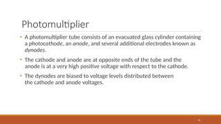
• A photomultipliertube consists of an evacuated glass cylinder containing
a photocathode, an anode, and several additional electrodes known as
dynodes.
• The cathode and anode are at opposite ends of the tube and the
anode is at a very high positive voltage with respect to the cathode.
• The dynodes are biased to voltage levels distributed between
the cathode and anode voltages.
Photomultiplier
96
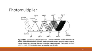
• Radiation strikingthe photocathode imparts energy to electrons within
the cathode surface material, causing them to be emitted.
• The positive voltage on the dynode 1 accelerates the electrons from the
cathode toward the dynode.
• The dynode surface material facilitates secondary emission and the
number of secondary electrons exceeds the number of primary electrons
from the cathode.
• The secondary electrons emitted from dynode 1 are accelerated toward
the more positive dynode 2, where further increased secondary emission
is produced.
97.
Photomultiplier
97
• The processof increasing levels of secondary emission continues
between successive dynodes until the electrons arrive at the
anode, where they are collected.
• The number of electrons arriving at the anode far exceeds the
number emitted from the cathode.
• So, the original electrons have been multiplied, or in other words the
photoemission current has been amplified.
• Current amplifications of the range of 107 are possible depending on
the number of dynodes and the applied voltage levels.
98.
Photomultiplier
98
• The typicalphotomultiplier tube
characteristics in the figure shows anode
currents ranging approximately from 1
mA to 4 mA for incident light levels of 25
to 100 microlumens.
• The dark current occurs when the
cathode is not illuminated.
• The anode current is directly
proportional to the incident illumination
level.
• The phototomultiplier tube is extremely
sensitive and are appropriate for the
detection of fast, low-level occurrences.
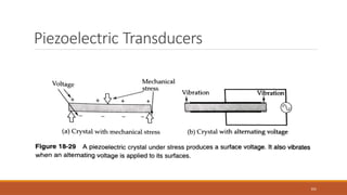
Piezoelectric Transducers
101
• Ifa mechanical stress is applied to a wafer of quartz crystal, a voltage
proportional to the stress appears at the surfaces of the crystal.
• When the stress is removed, the voltage disappears.
• The crystal also vibrates, or resonates, when an alternating voltage with
the natural resonance frequency of the crystal is applied to its surfaces.
• The materials that exhibit this behaviour are called piezoelectric
materials.
• Since the crystal resonance frequency is extremely stable, piezoelectric
crystals are widely used to stabilize the frequency of oscillators.
• They are also used in pressure transducers.
Piezoelectric Transducers
103
• Piezoelectricwafers cut from quartz and other natural materials are
limited in shape and thus limited in applications.
• Synthetic piezoelectric devices can be manufactured in almost any
desired shape.
• The manufacture of synthetic piezoelectric devices involves pressing
powdered ceramic material, such as barium titanate, into require
shapes, the firing it at high temperatures while subjected to a high direct
electric field.
• The high voltage aligns the atomic structure of the material into a
shape that can produce the piezoelectric effect.
104.
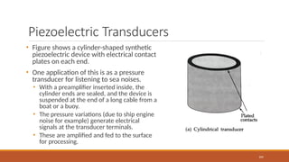
Piezoelectric Transducers
• Figureshows a cylinder-shaped synthetic
piezoelectric device with electrical contact
plates on each end.
• One application of this is as a pressure
transducer for listening to sea noises.
• With a preamplifier inserted inside, the
cylinder ends are sealed, and the device is
suspended at the end of a long cable from a
boat or a buoy.
• The pressure variations (due to ship engine
noise for example) generate electrical
signals at the transducer terminals.
• These are amplified and fed to the surface
for processing.
104
105.
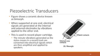
Piezoelectric Transducers
• Figureshows a ceramic device known
as bimorph.
• When supported at one end, electrical
signals are generated at the internal
and external electrodes by vibrations
applied to the other end.
• This is used in record player cartridge.
• The minute vibrations generated as the
stylus moves in a record track are
converted into electrical signals which
are then amplified and applied to
speakers.
105
106.
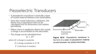
Piezoelectric Transducers
• Apiezoelectric transducer is basically a layer
of crystal material between two metal plates.
• Since the crystal material is a dielectric, the
device has a capacitance that can be
calculated from its dimensions and relative
permittivity.
• When a force is applied to distort the crystal,
a charge is accumulated on the electrodes.
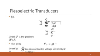
• The charge can be calculated from
𝑄 = 𝑑𝐹
where 𝑄 is charge in coulombs
𝑑 is charge sensitivity in 𝐶/𝑁
𝐹 is the force in newtons
106
107.
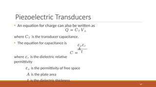
Piezoelectric Transducers
• Anequation for charge can also be written as
𝑄 = 𝐶𝑇 𝑉𝑜
where 𝐶𝑇 is the transducer capacitance.
• The equation for capacitance is 𝜀𝑜𝜀𝑟
𝐴
𝐶 =
107
𝑡
where 𝜀𝑟 is the dielectric relative
permittivity
𝜀𝑜 is the permittivity of free space
𝐴 is the plate area
𝑡 is the dielectric thickness
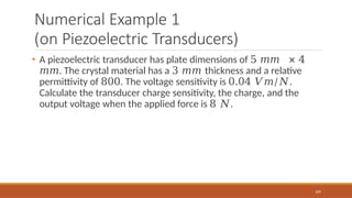
Numerical Example 1
(onPiezoelectric Transducers)
109
• A piezoelectric transducer has plate dimensions of 5 𝑚𝑚 × 4
𝑚𝑚. The crystal material has a 3 𝑚𝑚 thickness and a relative
permittivity of 800. The voltage sensitivity is 0.04 𝑉𝑚/𝑁.
Calculate the transducer charge sensitivity, the charge, and the
output voltage when the applied force is 8 𝑁.
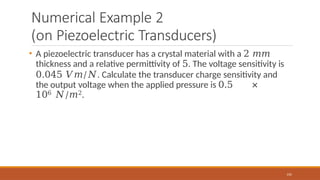
110.
Numerical Example 2
(onPiezoelectric Transducers)
110
• A piezoelectric transducer has a crystal material with a 2 𝑚𝑚
thickness and a relative permittivity of 5. The voltage sensitivity is
0.045 𝑉𝑚/𝑁. Calculate the transducer charge sensitivity and
the output voltage when the applied pressure is 0.5 ×
106 𝑁/𝑚2.
111.
References
111
• David A.Bell, “Electronic Instrumentation and Measurements”, 3rd
Edition, Oxford University Press, 2013


![Lesson[1] .pdf input transduder notes](https://cdn.slidesharecdn.com/ss_thumbnails/lesson1-240610175041-c8777e45-thumbnail.jpg?width=640&height=640&fit=bounds)


![[Deck] What's New in Spark-Iceberg Integration via DSV2.pptx](https://cdn.slidesharecdn.com/ss_thumbnails/deckwhatsnewinspark-icebergintegrationviadsv2-260210005337-25955b12-thumbnail.jpg?width=640&height=640&fit=bounds)


