SlideShare a Scribd company logo
1 of 217
Download to read offline
14/09/2023 1
L15 and 16_Laser, Electron, Plasma and Ion Beam Machining
Micro Electro-Mechanical System (MEMS)
Fabrication
Dr. Poonam Sundriyal
Assistant Professor
Department of Mechanical Engineering
IIT Kharagpur
14/09/2023 2
LASER Beam Machining (LBM)
Focusing Solar radiation on a paper
Intensity of sun at earth’s surface = 1 kW/m2
Focusing Light radiation on workpiece
Laser power density = 1.9x10⁷ kW/m2
• Can melt all the materials (including diamond)
• Spontaneous absorption
• Spontaneous emission
• Stimulated emission
Laser interaction with an Atom
A. Spontaneous
absorption
B. Spontaneous
emission
LEL
HEL
LEL: Lower energy level/ Ground state, HEL: Higher energy level/ Excited state
: electron , : energy photons,
14/09/2023 3
Light Amplification by Stimulated Emission of Radiation
HEL2
HEL1
C. Stimulated
emission
parent
stimulated
14/09/2023 4
Major Applications
➢ Photolithography
➢ Laser Cutting of Metal Sheets, Paper, Glass, Plastics,
Textiles, Rubber, Ceramic, etc.
➢ Laser Micro-welding.
➢ Laser scribing, marking, engraving
Applications of Laser in MEMS
LaserForming
➢ Laser Surface Cladding
➢ Laser Rapid Manufacturing
➢ Laser polymerization
➢ Laser Metal Forming
➢ Laser Surface Alloying
LaserScribing
LaserCladding
LaserRapidPrototyping
14/09/2023
Characteristics of LASER
1. Lasers are monochromatic: they have single
output wavelength or a pure color with an extremely
narrow bandwidth.
• Depending on the laser type, they can have
wavelength from ultraviolet through visible and
even in the infrared portion of the electromagnetic
spectrum.
• Wavelength selection is important dependent on the
material being processes. Analysis of objects at a
certain energy is important for research purpose.
Red (660 & 635 nm), green (532 & 520 nm) and blue-violet (445 & 405 nm) lasers
3. Lasers are highly directional/ low divergence
• Lasers have been bounced off the moon to
accurately measure the distance between moon
and earth.
LED
2. Highly coherent: all waves are exactly in
phase with one another.
Light bulb
5
14/09/2023 6
Laser cutting dominants the industrial laser applications & has more than 75% of share of all LM
applications.
• Fast cutting with higher quality than other competing processes.
Basic Principle : Melting with a focused laser beam and molten material ejection by a high-pressure gas
jet.
• Excimer Laser, NdYAG & Fiber Lasers
• Laser Power = 500-5000W
• Focal spot size ~ 0.1 – 0.3 mm
• Power density of 1kW power at focal spot of 0.3mm ~ 1.4 X10⁶ W/cm2
• Effect on material
* Melting
* Vaporization
• Pressurized co-axial gas jet ejects the molten / vaporized material
Laser Cutting
14/09/2023 7
Energy balance equation: No conduction loss
P = w.t.v. (Cp.Tm + Lf + m’Lv)
In cutting, m’ =0
Cutting speed, v = P / {w.t. (Cp.Tm + Lf )}
P/v.t = w. (Cp.Tm + Lf ) /  = S, Constant
for a constant w & a given material
Called as “Severance Energy” in (J/mm2)
where,
 = (1-R) Laser Power Coupling
coefficient,
R = Reflectivity of job material
P = Laser power,
t = Sheet thickness,
w = cut or kerf width,
v = cutting speed,
Lf = latent heat of fusion,
Lv = latent heat of vaporization,
m’=Fraction of metal evaporated,
 = density,
T = Temperature raise,
Cp = Specific Heat,
Energy balance in Laser Cutting
w
t
v
Energy required for cutting (Ecutting) = Ereaching
to melting temperature from ambient temp + Ephase change from
solid to liquid + Ephase change from liquid to vapour
(mass flow rate (ṁ) = density * area *
velocity)
Moving laser for cutting
14/09/2023 8
Drilling with Long and Ultra-short Laser Pulses
• Longer pulses continuously heat the material during
the pulse duration.
• Heat conduction: HAZ, recast layer, microcracks.
• Ultrashort laser pulses : a few ps or below
• Due to the extremely short pulse duration, only
electrons are heated at first.
• Energy transfer to the lattice takes place on a
timescale longer than the pulse itself. - Heat
conduction is limited.
• This finally leads to ablation within a well-defined
region with minimum thermal and mechanical
damage to the surrounding
14/09/2023 9
z
a
Energy balance consideration in Laser Beam Drilling
Energy required for drilling (Edrilling) =
Ereaching to vaporization temperature from ambient temp
+ Ephase change from solid to liquid + Ephase change
from liquid to vapour
(mass = density * volume)
Laser position - fixed
Characteristics CO2 Laser Nd:YAG Laser Diode Lasers Excimer Lasers Fiber Laser
Wavelength m 9.6-10.6 1.06 0.8-1.0 0.193-0.354 1.06
Laser power, CW
Pulse energy
Upto 45 kW
1-20 J
50W- 2kW
1-100J
Up to 4kW --Avg.1kW
1-10J,
10kW
Efficiency % 10-15 2–20 20-40 2-3 30
Beam Diverg. 1-3 mr. 1 – 25 mr. 1x200 mr 2 – 6 mr. 1-2 mr.
Beam Transportation Reflecting mirrors Optical fibers Optical fibers Optical fibers Optical fibers
Absorption in metals Low
~2-15%
Moderate
~5-30%
Moderate
~5-30%
High
50%
Moderate
~5-30%
Life, CW (Hrs.)
Pulsed (Shots)
~ 1000s.
~106
~200 Life of
~106 lamps
~ 1000s. 104-107
(one gas fill)
Size of lasers Large Moderate Compact Moderate Compact
Maintenance intervals
(Hr)
1000-2000 500-1000 5,000-10,000 500-1000 5,000-10,000
Mode of operation CW & Pulsed:
ms- sub-s
CW & Pulsed: ms-
Sub-ps
CW &
Modulated
Pulsed
10’s ns
CW & Pulsed:
ms- Sub-ps
14/09/2023 10
Lasers for Material Processing Applications and their Characteristics
14/09/2023 11
Electron Beam Machining (EBM)
• Electron beam is used for machining.
• Electrons are generated by thermionic emission from hot tungsten cathode.
• Thermionic emission : emission of electrons from an electrode due to its temperature.
thermal energy provided to the charge carrier > work function of the material (binding potential).
Fig. Schematic of thermionic emission process
LEL
HEL
LEL: Lower energy level/ Ground state, HEL: Higher energy level/ Excited state
: electron , : energy,
-ve
+ve
14/09/2023 12
• Spot diameter: 10- 200 µm and Power density = 6500 billion W/mm2 = 6.5 × 10¹⁸ W/mm2
• Any material can rapidly melt and vaporize.
• EBM is a very precise vaporization process.
• Basic Process: EBM - Thermal process, similar to LBM. (done in vacuum)
Material-heating: Striking of high-velocity electrons with workpiece.
Kinetic energy of electrons Heat Rapid melting and vaporizing
Electron Beam Machining (EBM)
• Applications: Mask Fabrication for Photolithography, Imaging, Drilling fine holes,
cutting narrow slots, welding, and rapid manufacturing.
14/09/2023 13
Rotating shutter
Electron beam gun: Electrons are generated by
thermionic emission from hot tungsten cathode.
In E-beam gun for cutting & drilling applications, there
is a grid between anode & cathode on which negative
voltage is applied to pulse / modulate the e-beam.
Components of Electron Beam Machining
Power supply: Up to 150 kV, Current : 150 µA-
1.5A.
Vacuum-chamber: 10-4-10-6 Torr (1 Torr = 1
mm Hg) achieved by rotary pump backed
diffusion pump.
Vacuum compatible CNC workstation
Mode of E-beam Operation:
For drilling and cutting - Pulsed electron beam
Single pulse : A single hole in thin sheet;
Multiple pulses: To drill in a thicker material.
For welding : DC electron beam
Parameters so chosen that loss of material due to
vaporization is minimum.
14/09/2023 14
Mechanism of Electron Beam Machining (EBM)
Depth of penetration:
δ = 2.6 x10
-17
(V
2
/ρ) mm
where,
V=Accelerating voltage (Volts) and
ρ = Material density (kg/mm3)
Figure: Movement of an electron below surface
* Unaffected zone: Transparent layer
* Energy of Electrons Lattice of material through collisions.
* Energy transfer Function of kinetic energy or accelerating
voltage.
• Maximum rise in temperature- At a certain depth, not at the
surface, unlike laser heating.
Change in Kinetic Energy of Electron = me(u - uo)2/2 eV, u (km/s) ~ 600√(V)
me= 9.1x10⁻³¹kg, e =1.6 x10⁻¹⁹ Coulomb.
KE is dissipated in the impinging material.
Power requirement for machining:
P = CQ
where,
C = Constant of proportionality or specific power consumption in
EBM , and Q = Material removal rate
14/09/2023 15
Q. What will be the penetration depth of the electron beam accelerated at 150 kV impinging in steel having
density of 76 × 10-7 kg/mm3?
Numerical
Solution: δ = 2.6 x10
-17
(V
2
/ρ) mm
δ = 77 µm
Q. An electron beam of 5 kW power is used for cutting a 150 µm wide slot in 1 mm thick tungsten sheet. Determine the
cutting speed?
(Specific power consumption in EBM (constant of proportionality) for tungsten is 12 W/mm3/min)
Solution: P = CQ
Let the speed of cutting be V mm/min.
Q = AV = 150 × 10-3 × 1 × V mm3/min
P = CTungusten Q
5000 = 12 × 150 × 10-3 × 1 × V
V = 2778 mm/min = 4.6 cm/sec
Source: Intel
Mask Fabrication using Electron Beam Machining
14/09/2023 17
1. Localized heating of work-piece: On an organic or synthetic
backing
* E-beam focal spot diameter ≤ Desired diameter
* Power density : ~108 W/cm2, sufficient to melt & vaporize any material.
2. Vaporization of a small fraction of melted material
• Recoil pressure of escaping vapour pushes the molten material aside
creating a hole.
3. E-beam penetrates in till it reaches the bottom surface of
work piece.
4. Removal of material: As e-beam strikes the auxiliary support
volume in contact is totally vaporized resulting in the explosive
release of backing material vapour
* High velocity vapour carries along with it the molten walls of the capillary,
creating a hole in the work piece and a small cavity in the backing material.
Electron Beam Drilling Process: Four Stages
14/09/2023 18
Energy Balance in EBM
Energy balance considering the kerf will be governed by Thermal Diffusion length ( ddif = 2√(ατ)) as the E-beam spot
size is usually smaller than ddif.
ηP = w.t.v.ρ.Cp. ∆T
w= kerf width ≈ Thermal diffusion length ≈ 2 ατ = 2 α𝑑/𝑣
Where, η =E- beam power coupling efficiency including conduction loss ≈ 0.1,
P = E-beam power in W;
t= depth of penetration in m up to which rise in temperature is ∆ T,
α = Thermal diffusivity = k/ ρ. Cp
k= Thermal conductivity of material in W/mºC
ρ =Material density in g/m3;
Cp = Specific heat in J/kg. ºC;
τ = E-beam material interaction time
(For continuous e-beam scanned at velocity, v interaction time, τ = d/v )
d= width of e-beam in m;
v= Processing speed in m/s
14/09/2023 19
Plasma Arc Manufacturing (PAM)
What is Plasma?
• This is the 4th state of matter – Ionized gas (Electrically
conducting and responsive to magnetism)
• Electrically neutral -numbers of negative charge (electron +
negative ions) and positive charge equal.
Ex: Ionized air (plasma)
What is an Arc?
• An electric arc is a discharge of electric current across a
gap in a circuit.
• An arc discharge is characterized by a low voltage and
relies on thermionic emission of electrons from the
electrodes supporting the arc.
-It can be sustained by plasma.
Electric arc
14/09/2023 20
Introduced in 1957.
Similar to Gas Tungsten Arc Welding (GTAW): Electric Arc is formed
between an electrode and work piece.
Key difference from GTAW:
• In PAW electrode placed in the torch and arc is infused with gas.
• Plasma arc separated from shielding gas
• Plasma forced through a fine-bore copper nozzle : Constricts the arc and
the plasma exits the orifice at high velocities and high temperature ~
20,000 °C.
Plasma transfers the electric arc to the work piece.
Metal to be welded is melted by the intense heat of the arc and fuses together.
Higher energy concentration : Deeper and narrower welds and Increased
welding speed.
Plasma Arc Welding (PAW)
Fig. Schematic of TIG
Fig. Schematic of PAW
14/09/2023 21
Operating Modes in PAW
Micro-plasma: 0.1 to 15 A
PAW was first developed for low current welding of thin materials (less than 0.1 mm thickness) since TIG could not
provide stable arc at low currents.
Micro-plasma arc can be operated at very low welding currents.
• Widely used in electronics industries to weld thin sheets of all materials.
Medium current: 15 to 100 A.
Process characteristics of the plasma arc are similar to the TIG arc, however because plasma is constricted, arc is more
concentrated, thus is capable to weld faster & better than TIG .
• deeper penetration (from higher plasma gas flow), greater tolerance to surface contamination (the electrode is
within the body of the torch) and better tolerance to variations in standoff distance. (up to 2.4 mm thickness)
• Welding of thin film (foil thickness) materials: Most applications of plasma welding are in the low-current range,
from 100 amperes or less.
Room Temperature Plasma
• Surface cleaning
• Surface modification using oxygen, nitrogen, etc.
• Surface adhesion improvement – Important for coating and additive
processing.
• Change of wettability.
• Etching
https://plasmatreatment.co.uk/knowledge-base/videos
14/09/2023 23
Ion Beam Machining (IBM) - Nanofabrication
• A type of particle beam consisting of ionized atoms i.e.
ions.
Sputtering:
• A stream of ions of an inert gas, such as argon or metal
such as gallium is accelerated in a vacuum by high
energies and directed toward a solid workpiece.
• Ion beam knocks off atoms from workpiece by
transferring kinetic energy and momentum to atoms on
the targeted surface. Fig. Schematic of sputtering process
Kinetic Energy> Binding Energy
Ion
atoms
14/09/2023 24
Why IBM is better for Nanomanufacturing
14/09/2023 25
• In a Liquid metal ion source (LMIS), a metal (typically gallium) is
heated to the liquid state and provided at the end of a capillary or a
needle. (Tm= 29.8 º
C)
• An electric field (108 V/cm) is applied to the end of the wetted tip
that causes the liquid Ga to form a point source (2-5 nm tip) in the
shape of “Taylor cone”.
• Conical shape forms because of electrostatic and surface tension
force balance.
• An extraction voltage (negative) pulls Ga from the tip and
efficiently ionizes it by field evaporation of the metal at the end of
the Taylor cone.
Liquid Metal Ion Source (LMIS)
-ve
14/09/2023 26
Most commonly used in Liquid Metal Ion Source because of the following characteristics:
1. Low Ionization Potential of Ga = 6eV
2. Low melting (Tm= 29.8 º
C) minimizes any reaction or inter-diffusion between liquid and tungsten needle substrate.
3. Low volatility at melting point conserves the supply of metal and yields a long source life
4. Good viscous property; no drop off
5. Excellent mechanical, electrical and vacuum properties
Why Gallium?
14/09/2023 27
• A Vacuum system and chamber
• A liquid metal ion source (LMIS)
• An ion column for milling and deposition
• A precision Goniometer stage for sample mounting and
manipulation
• Imaging detectors
• A gas injection system to spray a precursor gas on the
sample surface
• An electron column for imaging
• Scan generators for ions and electrons
• Computer control
Components of FIB system
Beam energy ~ 30 or 50 keV
Beam current ~1 to 20 nA,
Best image resolution ~5 -7 nm, and
Vacuum Chamber pressure ~ 10
-7
mbar
14/09/2023 28
Sputtering rate as the depth of surface layer sputtered per unit time:
V(nm/s) = 0.1 S (M/d) J. Cosθ
where, S -sputtering yield (atoms/ion), M -atomic (molecular) weight (g) of target, d -target density (g/cm3),
J -ion current density (mA/cm2) and θ -angle of incidence
• Only ~5% of ion energy spent for sputtering, 95% is scattering in other processes, mainly heating the target.
• However, the power density on the surface of target = 0.6 W/cm2, so the target will be heated less (usually up to 50-
90 ºC).
• One of the main advantages of ion beam treatment -we can work with a lot of temperature sensitive materials!
Sputtering Yield in IBM
• Sputter yield depends on the energy of the incident ions, angle of incidence on the
surface of work-piece, masses of ions and target atoms, and the binding energy.
Sputter Yield, S = No. atoms removed / No. of striking Ions
14/09/2023 29
Basic Operating Modes in IBM
• Emission of secondary ions and electrons
FIB Imaging (Low ion current)
✓Sputtering of substrate atoms
• FIB Milling (High ion current)
✓Chemical interactions (Gas assisted)
• FIB Deposition
• Implantation
• Enhanced Etching
Imaging
Milling
Deposition
Implantation
14/09/2023 30
Focused Ion Beam (FIB) Setup
14/09/2023 31
FIB Milling
Typical material removal rate is about 1 m3
per second.
• In FIB milling, typically a gallium (Ga) primary ion beam hits the sample
surface and sputters away a small amount of material.
• If the ion energy is adequate the collision can transfer sufficient energy to
the surface atom to overcome its surface binding energy ( 3.8 eV for Au
and 4.7 eV for Si).
• At high primary currents, material can be efficiently removed from the
sample surface, allowing precision milling of the sample with achievable
feature sizes of well below 1 µm.
• At the same time, the sample can be imaged with very high precision.
Note: There are other variants of the process like Reactive Ion Etching (RIE)
where chemical species are incorporated, and the process proceeds chemically.
14/09/2023 32
FIB Deposition
For FIB induced deposition, the necessary processes are:
• Adsorption of the chemical precursor gas onto the sample
surface.
• Decomposition of gas molecules into volatile and non-volatile
products by focused ion beam.
3 dimensional nanostructures can be fabricated using layer
by layer deposition.
Precursor must have two properties, namely :
• Sufficient sticking probability to stick to a surface of interest in sufficient quantity.
• Decompose more rapidly than it is sputtered away by the ion beam.
14/09/2023 33
• Etching / Milling of all material, Reactive etching, Substrate cleaning:
Subtractive
• Deposition: Sputter deposition - Additive
• Ion- beam Lithography – Pattern transfer
• Ion-beam implantation – Doping
Applications of Ion Beam Machining
14/09/2023 34
Applications of Ion Beam Machining
STM Tips
SAMPLE COURTESY UNIVERSITY ROUEN
Coil 700 nm pitch, 80 nm line
width, diamond like amorphous
carbon, Fabricated by FIB
induced deposition
50 nm size holes
patterned on a thin
film using IBM
Deposition and
machining using FIB
14/09/2023 35
Thank You!
14/11/2023 1
L17_Biomimetic for MEMS Fabrication
Micro Electro-Mechanical System (MEMS)
Fabrication
Dr. Poonam Sundriyal
Assistant Professor
Department of Mechanical Engineering
IIT Kharagpur
Manufacturing of Biomimetic Materials/ Surfaces and Devices
https://www.nature.com/arti
cles/s41427-021-00322-y
14/11/2023 3
Biomimicry
Nagel, Ph. D. Dessertation, 2011
https://www.researchgate.net/publication/45812610_Systematic_design_of_biologically-inspired_engineering_solutions
• Meaning: To imitate life.
• Design inspired by nature.
• Biomimicry Inspired by Nature (1997):
Book by Janine Benyus.
• Biomimicry is an approach to innovation
that seeks sustainable solutions to human
challenges by emulating nature’s time-
tested patterns and strategies.
Antibacterial Surface
Self-cleaning
Adhesion
Heat Transfer Optical
Biomimicking: Self cleaning (Hydrophobic) Surfaces
• The Lotus Effect: The surface of
lotus leaves are bumpy, and this
causes water to bead as well as to
pick up surface contaminates in the
process.
• The water rolls off, taking the
contaminates with it.
• Self cleaning surfaces.
• Application in solar cell, fabrics,
healthcare.
https://link.springer.com/content/pdf/bfm:978-3-7643-8321-3/11/1.pdf
https://phys.org/news/2016-06-lotus-leaf-scientists-world-self-cleaning.html
Replication Methods: Micro Replication Double Inversion (MRDI)
https://doi.org/10.1002/admi.201701052
14/11/2023 7
Structural Color – useful for photonics
• Structure design is responsible for color,
not pigments – environment friendly
and stability.
• Light reflection due to structural design.
• Diffraction grating and thin-film
interference.
• Structural color- no fading.
• Application: Photonics.
• Fabrication methods: Lithography, self-
assembly, templating/ MRDI, etc.
https://www.sciencedirect.com/science/article/pii/S007964251300025X
https://www.sciencedirect.com/science/article/pii/S014372082200941X
Replication Methods: Sacrificial Metal 3D Printing – For High Aspect Ratio
(AS)
Figure. Proposed processing
workflow. (a) CAD model of the
thin-walled sacrificial metallic
mold designed as the “negative”
of the desired PDMS structure (in
this case, a slender pillar with AR
= 50). (b) 3D printing of the
metallic mold using LPBF. (c)
Drop-casting and curing PDMS
inside the metallic mold. (d)
Etching the sacrificial mold in an
acidic solvent to release the
desired PDMS structure.
https://pubs.acs.org/doi/full/10.1021/a
csami.0c21295
Biomimicking: Climbing robot inspired by Lizard /Gecko
https://royalsocietypublishing.org/doi/10.1098/rspb.2020.2576
• Nanoscopic hairs.
• Strong grip: These millions of
tiny, flexible hairs exert van der
Waals forces that provide a
powerful adhesive effect.
https://mibellebiochemistry.com/biomimicry-concept-more-sustainable-innovations
https://www.sciencedirect.com/science/article/pii/S007964251300025X#f0010
Other examples of Successful Biomimicking
14/11/2023 12
Thank You!
14/11/2023 1
Microfluidics
Micro Electro-Mechanical System (MEMS)
Fabrication
Dr. Poonam Sundriyal
Assistant Professor
Department of Mechanical Engineering
IIT Kharagpur
14/11/2023 2
• Microfluidics is the area of science and technology that is focused on simple or
complex, mono‐ or multiphasic flows that are circulating in natural or artificial micro
systems with at least, one dimension is in μm.
• Inkjet printer in 1950.
• Microfluidics in 1990.
Microfluidics for MEMS
1. Unique physical and chemical effects, mass and heat transfer characteristics
2. Small volumes of expensive and/or dangerous reagents
3. Parallel operation
4. Portability, integration (reactions, separation, detection)
5. Implanting microfluidic devices in biological systems
6. Compatibility with other micro/nanoscale device
Why Microfluidics?
14/11/2023 4
Applications of Microfluidics in MEMS
14/11/2023 6
Basics of fluid mechanics: Scaling Laws
• Things start behaving differently as we gradually shrink their sizes.
• Forces and quantities of significance:
oVolume (L3) becomes less significant.
oArea (L2) becomes more important.
oLength (L) starts to dominate.
Capillary action in different
sized diameters
Capillary action in nature
Basics of fluid mechanics: Non- Newtonian Fluids
• Non-linear relationship between shear stress and shear strain.
Examples: paint, blood, ketchup, cornstarch solution
• Types of fluid flow:
oLaminar
oTurbulent
14/11/2023 8
• Laminar flow:
o Fluid particles move along smooth paths in layers
o Most of energy losses are due to viscous effects
o Viscous forces are the key players and inertial forces are
negligible
• Turbulent flow:
o An unsteady flow where fluid particles move along irregular
paths
o Inertial forces are the key players and viscous forces are
negligible
• Reynolds number: Re = inertial force/ viscous force
= ρvL/µ
o Re < 2000 for laminar
oDue to small dimensions
o Re < 1 in microfluidic systems
Basics of fluid mechanics: Laminar and Turbulent Flow
Fig: Flow within Microfluidic Device entering from the
right and exiting as one channel.
14/11/2023 9
Wettability
• Ability of a liquid to maintain contact with a surface
• Adhesion (l-s) vs. cohesion (l-l)
• Contact angles are a way to measure liquid-surface interactions
14/11/2023 11
• Developed by Langmuir (1917), and refined by Blodgett
• Used to produce thin polymer films at molecular scale.
• It produces more than a single monolayer of various
compositions onto a substrate to create a multilayer
structure.
• The monolayer is formed by spreading the organic
molecules on the water sub-phase.
MEMS & microsystems Design and manufacture,Tai-Ran Hsu, McGraw Hill
http://www.abo.fi/student/en/Content/Document/document/10911
• Amphiphilic long chain molecules usually have hydrophilic
(head) and hydrophobic (tail) parts → molecules stand on
their heads when film is formed
• Very loosely packed on water → gas phase
• The surface pressure can be increased by means of one or
two sliding barriers.
• Analogous to transition from gas → liquid → solid phase.
Langmuir–Blodgett (LB) Film
Fundamentals of Microfabrication:The Science of Miniaturization, Second Edition By Marc J. Madou
LB deposition on hydrophilic surface
Formation of mono layer
2nd layer deposition
Up to 100 layers
LB deposition on hydrophobic
surface
Formation of Langmuir–Blodgett (LB) Film
• Controlled optical properties such as refractive index and anti
reflectivity → Ideal materials for micro sensors and optoelectronic
devices.
• Ferroelectric polymer thin films in sound transducers in air,
water, tactile sensors, biomedical applications.
• Coating materials with controllable optical properties in
broadband optical fibers for transmitting laser light at different
wavelengths.
• Microsensors
– the electric conductivity of the polymer sensing element will change
when it is exposed to a specific gas.
MEMS & microsystems Design and manufacture,Tai-Ran Hsu, McGraw Hill
Applications of Langmuir–Blodgett (LB) Film
https://opg.opt
ica.org/oe/fullt
ext.cfm?uri=oe
-24-24-
27184&id=354
671
14/11/2023 16
Thank You!
Chemical mechanical polishing
(CMP)
Ajay Sidpara
Mechanical Engineering Department
IIT Kharagpur
http://www.surfaceprocess.com/ | http://www.siliconwafers.net/
Fabrication of silicon
wafers
http://www.extremetech.com | http://www.kodak.com
Starting point of silicon processing
• More than 90% of the earth's crust is composed of Silica
(SiO2) or Silicate
• Silicon is the principle platform for semiconductor devices
• Semiconductor technologies require monocrystalline Si with
precise uniform chemical characteristics (controlled dopant
and oxygen content).
• Transform raw silicon into a useable single-crystal substrate
begins by mining for relatively pure Silicon Dioxide.
• Most silicon is made by reduction of SiO2 with Carbon in an
electric furnace from 1500 to 2000 ͦ C.
• With carefully selected pure sand, commercial brown
Metallurgical Grade (MG) Silicon of 97% purity or better.
• It is further purified to bring impurities below the ppb level.
• Eventually it is used for semiconductors by further
processing.
http://www.cleanroom.byu.edu/EW_formation.phtml
Sand
MG silicon
Basic steps in silicon wafer preparation
CMP
Czochralski method (CZ)
• It is used for fabrication of single crystal silicon by melting of poly
crystal silicon with additional dopants as required for the final resistivity.
• A single crystal silicon seed is placed on the surface and
gradually drawn upwards while simultaneously being rotated.
• Impurities (Oxygen and Carbon)
• Quartz (SiO2) gradually dissolves,
releasing large quantities of oxygen
into the melt.
• More than 99% of this is lost as SiO
gas from the molten surface, but the
rest stays in the melt and can dissolve
into the single crystal silicon.
• The silicon monoxide evaporating
from the melt surface interacts with
the hot graphite susceptor and forms
carbon monoxide that re-enters the
melt. http://meroli.web.cern.ch/meroli/Lecture_silicon_floatzone_czochralski.html
Float zone silicon (FZ)
• A high-purity alternative to CZ process.
• A high-purity PC rod and a MC seed crystal that are
held face to face in a vertical position and are rotated.
• With a RF heating both are partially melted. The seed
is brought up from below to make contact with the
drop of melt formed at the tip of the poly rod.
• As the molten zone is moved along the polysilicon
rod, the molten silicon solidifies into a single Crystal
and, simultaneously, the material is purified.
• Multiple zone refining can be performed on a rod to
further reduce the impurity concentrations.
• The melt never comes into contact with anything but
vacuum (or inert gases), there is no incorporation of
impurities that the melt picks up by dissolving the
crucible material as in CZ method.
• It is not easily used at large diameters.
http://meroli.web.cern.ch/meroli/Lecture_silicon_floatzone_czochralski.html
Silicon plane identification
• Crystals are characterized by a unit cell which repeats in the x, y, z
directions.
<111> n-type <100> p-type
<100> n-type
<111> p-type
Identifying flats on silicon wafers
8
What is CMP?
• CMP of silicon wafers is a basic processing technology for the
production of flat, defect free, highly reflective surfaces.
• CMP combines the actions of wet chemical etching with mechanical
polishing.
• The mechanical component removes the wet-etch residues, leading to a
highly planar process.
• The basic principle: Use a chemical reaction to soften material and then
mechanically polish off this layer.
http://www.ntu.edu.sg/home/mdlbutler/Research/Research_CMP.htm
Chemical – soften film
Mechanical – “Polish”
off softened film
9
Wafer – pad – slurry interaction at micro/nano scale
Micro scale
The rough pad carrying the particle-based slurry interacts with the surface of
the wafer and participate in mechanical abrasion.
Nano scale
The kinetics of formation and removal of thin surface layer controls CMP
output parameters such as material removal rate, surface planarity rate, and
surface defects.
Singh and Bajaj, Advances in Chemical–Mechanical Planarization, MRS BULLETIN/OCTOBER 2002
Device architectures scaled down to sub
micron scale Increasing number of layers
10
Si substrate
Lithography: Resolution
~
Depth of Focus
CMP Si substrate
New planarization
technique
Local : R=2 -100 and 30o> θ> 0.5o
Global : R>> 100 and θ< 0.5o
Why use CMP?
Surface planarization
Local planarization: Smoothing techniques that
increase planarity over short distances.
Global planarization: Techniques that decrease
long-range variations in wafer surface topology
(entire wafer)
tabl
e
Slurry
(chemical+abrasive)
Conditioner Head
Platen
Wafer
Pad
11
Typical Process Conditions
 Pressure: 10 to 50 kPa
 Platen/Carrier rpm: 10 to 100 rpm
 Velocity: 10 -100 cm/s
 Slurry flow rate: 50 to 500 ml/min
 Typical removal rates:
 Oxide CMP ~2800Å/min
 Metal CMP ~3500Å/min
Typical parameters setting
12
Single and multiple wafer carrier
13
Difference between chemical etching and CMP
Singh and Bajaj, Advances in Chemical–Mechanical Planarization, MRS BULLETIN/OCTOBER 2002
CMP
Chemical etching
Both process achieve controlled material removal. But mechanisms are
different.
• Material removal is by
chemical reaction at the
surface  formation of
dissolved species 
subsequent transportation of
the dissolved species from
the surface.
• Etching rate does not change
with time.
• The reactions between the
chemicals and the metallic layers
result in a thin, non-dissolving,
chemically passivating surface
film  it is subsequently
removed by the mechanical action
of the abrasive particles.
• Initially, the chemical reaction
rate is high, but due to passivation
effects, the reaction rate drops
immediately.
• Surface-film formation and
passivation phenomena repeat.
14
Mechanical polishing
• Direct interaction between abrasive
particles.
• Indentation of surface and material removal
by scratching process.
• Requires high energy to break bonds using
mechanical forces.
• MRR much lower than CMP.
• Large abrasive particles  high MRR but
resulting surface defects.
• Inverse relationship between MRR and
surface finish.
Removal rate and surface finish obtained
using chemical etching, mechanical
polishing, and CMP
Removal rate and surface finish obtained
using chemical etching, mechanical
polishing, and CMP
Lapping CMP
Difference between mechanical polishing and CMP
Singh and Bajaj, Advances in Chemical–Mechanical Planarization, MRS BULLETIN/OCTOBER 2002
CMP
 Chemically modified surface layer is
much more easily removed because of its
inherent nature.
 A soft, ductile layer in the case of silica
and more brittle layer in the case of metals
such as tungsten and copper.
15
 Slurry: Abrasive particles, chemicals such as oxidizers, surfactants, polymer
additives, pH stabilizers, salts, and dispersants;
 Particle size, shape, concentration, dispersion, pH, chemical additives, and chemical
concentration.
Interactions
 Chemical–surface interactions  resulting in surface modification of the wafer.
 Particle–wafer interaction  leading to shear and normal stresses, indentation
and material removal,
 Particle-particle interaction
 Fluid-flow-surface interaction  chemical corrosion and etching, mechanical
polishing, and pad modification and degradation.
CMP Process parameters
16
Effect of process parameters
• Polish time  Amount of material removed and Planarity
• Pressure on wafer carrier (down force)  Removal rate, Planarization
and non-uniformity
• Platen speed  Removal rate and Non-uniformity
• Carrier speed  Material selectivity and Removal rate
• Slurry flow rate  Affects how much slurry is on the pad and the
lubrication properties of the system
• Pad conditioning  Removal rate, Non-uniformity, and Stability of CMP
process
• Wafer/slurry temperature  Removal rate
• Wafer back pressure  Wafer breakage
Polishing pad
http://s3-alliance.com, http://www.gohanmi.com, http://www.eminess.com, http://www.nanofinishcorp.com,
• It executes the polishing action, and transmits the normal and shear
forces required for polishing.
• Cost adding element, dominating effect on CMP process
• It is a porous, flexible polymer material made up of a matrix of cast
polyurethane foam with filler material to control hardness of
polyurethane impregnated felts
• Filler improve mechanical properties
• Polyurethanes have a unique property of high strength, high hardness and
modulus combined with high elongation at failure.
• Pad materials: durable, reproducible, compressible
Polishing pad
Zantye et al., Chemical mechanical planarization for microelectronics applications, Materials Science and Engineering R 45 (2004)
• Polishing pad surface roughness determines the conformality range.
– Smoother pad  poorer topographical selectivity  less
planarization effect.
– Rougher pad  longer conformality range  better planarization
polishing result
– Hard pad does not approach to step cavities
– Soft pad can reach to most of the cavities
• WIWNU : with-in wafer non-uniformity
• WTWNU : wafer to wafer non-uniformity
Polishing pad: surface roughness and hardness
Soft Pad
Hard Pad
http://www.me.ntut.edu.tw/introduction/teacher/lu/IC%20fabrication_GA/IC_%20Chp%2012.pdf.
• Conditioner is a stainless steel plate coated
with nickel-plated diamond grits.
• Pad becomes smooth due to the polishing
• Need to recreate rough pad surface
• In-situ pad conditioner for each pad
• Use
– It resurfaces the pad
– Removes the used slurry
– Supplies the surface with fresh slurry
Polishing pad conditioner
http://www.me.ntut.edu.tw/introduction/teacher/lu/IC%20fabrication_GA/IC_%20Chp%2012.pdf.
Four classes of pads :
1. Class I (trade name as PellonTM, SubaTM), felts and polymer
impregnated felts
Types of polishing pad
http://cmplab.re.kr/board/pds/board_download.php?file=pds0134_1.ppt&dn=1
• Continuous channels between fibers
• Slurry loading capacity: Medium
• Typical applications: Si stock polish, Tungsten CMP
Top view Cross section
Four classes of pads :
2. Class II (trade name as PolitexTM , SurfinTM , UR100TM ), microporous
synthetic leathers;
Types of polishing pad
http://cmplab.re.kr/board/pds/board_download.php?file=pds0134_1.ppt&dn=1
• Vertically oriented open pores
• Slurry loading capacity: High
• Typical applications: Si final polish, Tungsten CMP, Post CMP buff
Top view Cross section
Four classes of pads :
3. Class III (trade name as IC1000TM , IC1400TM), filled polymer films
Types of polishing pad
http://cmplab.re.kr/board/pds/board_download.php?file=pds0134_1.ppt&dn=1
• Closed cell foam
• Slurry loading capacity: Low
• Typical applications: Si stock, inter layer dielectric (ILD) CMP, shallow
trench isolation (STI) metal damascene CMP
Top view Cross section
Four classes of pads :
4. Class IV (trade name as OXP 3000TM, IC1400TM), unfilled textured
polymer films with major structural characteristic as felted fiber with
polymer binder
Types of polishing pad
http://cmplab.re.kr/board/pds/board_download.php?file=pds0134_1.ppt&dn=1
• Non-porous polymer sheet with surface macro texture
• Slurry loading capacity: Minimal
• Typical applications: ILD CMP, STI CMP, metal dual damascene
Cross section
Comparison of polishing pads
http://cmplab.re.kr/board/pds/board_download.php?file=pds0134_1.ppt&dn=1
Type 4
Type 3
Type 2
Type 1
Non-porous
polymer sheet
with surface
macrotexture
Microporous
polymer sheet
Porous film
coated on a
supporting
substrate
Felted fibers
impregnated with
polymeric binder
Structure
None
Closed cell foam
Vertically oriented,
open pores
Continuous
channels between
fibers
Microstructure
Minimal
Low
High
Medium
Slurry loading
capacity
OXP3000TM,
IC2000TM
IC1000TM,
IC1010TM,
IC1400TM, FX9TM,
MHTM
PolitexTM, SurfinTM,
UR100TM,
WWP300TM
PellonTM, SubaTM
Pad examples
Very Low
Low
High
Medium
Compressibility
Very High
High
Low
Medium
Stiffness
Very High
High
Low
Medium
Hardness
ILD CMP, STI,
Metal dual
damascene
Si stock, ILD CMP,
STI, Metal
damascene CMP
Si final polish,
Tungsten CMP,
post-CMP buff
Si stock polish,
Tungsten CMP
Typical
applications
• Pad Hardness – controlled during polymerization –quantified by
Young’s Modulus
o 2 GPa – hard pad – good global planarity
o 0.5 GPa – medium pad – good local planarity
o 0.1 GPa– soft pad – smoothing
• Pad Asperities
o Pore diameter : 30~50 µm
o Peak to Peak : 200~300µm
Types of polishing pad
Zantye et al., Chemical mechanical planarization for microelectronics applications, Materials Science and Engineering R 45 (2004)
• Subjected to elevated temperature due to frictional forces at solid–solid
contact
• Local heating of the pad leads to rise in temperature up to 30oC.
• The effects of pad heating are compounded if the chemical reaction
between slurry and pad is exothermic.
• Mechanical, physical and chemical properties of the polyurethane
material permanently or temporarily altered if heated beyond limit.
• Local pad temperature during CMP may increase significantly,
especially at the localized points of contacts between pad and wafer.
• To avoid additional pressure, the pad is operated in the temperature
range within which its co-efficient of thermal expansion is to zero.
Effect of temperature on polishing pad
Zantye et al., Chemical mechanical planarization for microelectronics applications, Materials Science and Engineering R 45 (2004)
28
How to achieve global planarization?
The process parameters must be optimized such a way that
• Minimize mechanical removal of the material (to reduce frictional forces
and avoid the damage to surface topography)
• Low frictional forces ►MRR compromised ► more processing time.
• Variation in local polishing pressure ► variable removal rates within the
wafer
• Excessive chemical etching ► affects surface planarity and induces
defects on the surface such as corrosion
Zantye et al., Chemical mechanical planarization for microelectronics
applications, Materials Science and Engineering R 45 (2004)
Steigerwald et al., Chemical Mechanical Planarization of Microelectronic
Materials, Wiley and Sons, New York (1997).
• The key to a good polishing step 
Synergy between chemical etching and
mechanical planarization with
minimization of both the phenomena.
Un-planarized (completely conformal)
Surface smoothing
Local planarization
Global planarization
Important parameters of slurry:
pH, concentration and size of abrasives, complexing agents, oxidizers,
buffering agents, surfactants, corrosion inhibitors, etc.
An ideal CMP slurry should be able to achieve
 high removal rate,
 good surface finish,
 excellent global planarization,
 should prevent corrosion (in case of metal CMP, especially Cu),
 high selectivity.
• Contributing factors for high MRR
– Surface reaction
– The time scale at which the passivation layer is formed
29
CMP slurry
Zantye et al., Chemical mechanical planarization for microelectronics applications, Materials Science and Engineering R 45 (2004)
To reduce the defect level,
• the machining unit (abrasive particle size) must be minimized.
• Nano-sized abrasives
• increased shear stress.
• Additional chemical energy
30
How to reduce defect?
www.cmplab.re.kr/board/pds/board_download.php?file=pds0090_1.pdf&dn=1
• If the pH is reduced below 7 or if salt is added  the units tend to fuse
together in chains. These products are often called "silica gels”.
• If the pH is kept slightly on the alkaline side  the subunits stay
separated. These products are often called “silica sols”.
31
Colloidal Silica Synthesis
http://qdfsk.en.alibaba.com/product/1083971851-214441075/basic_colloidal_silica_ludox_silica_sol.html
http://www.media.pearson.com.au/schools/cw/au_sch_chandler_qs1_1/int/solutions.html
32
Agglomeration of CMP Slurry
• The ideal slurry has abrasives crystallized as discrete single particles.
• Aggregates  assembly of multiple particles with strong physical or
chemical attachment
• Agglomerates  particles and/or aggregates that come together into
close-packed clumps that are not sufficiently ionically charged to
provide permanent suspension
• Cause micro scratches due to deep indentation or non-uniformity due to
differential polishing pressure.
• How to avoid agglomeration?  Milling at the point of slurry
manufacture, filtration and proper electrolyte balance.
Zantye et al., Chemical mechanical planarization for microelectronics applications, Materials Science and Engineering R 45 (2004)
http://www.semiconductoronline.com/doc/techniques-for-evaluating-particles-in-cmp-sl-0001
Silica Agglomerates and Large Particles
• Too small flow rate  friction force increases, temperature non-uniform
and reduces the flatness of polished silicon wafer.
• Material will not be removed uniformly at the pad-film contact point
• Large flow rate  resultants rapidly separate from silicon surface,
reduce.
• Silicon polishing is exothermic  Temperature is increased at the
interface.
– Change in reaction kinetics of the slurry with the wafer, mostly
increasing the removal rate.
• Too high temperature  polishing slurry easy to volatilize, chemical
reaction is too rapid  leading polishing haze.
• Increase in temperature  viscoeleastic polyurethane pad softer 
reduce removal rate due to the reduction in hardness.
• Temperature is optimized to 20–30º C.
33
Slurry flow rate
• Size, concentration, hardness
• Material removal depends on material removed by single abrasive
particles and total number of active abrasive particles.
• As particle size and hardness increases the MRR increases.
• Increase in particle concentration  increase the number of active
particles  more number of indentations to the passivating film  high
MRR.
• Increase in particle size or hardness  rise to surface defects such as
micro-scratches that cause fatal long-term device failure.
• Bigger and harder particles  deeper micro-scratches, which will be
very difficult to eliminate even by the final buffing CMP step.
• Optimum level of particle concentration for high MRR.
34
Abrasive particles
 
p
dz
K P V
dt
   dt
dz
: Material Removal Rate
35
Preston’s Equation for CMP
P : Pressure
p
K : Preston coefficient V : Velocity
• Simplest and most widely used equation
• It can predict the general trend
• Kp depends on surface chemistry, abrasion effects & part-polisher
contact.
Weaknesses
• Good enough for mechanical polishing. Does not account for any
chemical synergistic effects.
• Fails to provide any insight into the interaction process (e.g., the effects
of particle size, concentration, and other slurry and pad variables).
• Cannot predict WIWNU, feature effects, or variations due to pattern
density effects
Need to
modify the
Preston’s Eq.
36
Need to develop new fundamental mechanistic approach considering synergistic
mechanical and chemical effects, and nonlinearities due to pad-wafer interaction.
Preston’s Equation
• The material removal rate is usually over-estimated
• originally proposed for glass polishing (hard pad)
• the coefficient KP is responsible for all unknown effects
• a threshold pressure often exists
• the definition of V is vague
 
p
dz
K P V
dt
 
  
37
Particle less slurry for copper CMP
• Slurry handling a bit difficult in CMP.
• Improper handling and mixing of
slurry particles result in agglomeration.
• Abrasive free slurry developed to
overcome teething defects
• The abrasive free slurry employs
chemicals to soften the oxide layer (i.e.
Cu-complex) on Cu (softer than oxide
of Cu in conventional slurry), polishing
pad removes Cu-complex
Chemical reactions and abrasive particles introduce surface defects and
contaminations.
 Surface defects mainly consist of mechanical abrasion leading to
damaged layer, mechanical inclusions of particles on the surface,
chemical effects, etc.
 Corrosion effects: Corrosion inhibitors eliminate free metal ions from
the solution and prevents redeposition of metal residue.
 In Cu polishing benzotriazole (BTA) is used as a corrosion inhibitors.
 Particles contamination Based on the various surface forces like van
der Waals forces and electrostatic forces, particles get adhered onto the
surface. Physically embedded onto the surface due to the pressure
applied by the polishing pad.
 Metallic contamination observed mainly in metal CMP process as
adsorbed ions, oxides, hydroxides and salts.
38
Defects and contamination
39
Surface
Particle Embedded
Particle
Rip out
Residual
Slurry Micro-
scratch
Dishing
Ref.: Philipossian et al. (2001)
CMP Defects
Brush scrubbing mechanism
• Particles are removed from wafers by
mechanical force provided by the brush bristles.
• Brushes are made of polyvinyl alcohol (PVA)
material, the texture of which is soft when wet.
• Uses hydrodynamic drag to exert a removal
force on the surface particles.
40
Post CMP cleaning process
Limitation
• Cost of ownership.
• Cannot clean a batch of wafers at
one time,
• limitation of life of the brush
• In case of smaller particles (less than 1μm) or physically embedded
particles hydrodynamic drag is not enough  needs brush-particle
contact for complete particle removal.
Chemical wet cleaning
• It has the advantage of low cost of ownership and high throughput as
several wafers can be cleaned simultaneously in batches.
• It gives lower efficiency when compared to the scrubber mechanism.
Hydrodynamic jet cleaning
• Impinging pressure jets on the wafer surface.
• Low pressure jets: to avoid wafer surface damage and more effective for
small particles.
• Pressure to remove micron (big) size particles is more than sufficient to
damage patterned surfaces.
Spin-rinse drying
• Particles and chemicals on the surface are removed by centrifugal force
along with the application of low-pressure sprays.
Ultrasonic and megasonic cleaning
• This involves introducing pressure waves in a cleaning bath using acoustic
transducers. 41
Post CMP cleaning process
42
Si
CMP
Si
SiO2
Oxide CMP and metal CMP
Oxide CMP
• Alkaline solution with
silica
• pH at 10 to 12 by
additives
Metal CMP
• Acidic solution with
alumina
• pH at 2 to 6
After CMP
Blanket Metalization
Cu
Patterning Dielectric
SiO2
Barrier Layer Deposition
Ta
CMP
43
Other applications of CMP
https://www.crystec.com/alpovere.htm
• To planarize oxide, poly silicon or metal layers in order to prepare them
for the following lithographic step, avoiding depth focus problems, etc.
• The Si substrate gets a Si3N4 layer on top of it.  patterned and etched.
• The shallow trenches are then filled with oxide.
• CMP step  to remove all oxide from the top of the Si3N4 layer.
• Transistor can be built by gate oxide and poly-silicon gate formation.
• SiO2 is deposited thicker than the final thickness requested.
• Step heights removal  to get a good flat surface for the next level.
(ILD)
44
Other applications of CMP
https://www.crystec.com/alpovere.htm
• Metals like W, Al or Cu are used in damascene process technology to fill
vias or trenches in order to prepare electrical connections.
• A planarized dielectric surface is patterned with vertical contact holes.
• Tungsten (W) is deposited using CVD.
• CMP step  to remove the surface tungsten, leaving behind the filled
contact holes.
• Highly selective in removing the tungsten versus the underlying
dielectric.
• Finally a metal layer is patterned on top of the filled contacts to complete
the circuit.
Remarks
Advantages
Achieves global planarization and wide range of
wafer surfaces can be planarized
Planarization
Useful for planarizing multiple materials during the
same polish step.
Planarize multi
material surfaces
Provides an alternate means of patterning metal (e.g.,
Damascene process), eliminates the need of plasma
etching for difficult-to-etch metals and alloys.
Alternative method
of metal patterning
Contributes to increasing IC reliability, speed and
yield (lower defect density) of sub-micron devices
and circuits.
Increased IC
reliability
CMP is a subtractive process and can remove surface
defects.
Reduce defects
Does not use hazardous gases common in dry etch
process.
No hazardous gases
45
Advantages of CMP
46
Remarks
Disadvantages
There is relatively poor control over the process
variables with a narrow process latitude.
Poor control of
process parameters
New types of defects from CMP can affect
process yield. These defects become more critical
for sub-micron feature sizes.
New defects
CMP requires additional process development for
process control and metrology. Ex. the endpoint
of CMP is difficult to control for a desired
thickness.
Need for additional
process
development
CMP is expensive to operate because of costly
equipment and consumables. CMP process
materials require high maintenance and frequent
replacement of chemicals & parts.
Cost of ownership is
high
Disadvantages of CMP
47
Doping and Surface
micromachining (deposition)
Ajay Sidpara
Mechanical Engineering Department
IIT Kharagpur
Energy requirements for various physical processes
Fundamentals of Microfabrication:The Science of Miniaturization, Second Edition By Marc J. Madou
Incoming particles
Reaction
Ion energy
(eV)
either reflected or physisorbed
Physical adsorption
< 3
• Kinetic energy of the incoming particles largely dictates which events are
most likely take place at the bombarded surface.
Surface migration and surface damage
Some surface sputtering
4 – 10
Substrate heating, surface damage, material
ejection (sputtering or ion etching)
Sputtering
10 – 5000
Ion implantation (doping)
Implantation
10k – 20k
Doping of silicon
Introduction to Microfabrication, 2nd Edition Sami Franssila
• Introduction of suitable n- or p-type dopants into the silicon.
• It is used to change the electrical properties of semiconductors.
• Dopants can be introduced into silicon by five different methods:
– during crystal growth
– by neutron transmutation doping (NTD)
– during epitaxy
– by diffusion
– by ion implantation
• The first two techniques are applied to whole ingots, and epitaxy results
in a uniformly doped layer all over the wafer.
Doping of silicon by diffusion
Introduction to Microfabrication, 2nd Edition Sami Franssila
• Diffusion is the movement of atoms along concentration gradients.
– Atoms from high-concentration areas move to areas of lower concentration.
• It is a technique to introduce and drive boron, phosphorus and other
dopant atoms into the silicon lattice.
• Thermal diffusion is a high-temperature process: Range of 900–1200 °C
• Batch process  long process times are compensated by a huge loads,
100 or even 200 wafers, in a batch.
• It can be done from the gas phase.
• In gas phase doping the wafers are put in a furnace
and a suitable doping gas, POCl3 for phosphorus
doping, or BBr3 for boron doping, is introduced.
• The wafers are exposed to dopant atom vapors and
doped.
Doping of silicon by thin film diffusion
Introduction to Microfabrication, 2nd Edition Sami Franssila
• The alternative technique is diffusion from doped thin films.
• For example, boron-doped polysilicon, phosphorus-doped silica glass
(PSG) or doped spin-on glass is deposited on the wafer, which is then put
into a furnace.
• Dopants from the doped film diffuse into the silicon.
• The junction depth (xj) is the depth where diffused dopant concentration
equals substrate dopant concentration.
Diffusion mechanism
Introduction to Microfabrication, 2nd Edition Sami Franssila
• Dopant atoms move with the help of point defects: they jump to
vacancies and interstitials.
• Interstitial diffusion: Atoms jump from one interstitial site to another
interstitial site. Diffusion for small atoms (sodium and lithium).
• Substitutional/vacancy: Diffusion necessitates that an empty lattice site
is available next to the diffusing atom.
– At high temperatures substitutional sites are thermally created. Antimony and arsenic
demonstrate substitutional mechanisms.
• Interstitialcy: It is related to the substitutional mechanism: self-
interstitial atoms move to lattice sites, and knock dopants out to
interstitial sites, and from there they move to lattice sites.
• Boron and phosphorous are
expected to diffuse via
interstitialcy mechanism.
Mathematical modelling by Fick’s law
MEMS & microsystems Design and manufacture,Tai-Ran Hsu, McGraw Hill
• For C1 > C2
• Expression may be written in a
different form of equation:
Ca = (dopant flux) Concentration of A at
a distance x away from the initial
contacting surface /m2-s
Xo = position of the initial interface of A
and B.
Ca,xo, Ca,x = respective concentrations of
A at xo and x.
D = (diffusion coefficient) diffusivity of A into B - a
material constant for specific pair of materials in the
process.
• D usually increases with temperature
→ higher efficiency at elevated
temperature
Concentration (C1) of a liquid A in liquid B with distinct concentration (C2)
is proportional to the difference of the concentrations of the two liquids but
is inversely proportional to the distance over which the diffusion effects
takes place.
Time dependent diffusion
MEMS & microsystems Design and manufacture,Tai-Ran Hsu, McGraw Hill
• Duration of diffusion (time) plays an important role in the variation of
the concentration of liquid A.
• Substrates are heated to a carefully selected temperature and then dopant
is made available at the surface of the substrate.
• Masking is necessary to dope selectively and controlled manner.
• The dopant can diffuse into the substrate until a maximum concentration
is reached. This maximum concentration of dopant through diffusion is
called solid solubility.
Ion implantation
• Ion: electrically charged atoms or molecules.
• -ve ion  an atom contains more electrons than that in its neutral state.
• +ve ion  an atom contains fewer electrons than it is necessary to
maintain the neutral state.
• Ionization: process of producing ions.
• 2 methods for production of discrete ions and ion beams
– Electrolysis process
– By electron beams
• Extreme energy is required to initiate and maintain the ionization
process.
• Ionization energy: the energy needed to remove the outermost electron
from an atom of the ionized medium.
• 2nd ionization energy is higher than the 1st Ionization energy and so on.
MEMS & microsystems Design and manufacture,Tai-Ran Hsu, McGraw Hill
Ionization by electron beam
• Ions are extracted from the certain substances gaseous state (plasma) by
electron beams.
• Electrons are generated by heating the cathode in a electron gun.
• Then they are guided by a set of electrodes to an accelerator.
• Accelerator  high voltage electric field supplies the necessary kinetic
energy to accelerate the flow of passing electrons.
• Electron beam containing high kinetic energy collides with the molecules
of the medium in the ionization chamber.
• It results in ionizing the medium after knocking out electrons from the
medium atoms.
MEMS & microsystems Design and manufacture,Tai-Ran Hsu, McGraw Hill
• H and He gases are
popular ion sources.
• BF3 for extracting +ve B
ion.
Ion implantation
• It is physical process used to dope silicon substrates.
• “Forcing” free charge-carrying ionized atoms of B, P or As into silicon
crystals.
• These ions carry sufficiently high kinetic energy to penetration into the
substrate.
• Ion beam is led into a beam controller (adjustment of size and direction
of beam)
• Accelerator: a tube for energizing ions in the beam to attain the final
energy with which the ions will impact the substrate surface.
• Mask for controlling the area of doping.
MEMS & microsystems Design and manufacture,Tai-Ran Hsu, McGraw Hill
• Ions enter the substrate 
collide with electrons of the
substrate  transfer all their
energy to the substrate after
collision  come to stop at a
certain depth.
Ion implantation process
Introduction to Microfabrication, 2nd Edition Sami Franssila
• Ions penetrate into silicon and into the mask, too.
• The mask has to be thick enough so that it will block ions.
• Photoresist, oxide, nitride and poly-silicon are typically used as mask
materials.
• The higher the implantation energy, the deeper the ions will penetrate,
and the lighter the ion, the deeper it will go.
• Straggle ΔR is the deviation in range, the width of the depth distribution.
(a) Implantation: mask layer blocks selected areas; (b)
dopant concentration profile inside silicon, with
projected range RP and straggle ΔR
Concepts for implanted ions: R: range is
the length of ion travel; RP is the
projected range, and RL lateral straggle
Masking in ion implantation
Introduction to Microfabrication, 2nd Edition Sami Franssila
• Photoresist can mask ion implantation, an obvious advantage over
thermal diffusion which requires an oxide mask.
• Masking layers for ion implantation have to be substantially thicker than
projected ranges, to ensure that the ions do not penetrate the mask.
• Photoresist masking it is easy to spin-coat thick enough resists to block
ions.
• Stripping of implanted resist difficult due to
– Accelerated ions break bonds due to their high energy.
• This can lead to resist carbonization, especially if high doses are used.
– Wafers also heat up during implantation because accelerated ions carry a lot
of energy.
• This heating will further bake the resist and change its structure.
Advantages and disadvantages of ion implantation
Introduction to Microfabrication, 2nd Edition Sami Franssila
• Implantation today is the main method of introducing dopants into
silicon, and it has almost replaced thermal diffusion.
Advantages:
• Able to place any ion at various depths in the sample
• Independent of the thermodynamics of diffusion and problems with solid
solubility and precipitation.
• Does not require high Temp. (little thermal stress or strain)
Disadvantages:
• Dopant distribution is not uniform.
• Ion beams produce crystal damage which reduces electrical conductivity.
– This damage can be eliminated by annealing at 700 to 1000 °C.
Surface micro
machining
Surface micromachining
• It builds microstructures by deposition and etching of different structural
layers on top of the substrate.
• Polysilicon is commonly used as one of the layers and SiO2 is used as a
sacrificial layer. (Layers thickness varying from 2-5 μm).
• Advantages:
– Possibility of realizing monolithic microsystems  electronic and
mechanical components (functions) are built in on the same substrate.
– Substrate's properties are not as important  structures are built on top of
the substrate and not inside it  expensive silicon wafers can be replaced
by cheaper substrates, such as glass or plastic.
– The size of the substrates can also be much larger than a silicon wafer.
Thin film deposition techniques
• Chemical Vapor Deposition (CVD)
– Reactant gases introduced in the chamber, chemical reactions occur on
wafer surface leading to the deposition of a solid film.
– Earlier used in IC industry for Si and dielectric deposition due to good
quality films and good step coverage but now extended to metals also.
– e.g. APCVD, LPCVD, PECVD.
• Physical Vapor Deposition (PVD) (no chemical reaction involved)
– Vapors of constituent materials created inside the chamber, and
condensation occurs on surface leading to the deposition of a solid film.
– Mainly used for metal deposition which is difficult by CVD.
– E.g. evaporation, sputter deposition, etc.
• Other methods that are gaining importance in ULSI fabrication:
– Coating with a liquid that becomes solid upon heating, e.g. spin-on-glass
used for planarization.
– Electro-deposition: coating from a solution that contains ions of the species
to be coated. E.g. Cu electroplating for global interconnects.
– Thermal oxidation.
Prof. Bo Cui, ECE, University of Waterloo; http://ece.uwaterloo.ca/~bcui/
Thin film application in MEMS
• Thin films provide dielectric functions (e.g. capacitors, interlayer
insulation), encapsulation (e.g. moisture barriers), sacrificial layers, and
anti-stiction surfaces in MEMS devices.
• Use of thin films to create membranes with desired characteristics for
RF switches, microphones, opto-acoustic modulators and cantilevers.
• Flammable gas detectors in the chemical industry where the heating and
sensing elements are mounted on top of a silicon nitride diaphragm.
(www.plasmatherm.com - Silicon Nitride for MEMS Applications: LPCVD and PECVD Process Comparison
Microphone (electronicdesign.com) MEMS RF switch (www.intechopen.com)
Cantilever as a sensing element
(nanolithography.spiedigitallibrary.org)
surface acoustic wave
platform using various
sensing thin films deposited
on the piezoelectric
resonant line
(http://www.tms.org/pubs/jou
rnals/JOM/0010/Ivanov/Ivan
ov-0010.html )
Typical steps in thin film deposition
1. Introduce reactive gases to the chamber.
2. Activate gases (decomposition) by heat or plasma.
3. Gas absorption by substrate surface .
4. Reaction take place on substrate surface, film formed.
5. Transport of volatile byproducts away from substrate.
6. Exhaust waste.
Prof. Bo Cui, ECE, University of Waterloo; http://ece.uwaterloo.ca/~bcui/
Chemical vapour deposition
• CVD is the most important process in microfabrication.
• Used for producing thin films over the surface of silicon substrates, or
over other thin films already been deposited to the silicon substrate.
• Materials for CVD may include:
– Metals: Al, Ag, Au, W, Cu, Pt, etc.
– Organic materials: Al2O3, poly Si, SiO2, Si3N4, piezoelectric ZnO, SMA TiNi, etc.
• There are 3 available CVD processes in microfabrication:
– APCVD (Atmospheric-pressure CVD) - Elevated temperature but at near
atmospheric pressures (105 Pa)
– LPCVD (Low-pressure CVD) - Utilizes vacuum (< 10 Pa) to increase deposition
rate and uniformity
– PECVD (Plasma-enhanced CVD) - Enhancing the reactions and permitting very
low deposition temperatures
• CVD usually takes place at elevated temperatures and in high class clean
rooms.
MEMS & microsystems Design and manufacture,Tai-Ran Hsu, McGraw Hill
CVD sources and substrates
• Types of sources
– Gasses
– Volatile liquids
– Sublimable solids
– Combination
• Source materials should be
– Stable at room temperature
– Sufficiently volatile
– High enough partial pressure to get good growth rates
– Reaction temperature < melting point of substrate
– Produce desired element on substrate with easily removable by-products
– Low toxicity
• Substrates
– Need to consider adsorption and surface reactions
– For example, WF6 deposits on Si but not on SiO2
Prof. Bo Cui, ECE, University of Waterloo; http://ece.uwaterloo.ca/~bcui/
Working principle of CVD
• CVD involves the flow of a gas containing diffused reactants (normally
in vapor form with an inert carrier gas) over the hot substrate surface.
• The gas that carries the reactants is called “carrier gas”.
• The carrier gas and the reactant flow over the hot substrate surface 
surface temperature provokes chemical reactions of the reactants 
formation of films during and after the reactions.
• The “diffused” reactants are foreign material that need to be deposited
on the substrate surface.
• The by-products of the chemical reactions are then let to the vent.
MEMS & microsystems Design and manufacture,Tai-Ran Hsu / Introduction to Microfabrication, 2nd Edition Sami Franssila
H2
Ar
H2+PH3
H2+B2H6
HCl
SiCl 4 H2
Silicon wafers
Graphite susceptor
Quartz reaction chamber
RF induction (heating) coils
vent
SiCl 4 + 2H2  Si + 4HCl
CVD reactions
• Homogeneous reactions occur before the gas molecules reach the
surface.
– reaction rate at the surface is reduced due to consumption of the gas
reactants before reaching the substrate.
– The result is a low-density and normally, a poorer quality film.
• Heterogeneous reactions occur on or near the substrate surface and as the
reactant gasses reach the heated substrate.
– produce good quality films because of the proximity of the reaction to the
wafer’s surface.
• Heterogeneous reactions are preferred over homogeneous reactions.
Southwest Center for Microsystems Education (SCME) www.scme-nm.org
• Reaction rate affects the deposition
rate and quality of the deposited
layer.
• Both phases are greatly affected by
temperature. High temp  high
reaction rate.
Control of CVD
Introduction to Microfabrication, 2nd Edition Sami Franssila
CVD processes depend on both chemical reactions and flow dynamics.
There are two main cases:
• Surface reaction limited (high supply but less reaction/consumption)
• High flow rate supplies enough reactants and film deposition is
limited by slow surface chemical reactions.
• Arrival rate of reactants is less important.
• Mass transport limited or diffusion limited (high reaction/consumption
but less supply)
• Fast surface reaction consumes source gas rapidly and the deposition
rate is limited by gas supply.
• Reaction rate cannot proceed
any faster than the rate a which
the reactant gases are supplied
to the substrate by mass
transport.
• Temperature is less important.
Film growth rate in CVD
J. Plummer, et al.,-Silicon VLSI Technology - Funds, Practice and Mdlg-Prentice-Hall (2000)
• F1 = diffusion flux of reactant species to the wafer through the boundary
layer = mass transfer flux
• F2 = flux of reactant consumed by the surface reaction = surface reaction
flux,
where hG is the mass transfer coefficient (in cm/sec).
Cg and Cs is concentration of species on the top of the
boundary layer and at the substrate surface (molecules/vol.)
where kS is the surface reaction rate (in cm/sec).
In steady state: F = F1 = F2
• The growth rate of the film (cm/s) is now given by
where N is the number of atoms per unit volume in the film (cm-3) or density of the film
Film growth rate in CVD
J. Plummer, et al.,-Silicon VLSI Technology - Funds, Practice and Mdlg-Prentice-Hall (2000)
• Y = CG / CT
Incorporating species is Si, CG is the number of molecules of SiCl4 per
cm3 in gas phase, CT is the total number of SICL4 and H2 molecules (
plus any other species) per cm3 in the gas phase
• Now, growth rate of the film (cm/s) is given by
where Y is the mole fraction (partial pressure/total pressure) of the
incorporating species and CT is the concentration of all molecules in the
gas phase.
where PG is the partial pressure of SiCl4 and Ptotal is the total pressure in the system
• Y is also defined as PG / Ptotal
For Example
Example of Film growth rate in CVD
J. Plummer, et al.,-Silicon VLSI Technology - Funds, Practice and Mdlg-Prentice-Hall (2000)
• hG = 1 cm/sec
• ks = 10 cm/sec
• Partial pressure of incorporating species = PG = 1 torr
• Total pressure = Ptotal = 760 torr
• Total concentration of gas phase = CT = 1019 cm-3
• Density of depositing film = N = 5 x 1022 cm-3
v is in cm/sec while film thickness is generally measure in µm/min
Film growth rate in CVD
J. Plummer, et al.,-Silicon VLSI Technology - Funds, Practice and Mdlg-Prentice-Hall (2000)
(a) If kS << hG,  surface reaction controlled case:
(b) If hG << kS,  mass transfer controlled case:
• ks increases with temperature.
(Arrhenius with Ea depending on the particular
reaction, e.g. 1.6 eV for single crystal silicon
deposition).
• hG ≈ constant
(diffusion through boundary layer is insensitive
to temperature)
kS is the surface reaction rate (in cm/sec).
hG is the mass transfer coefficient
Compensation for boundary layer and depletion effect
• Position of the boundary layer as a
function of x
J. Plummer, et al.,-Silicon VLSI Technology - Funds, Practice and Mdlg-Prentice-Hall (2000)
• δs increases along the length hG decreases
• Deposition rate decreases from the front of the susceptor to the back.
• Source gas depletion occurs  concentrations decrease with distance.
• Solution  Tilted wafer susceptor
• decreases the cross sectional area along the length of the chamber.
• gas velocity to increase  boundary layer to decrease  increases the
growth rate downstream.
hG = mass transfer coefficient, DG = Diffusivity of reacting gas, δS = boundary layer thickness
• Impose a 5-25° temperature
gradient along the tube length
Reactors of CVD
Prof. Bo Cui, ECE, University of Waterloo; http://ece.uwaterloo.ca/~bcui/
• kS (surface reaction) limited deposition is VERY temperature sensitive.
• hG (mass transfer) limited deposition is VERY geometry (boundary layer)
sensitive.
• Si epitaxial deposition is often done at high T to get high quality single
crystal growth.
• hG (mass transfer) controlled, and horizontal reactor
configuration is needed for uniform film thickness across the
wafer.
• When a high film quality is less critical (e.g. SiO2 for inter-connect
dielectric), deposition is done in reaction rate controlled regime (lower
temperature).
• Throughput can be greatly increased the by stacking wafers
vertically.
Reactors of CVD
MEMS & microsystems Design and manufacture,Tai-Ran Hsu, McGraw Hill
Horizontal reactor
Vertical reactor
• Various types of CVD reactors are built to perform the CVD processes.
Horizontal reactor:
• Resistance heaters are placed around the chamber.
Vertical reactor:
• Resistance heaters are placed under the susceptor that holds the substrate.
Problems with APCVD
• Wafer throughput is low due to low deposition rate.
• Film thickness uniformity can be an issue.
• Step coverage is not very good.
• Contamination is a problem.
• Large number of pinhole defects can occur.
• Problem
– If operated at high T, a horizontal configuration must be used (few wafers at a time).
– If operated at low T, the deposition rate goes down and throughput is again low.
• The solution is to operate at low pressure.
http://www.timedomaincvd.com/CVD_Fundamentals/Fundamentals_of_CVD.html
Low Pressure Chemical Vapor Deposition (LPCVD)
• Diffusion through boundary layer
Plummer et al., Silicon VLSI Technology
Prof. Bo Cui, ECE, University of Waterloo; http://ece.uwaterloo.ca/~bcui/
hG = mass transfer coefficient
DG = Diffusivity of reacting gas
δS = boundary layer thickness
P = pressure
where
• So as Ptotal goes down, DG and hence hG will
go up.
– when pressure reduced from 760 Torr (1 atmosphere )
to 1 Torr (760x), hG increases by ~100x (because δS
increases by only 3-10x).
 Is always < tube radius.
/760, U, 
• Higher hG means higher T can be
used while still ks < hG (i.e. still in
surface reaction controlled regime).
• Velocity of mass transport will
decrease  substrates can approach
more closely and the deposited films
show better uniformity and
homogeneity.
Low Pressure Chemical Vapor Deposition (LPCVD)
• LPCVD reactors: P = 0.2 – 2 Torr, (1 torr = 1/760 atm) T = 500 – 900°C.
• Requires no / less carrier gas, and low gas pressure reduces gas-phase
reaction ( No contaminants the wafer and system due to particle cluster).
• Operates in reaction limited regime  very sensitive to temperature 
closely control is required (within +/- 1oC).
• 5-25 °C temperature gradient is often created to offset source gas
depletion effects and use distributed feeding.
• Transport of reactants from gas phase to surface through boundary layer
is still not mass transfer rate limiting (despite the high T)  wafers can
be stacked vertically for high throughput (100-200 wafers per run).
• Deposits simultaneously on front and back of wafer.
• Used to deposit SiO2, Si3N4, Polysilicon (few nm to many µm)
Prof. Bo Cui, ECE, University of Waterloo; http://ece.uwaterloo.ca/~bcui/
Working of LPCVD
• Quartz tube placed in a spiral heater at very low pressure around 0.1 Pa.
• The tube is heated to the desired temperature
• Wafer surface temperatures typically in the 600°C to 800°C range.
• Gaseous species is inserted into the tube at 10-1000 Pa pressure.
– It consists of dilution gas and the reactive gas that will react with the substrate.
• The working gas spreads out around the hot substrates  reacts with the
substrates  forms the solid phase material  the excess material is
pumped out of the tube.
• The primary reaction mechanism is thermal decomposition on the wafer.
G. Logan Liu, Department of Electrical and Computer Engineering, University of Illinois Urbana-Champaign
A Laboratory LPCVD Machine
G. Logan Liu, Department of Electrical and Computer Engineering, University of Illinois Urbana-Champaign
Advantages of LPCVD
• Lowering the total pressure of the gas stream increases the diffusion and
extends the reaction controlled regime to higher temperature.
• It enables close packed stacking (vertical loading) of wafers in LPCVD
chambers  high throughput
• Lower chemical reaction temperature
• Due to lower pressures, there are fewer defects.
– Less gas phase reaction  fewer particulates form that can deposit on the wafer.
• No / less need of carrier gas (not transport limited)  less dependence
on gas flow dynamics
http://www.timedomaincvd.com/CVD_Fundamentals/Fundamentals_of_CVD.html
Disadvantages of LPCVD
• Virtually no gas phase collisions occurs in the near-surface region  line-
of-sight transport as opposed to more randomly directed diffusional
transport (as in APCVD)
– Shadowing occurs  affects step coverage and filling.
• Operating temperature that requires cycling from room temperature to as
high as 800°C.
– Temperature cycling may generate stress on fragile device features that can cause
irreversible structural damages.
• Reaction precursor is consumed preferentially from start to end  the
furnace temperature must be spatially ramped (~ 50 - 70°C) to ensure
equal deposition rate.
– film stress for wafers at one end of the batch may differ from wafers further away
from the reactant injection point.
• Surface area in the reaction chamber LPCVD needs careful management.
– the number of wafers per run must be keep constant
– For small and partial batches, “filler or dummy” wafers are used to fill up empty slots.
(www.plasmatherm.com - Silicon Nitride for MEMS Applications: LPCVD and PECVD Process Comparison
PECVD
• Lower temperature processing regime is more suitable for temperature
sensitive MEMS devices using magnetic based materials.
– Ex.  depositing Si or SiO2 film when Al is already present. Al melting point 660 °C.
So, any subsequent processing should be done < 450 °C.
• If APCVD or LPCVD is used  deposition rate will be quite low (ks
decreases exponentially with T), film quality will be poor (porous and
susceptible to moisture absorption).
• Plasma (excited by RF or DC) added with reactive gases in the vicinity of
the substrate (Thermal + plasma source)
(www.plasmatherm.com - Silicon Nitride for MEMS Applications: LPCVD and PECVD Comparison
J. Plummer, et al.,-Silicon VLSI Technology - Funds, Practice and Mdlg-Prentice-Hall (2000)
• RF-induced plasma transfers energy into the
reactant gases, forming radicals that is very
reactive. (RF: typically 13.56MHz for PECVD)
• High deposition rate at low T
• Surface reaction limited deposition  substrate
temperature control is important.
PECVD Machine
G. Logan Liu, Department of Electrical and Computer Engineering, University of Illinois Urbana-Champaign
PECVD
• Plasma is sustained when high-energy e- strike and ionize atoms and
molecules.
www.scme-nm.org, Plummer et al., Silicon VLSI Technology,
http://www.batnet.com/enigmatics/semiconductor_processing/CVD_Fundamentals/plasmas/plasma_deposition.html
Reactant
gases
High
energy e-
Ionized in
Ionized in
to various
species
Dissociation
Ionized and excited
molecules (or
atoms)
Neutral
molecules
Neutral and ionized
fragments of broken-
up molecules
Free
radicals
• Free radicals are having incomplete bonding (unpaired electrons).
– Ex.  SiO, SiH3 (important for plasma deposition) and F (for plasma etching)
• These species are extremely reactive.
• They interact and chemically recombine to form a film.
• In addition, ion and electron bombardment from the plasma onto the
wafer surface can occur.
PECVD
• Compared to sputtering, pressure is higher (50 mtorr – 5 torr)  ions
have less energy when they hit the substrate (more collisions to lose
energy)  reduces the sputtering effects on the substrate.
• At low T, surface diffusion is slow  high kinetic energy is required for
surface diffusion  plasma (ion bombardment) provides that energy and
momentum on the reactant gas and atoms and enhances step coverage.
Southwest Center for Microsystems Education (SCME) www.scme-nm.org
Plummer et al., Silicon VLSI Technology
http://www.batnet.com/enigmatics/semiconductor_processing/CVD_Fundamentals/plasmas/plasma_deposition.html
Process parameters of PECVD
Substrate temperature (100 - 300oC, up to 1000 oC PECVD available)
Gas flow (10s to 100s ccm – standard cubic centimeter per minute)
• Higher flow rates can increase deposition rate and uniformity
Pressure (P  50mTorr – 5Torr )
• Changes the energy of ions reaching electrodes
• Can change deposition rate
• Increases pressure may lead to chemical reactions in the gas
Power (10s to 100s watts)
• Affects the number of electrons available for activation and the energy of
those electrons
• Increased power increases deposition rate but it may lead to chemical
reactions in gas
Prof. Bo Cui, ECE, University of Waterloo; http://ece.uwaterloo.ca/~bcui/
LPCVD vs. PECVD
• The fundamental difference between the two technologies is that
LPCVD relies upon thermally driven reactions using dichlorosilane
(SiH2Cl2), while PECVD uses plasma with SiH4 to lower activation
energies required for film formation.
• In a direct comparison, LPCVD is perceived as the high-volume, low-
cost process and PECVD as the low-temperature alternative.
• LPCVD capable of processing over 100 wafers per run at 600 °C to 800
°C versus PECVD, which is typically a single wafer or relatively small
batch operating between 200 °C to 400 °C.
• PECVD is primarily used for films or wafers that contain layers of film
that cannot withstand the high temperatures of the LPCVD systems
(www.plasmatherm.com - Silicon Nitride for MEMS Applications: LPCVD and PECVD Process Comparison
Advantages of PECVD
• Encourage deposition at much lower temperatures and pressures than it
would be required for thermal CVD.
• Higher film density
– Plasma are subject to bombardment by energetic ions (K.E. - few eV to 100's eV.
Ion bombardment  dense films and film stress to become more compressive
• Chamber easy to clean
– Thick films built up on the parts of a chamber may create particles which can fall
onto the substrates and cause defects in circuit patterns in semiconductor
– By introducing a fluorine-containing gas (e.g. CF4) and igniting a plasma can
clean silicon, silicon nitride, or silicon dioxide from the electrodes and chamber.
• Good step coverage
http://www.timedomaincvd.com/CVD_Fundamentals/Fundamentals_of_CVD.html
Disadvantages of PECVD
• Film density and stress may also vary depending on the condition of the
deposition (plasma bombardment).
• Not pure film (incorporation of H2, O2 or N2 is common)
– Result in outgassing, peeling, or cracking of the film during subsequent processing .
• PECVD systems require wafers to lie flat on the bottom wafer. Only one
wafer side can be coated at a time unlike LPCVD (wafers loaded
vertically).
• Not easy to model the process
– Numerous and complicated reactions
• Equipment is expensive
http://www.timedomaincvd.com/CVD_Fundamentals/Fundamentals_of_CVD.html
Physical vapour deposition
Introduction to Microfabrication, 2nd Edition Sami Franssila
PhysicalVapor Deposition (PVD) http://www.sigmaaldrich.com
• Applications: fabrication of microelectronic devices, interconnects,
battery and fuel cell electrodes, diffusion barriers, optical and
conductive coatings, surface modifications.
• PVD is a set of processes used to deposit thin layers of almost any
material, typically in the range of few nm to several µm.
• It consists of three fundamental steps.
1. Vaporization of the material from a solid source assisted by high temperature
vacuum or gaseous plasma. Or knock off or sputter the atoms from a source
(target).
2. Transportation of the vapor (or knock-off atoms) in vacuum or partial vacuum to
the substrate surface.
3. Condensation onto the substrate to generate
thin films.
Physical vapour deposition
PhysicalVapor Deposition (PVD) http://www.sigmaaldrich.com
• Different PVD technologies utilize the same three fundamental steps but
differ in the methods used to generate and deposit material.
• Atoms can be ejected from the target by
• The two most common PVD processes
• Thermal evaporation and sputtering
– Thermal evaporation relies on vaporization of source material by heating
the material using appropriate methods in vacuum.
– Sputtering is a plasma-assisted technique that creates a vapor from the
source target through bombardment with accelerated gaseous ions (typically
Argon).
• In both evaporation and sputtering, the resulting vapor phase is
subsequently deposited onto the desired substrate through a
condensation mechanism.
Resistive heating
electron beam
heating
ion
bombardment
laser ablation
Thermal evaporation
https://www.mems-exchange.org/MEMS/processes/deposition.html / http://hivatec.ca/consulting-design/thin-film-deposition/
• Substrate is placed inside a vacuum chamber along with a block (source)
of the material to be deposited.
• The source material is heated to boiling point and evaporate. (deposition
rate ~ 0.1 – 1 nm/s)
• Vacuum  To allow the molecules to evaporate freely in the chamber,
and subsequently condense on all surfaces.
• Ultra high vacuum (10-11 Torr)  to avoid collision of atoms.
• Method used to the heat (evaporate) the source material
1. E-beam evaporation and
2. Resistive evaporation
Resistive evaporation
https://www.mems-exchange.org/MEMS/processes/deposition.html / Plummer et al., SiliconVLSITechnology
• In resistive evaporation, a tungsten boat (crucible), containing the source
material, is heated electrically by tungsten filament with a high current
to make the material evaporate.
Problems:
• As sodium and potassium are used for tungsten filament production.
– Contaminants are found in Aluminum evaporation system.
• High temperature is limited by filament material.
• Contaminants from the crucible as whole material gets melted.
E-beam evaporation
• More popular than resistance heating.
• High energy electron beam is focused at the source material using
magnetic field  local heating and evaporation.
• A magnetic field is applied to bend the electron trajectory, allowing the
electron gun to be positioned below the evaporation line.
• Emitted electrons are accelerated by a high voltage potential (kV).
• Wide range of materials can be evaporated due to high temperature
achieved by e-beam.
• Problem:
https://www.mems-exchange.org/MEMS/processes/deposition.html / Plummer et al., SiliconVLSITechnology
• X-rays can be emitted when e-beam strikes
Al. X-ray creates trapped charges in gate
oxide.
• Annealing of the film is required to
remove this damage.
How to get better uniformity?
• Decrease sample size
• Increase distance to substrate
– need bigger chamber
– need better vacuum
– wastes evaporant
• Use multiple sources
• Move substrate during deposition
Very low pressure in PVD, very few gas-phase collision occur

Surface reactions occur very rapidly and very little rearrangement of
atoms usually occurs at the wafer surface.
Important issues
Thickness
uniformity
Shadowing of
surface topography
Step coverage
https://www.mems-exchange.org/MEMS/processes/deposition.html / Plummer et al., SiliconVLSITechnology
Advantages and disadvantages of evaporation
Advantages:
• Little damage caused to the wafer, since the wafers are not subjected to
energetic particles.
• Deposited films are usually very pure because the deposition is done in a
high vacuum, there are no residual gases or particles to get incorporated
in the film.
Disadvantages (results in rarely use in mainstream silicon fabrication)
• Metals with low vapor pressures, such as W, and films of alloys or
compounds with precisely controlled composition are difficult to
evaporate.
• No in-situ pre-cleaning method available as there is for sputter deposition.
• Step coverage and shadow effect.
– Very low chamber pressure  mean free path of the gaseous species very large 
evaporated deposition species travel essentially in straight lines from the source to the
wafer surfaces + limited range of angles
Plummer et al., SiliconVLSITechnology
Sputter deposition
Introduction to Microfabrication, 2nd Edition Sami Franssila
• Positive ions (Ar+) from a glow discharge plasma are accelerated by
potentials (100s to 1000s eV) and strike the negative electrode with
sufficient force to dislodge and eject atoms from the target.
• The ejected target atoms will be transported to the substrate wafers in a
vacuum.
• These atoms are energetic and hit the substrate with considerable energy,
which has both beneficial and detrimental effects on the growing film.
• Typical sputtering rates are 1–10 nm/s, significantly higher than in
evaporation.
• Conductive materials can be
deposited using a DC sputtering.
• Nonconductive films are
deposited by using RF
sputtering to prevent charging of
the target.
Sputtering process flow
Southwest Center for Microsystems Education (SCME) www.scme-nm.org
• The substrate is placed in a chamber with the source material (target)
• The chamber is evacuated to the desired process pressure (1–100 mtorr)
• An inert gas (such as argon) is introduced.
• A plasma is generated using a RF power source  causes the gas to
ionize.
• +ve ions in the plasma are accelerated to the –ve biased target (few 100
to few 1000 volts –ve related to the plasma).
• High-energy ions bombard the target  atoms to break-off as a vapor
• Atoms are free to travel through the plasma as a vapor and strike the
wafer surface  condense  form the film.
• The condensation forms a thin film of
source material on all surface (including
the substrate).
DC Sputtering
http://www.uccs.edu/~tchriste/courses/PHYS549/549lectures/sputtertech.html
• Sputtering can be achieved by applying large (~2000) DC voltage to the
target (cathode).
• A plasma discharge will be established and the Ar+ ions will be attracted
to and impact the target sputtering off target atoms.
• In DC sputtering the target must be electrically conductive otherwise the
target surface will charge up with the collection of Ar+ ions and repel
other argon ions, halting the process.
• Al, W, Ti and other metals can be sputtered.
RF Sputter Deposition
Plummer et al., SiliconVLSITechnology / http://www.uccs.edu/~tchriste/courses/PHYS549/549lectures/sputtertech.html
• Radio Frequency (RF) sputtering will allow the sputtering of targets that
are electrical insulators (SiO2, etc).
• In DC systems, positive charge builds up on the cathode (target) need
1012 volts to sputter insulators
• The target attracts Ar ions during one half of the cycle and electrons
during the other half cycle.
– Avoid charge build up by alternating potential
• The electrons are more mobile and build up a negative charge called self
bias that aids in attracting the Argon ions which does the sputtering.
• Sputter deposition occurs when
target is negative.
RF Sputter Deposition
Plummer et al., SiliconVLSITechnology / http://www.uccs.edu/~tchriste/courses/PHYS549/549lectures/sputtertech.html
• Substrate and chamber make a very large electrode  not much
sputtering of substrate.
• When frequencies less than about 50 kHz
– electrons and ions in plasma are mobile
– both follow the switching of the anode and cathode
– basically DC sputtering of both surfaces
• When frequencies above about 50 kHz
– ions (heavy) can no longer follow the switching
– electrons can neutralize positive charge build up
Magnetron sputtering
http://alyssahale.com/design.htm
http://www.angstromsciences.com/magnetron-sputtering-deposition
http://www.uccs.edu/~tchriste/courses/PHYS549/549lectures/sputtertech.html
• Efficiency of ionization in DC and RF is low  only a small % of
electrons take part in ionization with Ar atoms low deposition rate.
• Magnets are used to increase the % of electrons that take part in
ionization.
• Magnets are placed below the target material for trapping the electrons
near the target and cause them to move in spiral motion until they
collide with an Ar atom.
• This increases
ionization of Ar high
sputtering rate  high
deposition rate (up to 1
µm/min, 10 to 100 time
faster)
Magnetron sputtering
• Dense plasma is confined to near the target and the ion loss to the wafers
is less  unintentional wafer heating is also significantly reduced.
• As the ionization efficiency is so large  lower Ar pressure can be
utilized (0.5 mTorr).
– Less Ar incorporation in the film  better film quality.
http://alyssahale.com/design.htm
http://www.angstromsciences.com/magnetron-sputtering-deposition
http://www.uccs.edu/~tchriste/courses/PHYS549/549lectures/sputtertech.html
Evaporation vs. Sputtering
http://www.uccs.edu/~tchriste/courses/PHYS549/549lectures/sputtertech.html
Limited materials Almost all the materials
Little or no control over alloy
composition
Very tight control over alloy
composition
Comparison between PVD and CVD
• PVD and PECVD are particularly suitable in situations where low
process temperature is required.
• Safety issue  PVD is better than CVD
• Precursors and some by-products are toxic, pyrophoric, or corrosive.
• cause issues with material handling and storage.
• LPCVD and PECVD are chemical processes  show excellent
conformity (edge coating).
Choice of process depends on
• Type of material to be deposited
• Deposition rate
• Limitation imposed by the substrate (temperature, size and shape)
• Thickness distribution (uniform thickness over non-uniform
surface)
• Cost
• Toxic waste
Bulk micromachinng (etching)
Ajay Sidpara
Mechanical Engineering Department
IIT Kharagpur
Bulk micromachining
• A fabrication technique of mechanical elements by starting with a
silicon wafer, and then etching away unwanted parts, and being left with
useful mechanical devices.
• Typically, the wafer is photo patterned along with protective layer.
• The wafer is then submersed into a liquid etchant (e.g. KOH) or dry
etchant for etching away any exposed silicon.
• Relatively simple, less complex and inexpensive fabrication technology.
• Today, almost all pressure sensors are built with Bulk Micromachining.
– Bulk Micromachined pressure sensors offer several advantages over traditional
pressure sensors.
http://www.memx.com/technology.htm / http://www.etchform.com
Criteria for Selecting Materials and Etching Solutions
Selectivity
• Etch rate on structural layer/etch rate on sacrificial layer must be high.
Etch rate
• Rapid etching rate to reduce etching time
Deposition temperature
• In certain applications, the overall processing temperature should be low
(e.g. integration with CMOS, integration with biological materials)
Intrinsic stress of structural layer
• To remain flat after release, the structural layer must have low stress
Surface smoothness
• Important for optical applications
Long term stability
G. Logan Liu, Department of Electrical and Computer Engineering, University of Illinois Urbana-Champaign
Methods of bulk micromachining
• There are two main types of methods for Bulk Micromachining:
• Dry Etching (solid + gaseous etchant  volatile products)
– Gas and Plasma Etching
– Reactive Ion Etching
– Deep Reactive Ion Etching
• Wet Etching (solid + liquid etchant  soluble products)
• Etching profile  Anisotropic & Isotropic
Basic steps:
1. Transport of etchants to surface (flow
and diffusion)
2. Surface processes (adsorption,
reaction, desorption)
3. Removal of product species (diffusion
and flow).
Introduction to Microfabrication, 2nd Edition Sami Franssila || http://home.comcast.net/~dwdm2/MEMS_micromachining.html
Selective etching issue
Introduction to Microfabrication, 2nd Edition Sami Franssila
• All materials can be etched by energetic ions (resist mask and the
underlying film, too).
• It is important to achieve selectivity (high etch rate ratio between two
materials).
• In the ideal case  etching would stop when film clears.
• But in practice  some underlying material loss is almost inevitable
• Resist is also consumed and the sidewall of etched structure is not
necessarily perfectly vertical.
• Need to decide which degree of profile control and selectivity are
acceptable.
– once the pattern has been transferred into solid material by etching, rework is much
more difficult, and usually impossible.
Substrate
Underlying material
Film
Resist
Under cutting: Good or bad?
Introduction to Microfabrication, 2nd Edition Sami Franssila / http://www.analog.com / http://www.sensorsmag.com
• Etching front proceeds as a spherical wave from all points open to the
etchant.  Under cutting
• Undercut compensation  making the initial mask feature
– larger than the desired width (for light-field structures) and
– smaller for dark-field structures.
• Compensation works quite well for isolated structures,
but limited use in dense arrays.
Applications
• Free standing beam or plates (structure is released when the underlying
material is completely removed.
• Fabrication of fine and vertical structures (accelerometer)
Micro-Electro Mechanical Systems Endsem Merged.pdf

More Related Content

Similar to Micro-Electro Mechanical Systems Endsem Merged.pdf

ELECTRO_DISCHARGE_MACHINING_EDM.pptx
ELECTRO_DISCHARGE_MACHINING_EDM.pptxELECTRO_DISCHARGE_MACHINING_EDM.pptx
ELECTRO_DISCHARGE_MACHINING_EDM.pptxJiaJunWang17
 
Electrical Discharge Machining Process
Electrical Discharge Machining ProcessElectrical Discharge Machining Process
Electrical Discharge Machining ProcessVishal Kumar Jaiswal
 
Electrical discharge machining
Electrical discharge machiningElectrical discharge machining
Electrical discharge machiningAsha A
 
THERMAL ENERGY BASED PROCESSES
THERMAL ENERGY BASED PROCESSESTHERMAL ENERGY BASED PROCESSES
THERMAL ENERGY BASED PROCESSESlaxtwinsme
 
Electrical discharge machining
Electrical discharge machining Electrical discharge machining
Electrical discharge machining Gopinath Guru
 
Electrical discharge machining
Electrical discharge machiningElectrical discharge machining
Electrical discharge machiningMountaionRaj
 
Electrical discharge machining
Electrical discharge machiningElectrical discharge machining
Electrical discharge machiningYOGESHHV
 
Adsvance Manufacturing Process.ppt
Adsvance Manufacturing Process.pptAdsvance Manufacturing Process.ppt
Adsvance Manufacturing Process.pptRNAKHSANUTAKWIM
 
file_5e883cd7d3f5c.pdf
file_5e883cd7d3f5c.pdffile_5e883cd7d3f5c.pdf
file_5e883cd7d3f5c.pdfpradyumna42
 
Report on EDM,LJM, USM & ECM
Report on EDM,LJM, USM & ECMReport on EDM,LJM, USM & ECM
Report on EDM,LJM, USM & ECMMarwan Shehata
 
NON CONVENTIONAL MACHINING PRESENTATION
NON CONVENTIONAL MACHINING PRESENTATIONNON CONVENTIONAL MACHINING PRESENTATION
NON CONVENTIONAL MACHINING PRESENTATIONKunal Chauhan
 
Review Study and Importance of Micro Electric Discharge Machining
Review Study and Importance of Micro Electric Discharge MachiningReview Study and Importance of Micro Electric Discharge Machining
Review Study and Importance of Micro Electric Discharge Machiningsushil Choudhary
 
Electron Beam Machining (Modern ManufacturingProcess)
Electron Beam Machining (Modern ManufacturingProcess)Electron Beam Machining (Modern ManufacturingProcess)
Electron Beam Machining (Modern ManufacturingProcess)Dinesh Panchal
 

Similar to Micro-Electro Mechanical Systems Endsem Merged.pdf (20)

Edm new
Edm newEdm new
Edm new
 
ELECTRO_DISCHARGE_MACHINING_EDM.pptx
ELECTRO_DISCHARGE_MACHINING_EDM.pptxELECTRO_DISCHARGE_MACHINING_EDM.pptx
ELECTRO_DISCHARGE_MACHINING_EDM.pptx
 
Electrical Discharge Machining Process
Electrical Discharge Machining ProcessElectrical Discharge Machining Process
Electrical Discharge Machining Process
 
Electron beam machining (EBM)
Electron beam machining (EBM)Electron beam machining (EBM)
Electron beam machining (EBM)
 
Electrical Discharge Machining Process
Electrical Discharge Machining ProcessElectrical Discharge Machining Process
Electrical Discharge Machining Process
 
Electrical discharge machining
Electrical discharge machiningElectrical discharge machining
Electrical discharge machining
 
THERMAL ENERGY BASED PROCESSES
THERMAL ENERGY BASED PROCESSESTHERMAL ENERGY BASED PROCESSES
THERMAL ENERGY BASED PROCESSES
 
Electrical discharge machining
Electrical discharge machining Electrical discharge machining
Electrical discharge machining
 
Electrical discharge machining
Electrical discharge machiningElectrical discharge machining
Electrical discharge machining
 
Electrical discharge machining
Electrical discharge machiningElectrical discharge machining
Electrical discharge machining
 
Adsvance Manufacturing Process.ppt
Adsvance Manufacturing Process.pptAdsvance Manufacturing Process.ppt
Adsvance Manufacturing Process.ppt
 
file_5e883cd7d3f5c.pdf
file_5e883cd7d3f5c.pdffile_5e883cd7d3f5c.pdf
file_5e883cd7d3f5c.pdf
 
Electron beam welding
Electron beam weldingElectron beam welding
Electron beam welding
 
Edm by G.Venkatesh
Edm by G.VenkateshEdm by G.Venkatesh
Edm by G.Venkatesh
 
Report on EDM,LJM, USM & ECM
Report on EDM,LJM, USM & ECMReport on EDM,LJM, USM & ECM
Report on EDM,LJM, USM & ECM
 
NON CONVENTIONAL MACHINING PRESENTATION
NON CONVENTIONAL MACHINING PRESENTATIONNON CONVENTIONAL MACHINING PRESENTATION
NON CONVENTIONAL MACHINING PRESENTATION
 
Review Study and Importance of Micro Electric Discharge Machining
Review Study and Importance of Micro Electric Discharge MachiningReview Study and Importance of Micro Electric Discharge Machining
Review Study and Importance of Micro Electric Discharge Machining
 
Electron Beam Machining (Modern ManufacturingProcess)
Electron Beam Machining (Modern ManufacturingProcess)Electron Beam Machining (Modern ManufacturingProcess)
Electron Beam Machining (Modern ManufacturingProcess)
 
Ebm
EbmEbm
Ebm
 
Ebm
EbmEbm
Ebm
 

Recently uploaded

Ghuma $ Russian Call Girls Ahmedabad ₹7.5k Pick Up & Drop With Cash Payment 8...
Ghuma $ Russian Call Girls Ahmedabad ₹7.5k Pick Up & Drop With Cash Payment 8...Ghuma $ Russian Call Girls Ahmedabad ₹7.5k Pick Up & Drop With Cash Payment 8...
Ghuma $ Russian Call Girls Ahmedabad ₹7.5k Pick Up & Drop With Cash Payment 8...gragchanchal546
 
HOA1&2 - Module 3 - PREHISTORCI ARCHITECTURE OF KERALA.pptx
HOA1&2 - Module 3 - PREHISTORCI ARCHITECTURE OF KERALA.pptxHOA1&2 - Module 3 - PREHISTORCI ARCHITECTURE OF KERALA.pptx
HOA1&2 - Module 3 - PREHISTORCI ARCHITECTURE OF KERALA.pptxSCMS School of Architecture
 
Ground Improvement Technique: Earth Reinforcement
Ground Improvement Technique: Earth ReinforcementGround Improvement Technique: Earth Reinforcement
Ground Improvement Technique: Earth ReinforcementDr. Deepak Mudgal
 
PE 459 LECTURE 2- natural gas basic concepts and properties
PE 459 LECTURE 2- natural gas basic concepts and propertiesPE 459 LECTURE 2- natural gas basic concepts and properties
PE 459 LECTURE 2- natural gas basic concepts and propertiessarkmank1
 
DC MACHINE-Motoring and generation, Armature circuit equation
DC MACHINE-Motoring and generation, Armature circuit equationDC MACHINE-Motoring and generation, Armature circuit equation
DC MACHINE-Motoring and generation, Armature circuit equationBhangaleSonal
 
Unit 4_Part 1 CSE2001 Exception Handling and Function Template and Class Temp...
Unit 4_Part 1 CSE2001 Exception Handling and Function Template and Class Temp...Unit 4_Part 1 CSE2001 Exception Handling and Function Template and Class Temp...
Unit 4_Part 1 CSE2001 Exception Handling and Function Template and Class Temp...drmkjayanthikannan
 
S1S2 B.Arch MGU - HOA1&2 Module 3 -Temple Architecture of Kerala.pptx
S1S2 B.Arch MGU - HOA1&2 Module 3 -Temple Architecture of Kerala.pptxS1S2 B.Arch MGU - HOA1&2 Module 3 -Temple Architecture of Kerala.pptx
S1S2 B.Arch MGU - HOA1&2 Module 3 -Temple Architecture of Kerala.pptxSCMS School of Architecture
 
Introduction to Data Visualization,Matplotlib.pdf
Introduction to Data Visualization,Matplotlib.pdfIntroduction to Data Visualization,Matplotlib.pdf
Introduction to Data Visualization,Matplotlib.pdfsumitt6_25730773
 
UNIT 4 PTRP final Convergence in probability.pptx
UNIT 4 PTRP final Convergence in probability.pptxUNIT 4 PTRP final Convergence in probability.pptx
UNIT 4 PTRP final Convergence in probability.pptxkalpana413121
 
457503602-5-Gas-Well-Testing-and-Analysis-pptx.pptx
457503602-5-Gas-Well-Testing-and-Analysis-pptx.pptx457503602-5-Gas-Well-Testing-and-Analysis-pptx.pptx
457503602-5-Gas-Well-Testing-and-Analysis-pptx.pptxrouholahahmadi9876
 
Theory of Time 2024 (Universal Theory for Everything)
Theory of Time 2024 (Universal Theory for Everything)Theory of Time 2024 (Universal Theory for Everything)
Theory of Time 2024 (Universal Theory for Everything)Ramkumar k
 
School management system project Report.pdf
School management system project Report.pdfSchool management system project Report.pdf
School management system project Report.pdfKamal Acharya
 
Hospital management system project report.pdf
Hospital management system project report.pdfHospital management system project report.pdf
Hospital management system project report.pdfKamal Acharya
 
Orlando’s Arnold Palmer Hospital Layout Strategy-1.pptx
Orlando’s Arnold Palmer Hospital Layout Strategy-1.pptxOrlando’s Arnold Palmer Hospital Layout Strategy-1.pptx
Orlando’s Arnold Palmer Hospital Layout Strategy-1.pptxMuhammadAsimMuhammad6
 
1_Introduction + EAM Vocabulary + how to navigate in EAM.pdf
1_Introduction + EAM Vocabulary + how to navigate in EAM.pdf1_Introduction + EAM Vocabulary + how to navigate in EAM.pdf
1_Introduction + EAM Vocabulary + how to navigate in EAM.pdfAldoGarca30
 
NO1 Top No1 Amil Baba In Azad Kashmir, Kashmir Black Magic Specialist Expert ...
NO1 Top No1 Amil Baba In Azad Kashmir, Kashmir Black Magic Specialist Expert ...NO1 Top No1 Amil Baba In Azad Kashmir, Kashmir Black Magic Specialist Expert ...
NO1 Top No1 Amil Baba In Azad Kashmir, Kashmir Black Magic Specialist Expert ...Amil baba
 
Digital Communication Essentials: DPCM, DM, and ADM .pptx
Digital Communication Essentials: DPCM, DM, and ADM .pptxDigital Communication Essentials: DPCM, DM, and ADM .pptx
Digital Communication Essentials: DPCM, DM, and ADM .pptxpritamlangde
 
Thermal Engineering -unit - III & IV.ppt
Thermal Engineering -unit - III & IV.pptThermal Engineering -unit - III & IV.ppt
Thermal Engineering -unit - III & IV.pptDineshKumar4165
 
Computer Graphics Introduction To Curves
Computer Graphics Introduction To CurvesComputer Graphics Introduction To Curves
Computer Graphics Introduction To CurvesChandrakantDivate1
 
DeepFakes presentation : brief idea of DeepFakes
DeepFakes presentation : brief idea of DeepFakesDeepFakes presentation : brief idea of DeepFakes
DeepFakes presentation : brief idea of DeepFakesMayuraD1
 

Recently uploaded (20)

Ghuma $ Russian Call Girls Ahmedabad ₹7.5k Pick Up & Drop With Cash Payment 8...
Ghuma $ Russian Call Girls Ahmedabad ₹7.5k Pick Up & Drop With Cash Payment 8...Ghuma $ Russian Call Girls Ahmedabad ₹7.5k Pick Up & Drop With Cash Payment 8...
Ghuma $ Russian Call Girls Ahmedabad ₹7.5k Pick Up & Drop With Cash Payment 8...
 
HOA1&2 - Module 3 - PREHISTORCI ARCHITECTURE OF KERALA.pptx
HOA1&2 - Module 3 - PREHISTORCI ARCHITECTURE OF KERALA.pptxHOA1&2 - Module 3 - PREHISTORCI ARCHITECTURE OF KERALA.pptx
HOA1&2 - Module 3 - PREHISTORCI ARCHITECTURE OF KERALA.pptx
 
Ground Improvement Technique: Earth Reinforcement
Ground Improvement Technique: Earth ReinforcementGround Improvement Technique: Earth Reinforcement
Ground Improvement Technique: Earth Reinforcement
 
PE 459 LECTURE 2- natural gas basic concepts and properties
PE 459 LECTURE 2- natural gas basic concepts and propertiesPE 459 LECTURE 2- natural gas basic concepts and properties
PE 459 LECTURE 2- natural gas basic concepts and properties
 
DC MACHINE-Motoring and generation, Armature circuit equation
DC MACHINE-Motoring and generation, Armature circuit equationDC MACHINE-Motoring and generation, Armature circuit equation
DC MACHINE-Motoring and generation, Armature circuit equation
 
Unit 4_Part 1 CSE2001 Exception Handling and Function Template and Class Temp...
Unit 4_Part 1 CSE2001 Exception Handling and Function Template and Class Temp...Unit 4_Part 1 CSE2001 Exception Handling and Function Template and Class Temp...
Unit 4_Part 1 CSE2001 Exception Handling and Function Template and Class Temp...
 
S1S2 B.Arch MGU - HOA1&2 Module 3 -Temple Architecture of Kerala.pptx
S1S2 B.Arch MGU - HOA1&2 Module 3 -Temple Architecture of Kerala.pptxS1S2 B.Arch MGU - HOA1&2 Module 3 -Temple Architecture of Kerala.pptx
S1S2 B.Arch MGU - HOA1&2 Module 3 -Temple Architecture of Kerala.pptx
 
Introduction to Data Visualization,Matplotlib.pdf
Introduction to Data Visualization,Matplotlib.pdfIntroduction to Data Visualization,Matplotlib.pdf
Introduction to Data Visualization,Matplotlib.pdf
 
UNIT 4 PTRP final Convergence in probability.pptx
UNIT 4 PTRP final Convergence in probability.pptxUNIT 4 PTRP final Convergence in probability.pptx
UNIT 4 PTRP final Convergence in probability.pptx
 
457503602-5-Gas-Well-Testing-and-Analysis-pptx.pptx
457503602-5-Gas-Well-Testing-and-Analysis-pptx.pptx457503602-5-Gas-Well-Testing-and-Analysis-pptx.pptx
457503602-5-Gas-Well-Testing-and-Analysis-pptx.pptx
 
Theory of Time 2024 (Universal Theory for Everything)
Theory of Time 2024 (Universal Theory for Everything)Theory of Time 2024 (Universal Theory for Everything)
Theory of Time 2024 (Universal Theory for Everything)
 
School management system project Report.pdf
School management system project Report.pdfSchool management system project Report.pdf
School management system project Report.pdf
 
Hospital management system project report.pdf
Hospital management system project report.pdfHospital management system project report.pdf
Hospital management system project report.pdf
 
Orlando’s Arnold Palmer Hospital Layout Strategy-1.pptx
Orlando’s Arnold Palmer Hospital Layout Strategy-1.pptxOrlando’s Arnold Palmer Hospital Layout Strategy-1.pptx
Orlando’s Arnold Palmer Hospital Layout Strategy-1.pptx
 
1_Introduction + EAM Vocabulary + how to navigate in EAM.pdf
1_Introduction + EAM Vocabulary + how to navigate in EAM.pdf1_Introduction + EAM Vocabulary + how to navigate in EAM.pdf
1_Introduction + EAM Vocabulary + how to navigate in EAM.pdf
 
NO1 Top No1 Amil Baba In Azad Kashmir, Kashmir Black Magic Specialist Expert ...
NO1 Top No1 Amil Baba In Azad Kashmir, Kashmir Black Magic Specialist Expert ...NO1 Top No1 Amil Baba In Azad Kashmir, Kashmir Black Magic Specialist Expert ...
NO1 Top No1 Amil Baba In Azad Kashmir, Kashmir Black Magic Specialist Expert ...
 
Digital Communication Essentials: DPCM, DM, and ADM .pptx
Digital Communication Essentials: DPCM, DM, and ADM .pptxDigital Communication Essentials: DPCM, DM, and ADM .pptx
Digital Communication Essentials: DPCM, DM, and ADM .pptx
 
Thermal Engineering -unit - III & IV.ppt
Thermal Engineering -unit - III & IV.pptThermal Engineering -unit - III & IV.ppt
Thermal Engineering -unit - III & IV.ppt
 
Computer Graphics Introduction To Curves
Computer Graphics Introduction To CurvesComputer Graphics Introduction To Curves
Computer Graphics Introduction To Curves
 
DeepFakes presentation : brief idea of DeepFakes
DeepFakes presentation : brief idea of DeepFakesDeepFakes presentation : brief idea of DeepFakes
DeepFakes presentation : brief idea of DeepFakes
 

Micro-Electro Mechanical Systems Endsem Merged.pdf

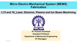
  • 1. 14/09/2023 1 L15 and 16_Laser, Electron, Plasma and Ion Beam Machining Micro Electro-Mechanical System (MEMS) Fabrication Dr. Poonam Sundriyal Assistant Professor Department of Mechanical Engineering IIT Kharagpur
  • 2. 14/09/2023 2 LASER Beam Machining (LBM) Focusing Solar radiation on a paper Intensity of sun at earth’s surface = 1 kW/m2 Focusing Light radiation on workpiece Laser power density = 1.9x10⁷ kW/m2 • Can melt all the materials (including diamond)
  • 3. • Spontaneous absorption • Spontaneous emission • Stimulated emission Laser interaction with an Atom A. Spontaneous absorption B. Spontaneous emission LEL HEL LEL: Lower energy level/ Ground state, HEL: Higher energy level/ Excited state : electron , : energy photons, 14/09/2023 3 Light Amplification by Stimulated Emission of Radiation HEL2 HEL1 C. Stimulated emission parent stimulated
  • 4. 14/09/2023 4 Major Applications ➢ Photolithography ➢ Laser Cutting of Metal Sheets, Paper, Glass, Plastics, Textiles, Rubber, Ceramic, etc. ➢ Laser Micro-welding. ➢ Laser scribing, marking, engraving Applications of Laser in MEMS LaserForming ➢ Laser Surface Cladding ➢ Laser Rapid Manufacturing ➢ Laser polymerization ➢ Laser Metal Forming ➢ Laser Surface Alloying LaserScribing LaserCladding LaserRapidPrototyping
  • 5. 14/09/2023 Characteristics of LASER 1. Lasers are monochromatic: they have single output wavelength or a pure color with an extremely narrow bandwidth. • Depending on the laser type, they can have wavelength from ultraviolet through visible and even in the infrared portion of the electromagnetic spectrum. • Wavelength selection is important dependent on the material being processes. Analysis of objects at a certain energy is important for research purpose. Red (660 & 635 nm), green (532 & 520 nm) and blue-violet (445 & 405 nm) lasers 3. Lasers are highly directional/ low divergence • Lasers have been bounced off the moon to accurately measure the distance between moon and earth. LED 2. Highly coherent: all waves are exactly in phase with one another. Light bulb 5
  • 6. 14/09/2023 6 Laser cutting dominants the industrial laser applications & has more than 75% of share of all LM applications. • Fast cutting with higher quality than other competing processes. Basic Principle : Melting with a focused laser beam and molten material ejection by a high-pressure gas jet. • Excimer Laser, NdYAG & Fiber Lasers • Laser Power = 500-5000W • Focal spot size ~ 0.1 – 0.3 mm • Power density of 1kW power at focal spot of 0.3mm ~ 1.4 X10⁶ W/cm2 • Effect on material * Melting * Vaporization • Pressurized co-axial gas jet ejects the molten / vaporized material Laser Cutting
  • 7. 14/09/2023 7 Energy balance equation: No conduction loss P = w.t.v. (Cp.Tm + Lf + m’Lv) In cutting, m’ =0 Cutting speed, v = P / {w.t. (Cp.Tm + Lf )} P/v.t = w. (Cp.Tm + Lf ) /  = S, Constant for a constant w & a given material Called as “Severance Energy” in (J/mm2) where,  = (1-R) Laser Power Coupling coefficient, R = Reflectivity of job material P = Laser power, t = Sheet thickness, w = cut or kerf width, v = cutting speed, Lf = latent heat of fusion, Lv = latent heat of vaporization, m’=Fraction of metal evaporated,  = density, T = Temperature raise, Cp = Specific Heat, Energy balance in Laser Cutting w t v Energy required for cutting (Ecutting) = Ereaching to melting temperature from ambient temp + Ephase change from solid to liquid + Ephase change from liquid to vapour (mass flow rate (ṁ) = density * area * velocity) Moving laser for cutting
  • 8. 14/09/2023 8 Drilling with Long and Ultra-short Laser Pulses • Longer pulses continuously heat the material during the pulse duration. • Heat conduction: HAZ, recast layer, microcracks. • Ultrashort laser pulses : a few ps or below • Due to the extremely short pulse duration, only electrons are heated at first. • Energy transfer to the lattice takes place on a timescale longer than the pulse itself. - Heat conduction is limited. • This finally leads to ablation within a well-defined region with minimum thermal and mechanical damage to the surrounding
  • 9. 14/09/2023 9 z a Energy balance consideration in Laser Beam Drilling Energy required for drilling (Edrilling) = Ereaching to vaporization temperature from ambient temp + Ephase change from solid to liquid + Ephase change from liquid to vapour (mass = density * volume) Laser position - fixed
  • 10. Characteristics CO2 Laser Nd:YAG Laser Diode Lasers Excimer Lasers Fiber Laser Wavelength m 9.6-10.6 1.06 0.8-1.0 0.193-0.354 1.06 Laser power, CW Pulse energy Upto 45 kW 1-20 J 50W- 2kW 1-100J Up to 4kW --Avg.1kW 1-10J, 10kW Efficiency % 10-15 2–20 20-40 2-3 30 Beam Diverg. 1-3 mr. 1 – 25 mr. 1x200 mr 2 – 6 mr. 1-2 mr. Beam Transportation Reflecting mirrors Optical fibers Optical fibers Optical fibers Optical fibers Absorption in metals Low ~2-15% Moderate ~5-30% Moderate ~5-30% High 50% Moderate ~5-30% Life, CW (Hrs.) Pulsed (Shots) ~ 1000s. ~106 ~200 Life of ~106 lamps ~ 1000s. 104-107 (one gas fill) Size of lasers Large Moderate Compact Moderate Compact Maintenance intervals (Hr) 1000-2000 500-1000 5,000-10,000 500-1000 5,000-10,000 Mode of operation CW & Pulsed: ms- sub-s CW & Pulsed: ms- Sub-ps CW & Modulated Pulsed 10’s ns CW & Pulsed: ms- Sub-ps 14/09/2023 10 Lasers for Material Processing Applications and their Characteristics
  • 11. 14/09/2023 11 Electron Beam Machining (EBM) • Electron beam is used for machining. • Electrons are generated by thermionic emission from hot tungsten cathode. • Thermionic emission : emission of electrons from an electrode due to its temperature. thermal energy provided to the charge carrier > work function of the material (binding potential). Fig. Schematic of thermionic emission process LEL HEL LEL: Lower energy level/ Ground state, HEL: Higher energy level/ Excited state : electron , : energy, -ve +ve
  • 12. 14/09/2023 12 • Spot diameter: 10- 200 µm and Power density = 6500 billion W/mm2 = 6.5 × 10¹⁸ W/mm2 • Any material can rapidly melt and vaporize. • EBM is a very precise vaporization process. • Basic Process: EBM - Thermal process, similar to LBM. (done in vacuum) Material-heating: Striking of high-velocity electrons with workpiece. Kinetic energy of electrons Heat Rapid melting and vaporizing Electron Beam Machining (EBM) • Applications: Mask Fabrication for Photolithography, Imaging, Drilling fine holes, cutting narrow slots, welding, and rapid manufacturing.
  • 13. 14/09/2023 13 Rotating shutter Electron beam gun: Electrons are generated by thermionic emission from hot tungsten cathode. In E-beam gun for cutting & drilling applications, there is a grid between anode & cathode on which negative voltage is applied to pulse / modulate the e-beam. Components of Electron Beam Machining Power supply: Up to 150 kV, Current : 150 µA- 1.5A. Vacuum-chamber: 10-4-10-6 Torr (1 Torr = 1 mm Hg) achieved by rotary pump backed diffusion pump. Vacuum compatible CNC workstation Mode of E-beam Operation: For drilling and cutting - Pulsed electron beam Single pulse : A single hole in thin sheet; Multiple pulses: To drill in a thicker material. For welding : DC electron beam Parameters so chosen that loss of material due to vaporization is minimum.
  • 14. 14/09/2023 14 Mechanism of Electron Beam Machining (EBM) Depth of penetration: δ = 2.6 x10 -17 (V 2 /ρ) mm where, V=Accelerating voltage (Volts) and ρ = Material density (kg/mm3) Figure: Movement of an electron below surface * Unaffected zone: Transparent layer * Energy of Electrons Lattice of material through collisions. * Energy transfer Function of kinetic energy or accelerating voltage. • Maximum rise in temperature- At a certain depth, not at the surface, unlike laser heating. Change in Kinetic Energy of Electron = me(u - uo)2/2 eV, u (km/s) ~ 600√(V) me= 9.1x10⁻³¹kg, e =1.6 x10⁻¹⁹ Coulomb. KE is dissipated in the impinging material. Power requirement for machining: P = CQ where, C = Constant of proportionality or specific power consumption in EBM , and Q = Material removal rate
  • 15. 14/09/2023 15 Q. What will be the penetration depth of the electron beam accelerated at 150 kV impinging in steel having density of 76 × 10-7 kg/mm3? Numerical Solution: δ = 2.6 x10 -17 (V 2 /ρ) mm δ = 77 µm Q. An electron beam of 5 kW power is used for cutting a 150 µm wide slot in 1 mm thick tungsten sheet. Determine the cutting speed? (Specific power consumption in EBM (constant of proportionality) for tungsten is 12 W/mm3/min) Solution: P = CQ Let the speed of cutting be V mm/min. Q = AV = 150 × 10-3 × 1 × V mm3/min P = CTungusten Q 5000 = 12 × 150 × 10-3 × 1 × V V = 2778 mm/min = 4.6 cm/sec
  • 16. Source: Intel Mask Fabrication using Electron Beam Machining
  • 17. 14/09/2023 17 1. Localized heating of work-piece: On an organic or synthetic backing * E-beam focal spot diameter ≤ Desired diameter * Power density : ~108 W/cm2, sufficient to melt & vaporize any material. 2. Vaporization of a small fraction of melted material • Recoil pressure of escaping vapour pushes the molten material aside creating a hole. 3. E-beam penetrates in till it reaches the bottom surface of work piece. 4. Removal of material: As e-beam strikes the auxiliary support volume in contact is totally vaporized resulting in the explosive release of backing material vapour * High velocity vapour carries along with it the molten walls of the capillary, creating a hole in the work piece and a small cavity in the backing material. Electron Beam Drilling Process: Four Stages
  • 18. 14/09/2023 18 Energy Balance in EBM Energy balance considering the kerf will be governed by Thermal Diffusion length ( ddif = 2√(ατ)) as the E-beam spot size is usually smaller than ddif. ηP = w.t.v.ρ.Cp. ∆T w= kerf width ≈ Thermal diffusion length ≈ 2 ατ = 2 α𝑑/𝑣 Where, η =E- beam power coupling efficiency including conduction loss ≈ 0.1, P = E-beam power in W; t= depth of penetration in m up to which rise in temperature is ∆ T, α = Thermal diffusivity = k/ ρ. Cp k= Thermal conductivity of material in W/mºC ρ =Material density in g/m3; Cp = Specific heat in J/kg. ºC; τ = E-beam material interaction time (For continuous e-beam scanned at velocity, v interaction time, τ = d/v ) d= width of e-beam in m; v= Processing speed in m/s
  • 19. 14/09/2023 19 Plasma Arc Manufacturing (PAM) What is Plasma? • This is the 4th state of matter – Ionized gas (Electrically conducting and responsive to magnetism) • Electrically neutral -numbers of negative charge (electron + negative ions) and positive charge equal. Ex: Ionized air (plasma) What is an Arc? • An electric arc is a discharge of electric current across a gap in a circuit. • An arc discharge is characterized by a low voltage and relies on thermionic emission of electrons from the electrodes supporting the arc. -It can be sustained by plasma. Electric arc
  • 20. 14/09/2023 20 Introduced in 1957. Similar to Gas Tungsten Arc Welding (GTAW): Electric Arc is formed between an electrode and work piece. Key difference from GTAW: • In PAW electrode placed in the torch and arc is infused with gas. • Plasma arc separated from shielding gas • Plasma forced through a fine-bore copper nozzle : Constricts the arc and the plasma exits the orifice at high velocities and high temperature ~ 20,000 °C. Plasma transfers the electric arc to the work piece. Metal to be welded is melted by the intense heat of the arc and fuses together. Higher energy concentration : Deeper and narrower welds and Increased welding speed. Plasma Arc Welding (PAW) Fig. Schematic of TIG Fig. Schematic of PAW
  • 21. 14/09/2023 21 Operating Modes in PAW Micro-plasma: 0.1 to 15 A PAW was first developed for low current welding of thin materials (less than 0.1 mm thickness) since TIG could not provide stable arc at low currents. Micro-plasma arc can be operated at very low welding currents. • Widely used in electronics industries to weld thin sheets of all materials. Medium current: 15 to 100 A. Process characteristics of the plasma arc are similar to the TIG arc, however because plasma is constricted, arc is more concentrated, thus is capable to weld faster & better than TIG . • deeper penetration (from higher plasma gas flow), greater tolerance to surface contamination (the electrode is within the body of the torch) and better tolerance to variations in standoff distance. (up to 2.4 mm thickness) • Welding of thin film (foil thickness) materials: Most applications of plasma welding are in the low-current range, from 100 amperes or less.
  • 22. Room Temperature Plasma • Surface cleaning • Surface modification using oxygen, nitrogen, etc. • Surface adhesion improvement – Important for coating and additive processing. • Change of wettability. • Etching https://plasmatreatment.co.uk/knowledge-base/videos
  • 23. 14/09/2023 23 Ion Beam Machining (IBM) - Nanofabrication • A type of particle beam consisting of ionized atoms i.e. ions. Sputtering: • A stream of ions of an inert gas, such as argon or metal such as gallium is accelerated in a vacuum by high energies and directed toward a solid workpiece. • Ion beam knocks off atoms from workpiece by transferring kinetic energy and momentum to atoms on the targeted surface. Fig. Schematic of sputtering process Kinetic Energy> Binding Energy Ion atoms
  • 24. 14/09/2023 24 Why IBM is better for Nanomanufacturing
  • 25. 14/09/2023 25 • In a Liquid metal ion source (LMIS), a metal (typically gallium) is heated to the liquid state and provided at the end of a capillary or a needle. (Tm= 29.8 º C) • An electric field (108 V/cm) is applied to the end of the wetted tip that causes the liquid Ga to form a point source (2-5 nm tip) in the shape of “Taylor cone”. • Conical shape forms because of electrostatic and surface tension force balance. • An extraction voltage (negative) pulls Ga from the tip and efficiently ionizes it by field evaporation of the metal at the end of the Taylor cone. Liquid Metal Ion Source (LMIS) -ve
  • 26. 14/09/2023 26 Most commonly used in Liquid Metal Ion Source because of the following characteristics: 1. Low Ionization Potential of Ga = 6eV 2. Low melting (Tm= 29.8 º C) minimizes any reaction or inter-diffusion between liquid and tungsten needle substrate. 3. Low volatility at melting point conserves the supply of metal and yields a long source life 4. Good viscous property; no drop off 5. Excellent mechanical, electrical and vacuum properties Why Gallium?
  • 27. 14/09/2023 27 • A Vacuum system and chamber • A liquid metal ion source (LMIS) • An ion column for milling and deposition • A precision Goniometer stage for sample mounting and manipulation • Imaging detectors • A gas injection system to spray a precursor gas on the sample surface • An electron column for imaging • Scan generators for ions and electrons • Computer control Components of FIB system Beam energy ~ 30 or 50 keV Beam current ~1 to 20 nA, Best image resolution ~5 -7 nm, and Vacuum Chamber pressure ~ 10 -7 mbar
  • 28. 14/09/2023 28 Sputtering rate as the depth of surface layer sputtered per unit time: V(nm/s) = 0.1 S (M/d) J. Cosθ where, S -sputtering yield (atoms/ion), M -atomic (molecular) weight (g) of target, d -target density (g/cm3), J -ion current density (mA/cm2) and θ -angle of incidence • Only ~5% of ion energy spent for sputtering, 95% is scattering in other processes, mainly heating the target. • However, the power density on the surface of target = 0.6 W/cm2, so the target will be heated less (usually up to 50- 90 ºC). • One of the main advantages of ion beam treatment -we can work with a lot of temperature sensitive materials! Sputtering Yield in IBM • Sputter yield depends on the energy of the incident ions, angle of incidence on the surface of work-piece, masses of ions and target atoms, and the binding energy. Sputter Yield, S = No. atoms removed / No. of striking Ions
  • 29. 14/09/2023 29 Basic Operating Modes in IBM • Emission of secondary ions and electrons FIB Imaging (Low ion current) ✓Sputtering of substrate atoms • FIB Milling (High ion current) ✓Chemical interactions (Gas assisted) • FIB Deposition • Implantation • Enhanced Etching Imaging Milling Deposition Implantation
  • 30. 14/09/2023 30 Focused Ion Beam (FIB) Setup
  • 31. 14/09/2023 31 FIB Milling Typical material removal rate is about 1 m3 per second. • In FIB milling, typically a gallium (Ga) primary ion beam hits the sample surface and sputters away a small amount of material. • If the ion energy is adequate the collision can transfer sufficient energy to the surface atom to overcome its surface binding energy ( 3.8 eV for Au and 4.7 eV for Si). • At high primary currents, material can be efficiently removed from the sample surface, allowing precision milling of the sample with achievable feature sizes of well below 1 µm. • At the same time, the sample can be imaged with very high precision. Note: There are other variants of the process like Reactive Ion Etching (RIE) where chemical species are incorporated, and the process proceeds chemically.
  • 32. 14/09/2023 32 FIB Deposition For FIB induced deposition, the necessary processes are: • Adsorption of the chemical precursor gas onto the sample surface. • Decomposition of gas molecules into volatile and non-volatile products by focused ion beam. 3 dimensional nanostructures can be fabricated using layer by layer deposition. Precursor must have two properties, namely : • Sufficient sticking probability to stick to a surface of interest in sufficient quantity. • Decompose more rapidly than it is sputtered away by the ion beam.
  • 33. 14/09/2023 33 • Etching / Milling of all material, Reactive etching, Substrate cleaning: Subtractive • Deposition: Sputter deposition - Additive • Ion- beam Lithography – Pattern transfer • Ion-beam implantation – Doping Applications of Ion Beam Machining
  • 34. 14/09/2023 34 Applications of Ion Beam Machining STM Tips SAMPLE COURTESY UNIVERSITY ROUEN Coil 700 nm pitch, 80 nm line width, diamond like amorphous carbon, Fabricated by FIB induced deposition 50 nm size holes patterned on a thin film using IBM Deposition and machining using FIB
  • 36. 14/11/2023 1 L17_Biomimetic for MEMS Fabrication Micro Electro-Mechanical System (MEMS) Fabrication Dr. Poonam Sundriyal Assistant Professor Department of Mechanical Engineering IIT Kharagpur
  • 37. Manufacturing of Biomimetic Materials/ Surfaces and Devices https://www.nature.com/arti cles/s41427-021-00322-y
  • 38. 14/11/2023 3 Biomimicry Nagel, Ph. D. Dessertation, 2011 https://www.researchgate.net/publication/45812610_Systematic_design_of_biologically-inspired_engineering_solutions • Meaning: To imitate life. • Design inspired by nature. • Biomimicry Inspired by Nature (1997): Book by Janine Benyus. • Biomimicry is an approach to innovation that seeks sustainable solutions to human challenges by emulating nature’s time- tested patterns and strategies. Antibacterial Surface Self-cleaning Adhesion Heat Transfer Optical
  • 39. Biomimicking: Self cleaning (Hydrophobic) Surfaces • The Lotus Effect: The surface of lotus leaves are bumpy, and this causes water to bead as well as to pick up surface contaminates in the process. • The water rolls off, taking the contaminates with it. • Self cleaning surfaces. • Application in solar cell, fabrics, healthcare. https://link.springer.com/content/pdf/bfm:978-3-7643-8321-3/11/1.pdf https://phys.org/news/2016-06-lotus-leaf-scientists-world-self-cleaning.html
  • 40. Replication Methods: Micro Replication Double Inversion (MRDI) https://doi.org/10.1002/admi.201701052
  • 41. 14/11/2023 7 Structural Color – useful for photonics • Structure design is responsible for color, not pigments – environment friendly and stability. • Light reflection due to structural design. • Diffraction grating and thin-film interference. • Structural color- no fading. • Application: Photonics. • Fabrication methods: Lithography, self- assembly, templating/ MRDI, etc. https://www.sciencedirect.com/science/article/pii/S007964251300025X https://www.sciencedirect.com/science/article/pii/S014372082200941X
  • 42. Replication Methods: Sacrificial Metal 3D Printing – For High Aspect Ratio (AS) Figure. Proposed processing workflow. (a) CAD model of the thin-walled sacrificial metallic mold designed as the “negative” of the desired PDMS structure (in this case, a slender pillar with AR = 50). (b) 3D printing of the metallic mold using LPBF. (c) Drop-casting and curing PDMS inside the metallic mold. (d) Etching the sacrificial mold in an acidic solvent to release the desired PDMS structure. https://pubs.acs.org/doi/full/10.1021/a csami.0c21295
  • 43. Biomimicking: Climbing robot inspired by Lizard /Gecko https://royalsocietypublishing.org/doi/10.1098/rspb.2020.2576 • Nanoscopic hairs. • Strong grip: These millions of tiny, flexible hairs exert van der Waals forces that provide a powerful adhesive effect.
  • 46. 14/11/2023 1 Microfluidics Micro Electro-Mechanical System (MEMS) Fabrication Dr. Poonam Sundriyal Assistant Professor Department of Mechanical Engineering IIT Kharagpur
  • 47. 14/11/2023 2 • Microfluidics is the area of science and technology that is focused on simple or complex, mono‐ or multiphasic flows that are circulating in natural or artificial micro systems with at least, one dimension is in μm. • Inkjet printer in 1950. • Microfluidics in 1990. Microfluidics for MEMS
  • 48. 1. Unique physical and chemical effects, mass and heat transfer characteristics 2. Small volumes of expensive and/or dangerous reagents 3. Parallel operation 4. Portability, integration (reactions, separation, detection) 5. Implanting microfluidic devices in biological systems 6. Compatibility with other micro/nanoscale device Why Microfluidics?
  • 49. 14/11/2023 4 Applications of Microfluidics in MEMS
  • 50.
  • 51. 14/11/2023 6 Basics of fluid mechanics: Scaling Laws • Things start behaving differently as we gradually shrink their sizes. • Forces and quantities of significance: oVolume (L3) becomes less significant. oArea (L2) becomes more important. oLength (L) starts to dominate. Capillary action in different sized diameters Capillary action in nature
  • 52. Basics of fluid mechanics: Non- Newtonian Fluids • Non-linear relationship between shear stress and shear strain. Examples: paint, blood, ketchup, cornstarch solution • Types of fluid flow: oLaminar oTurbulent 14/11/2023 8
  • 53. • Laminar flow: o Fluid particles move along smooth paths in layers o Most of energy losses are due to viscous effects o Viscous forces are the key players and inertial forces are negligible • Turbulent flow: o An unsteady flow where fluid particles move along irregular paths o Inertial forces are the key players and viscous forces are negligible • Reynolds number: Re = inertial force/ viscous force = ρvL/µ o Re < 2000 for laminar oDue to small dimensions o Re < 1 in microfluidic systems Basics of fluid mechanics: Laminar and Turbulent Flow Fig: Flow within Microfluidic Device entering from the right and exiting as one channel. 14/11/2023 9
  • 54.
  • 55. Wettability • Ability of a liquid to maintain contact with a surface • Adhesion (l-s) vs. cohesion (l-l) • Contact angles are a way to measure liquid-surface interactions 14/11/2023 11
  • 56.
  • 57. • Developed by Langmuir (1917), and refined by Blodgett • Used to produce thin polymer films at molecular scale. • It produces more than a single monolayer of various compositions onto a substrate to create a multilayer structure. • The monolayer is formed by spreading the organic molecules on the water sub-phase. MEMS & microsystems Design and manufacture,Tai-Ran Hsu, McGraw Hill http://www.abo.fi/student/en/Content/Document/document/10911 • Amphiphilic long chain molecules usually have hydrophilic (head) and hydrophobic (tail) parts → molecules stand on their heads when film is formed • Very loosely packed on water → gas phase • The surface pressure can be increased by means of one or two sliding barriers. • Analogous to transition from gas → liquid → solid phase. Langmuir–Blodgett (LB) Film
  • 58. Fundamentals of Microfabrication:The Science of Miniaturization, Second Edition By Marc J. Madou LB deposition on hydrophilic surface Formation of mono layer 2nd layer deposition Up to 100 layers LB deposition on hydrophobic surface Formation of Langmuir–Blodgett (LB) Film
  • 59. • Controlled optical properties such as refractive index and anti reflectivity → Ideal materials for micro sensors and optoelectronic devices. • Ferroelectric polymer thin films in sound transducers in air, water, tactile sensors, biomedical applications. • Coating materials with controllable optical properties in broadband optical fibers for transmitting laser light at different wavelengths. • Microsensors – the electric conductivity of the polymer sensing element will change when it is exposed to a specific gas. MEMS & microsystems Design and manufacture,Tai-Ran Hsu, McGraw Hill Applications of Langmuir–Blodgett (LB) Film https://opg.opt ica.org/oe/fullt ext.cfm?uri=oe -24-24- 27184&id=354 671
  • 61. Chemical mechanical polishing (CMP) Ajay Sidpara Mechanical Engineering Department IIT Kharagpur http://www.surfaceprocess.com/ | http://www.siliconwafers.net/
  • 63. Starting point of silicon processing • More than 90% of the earth's crust is composed of Silica (SiO2) or Silicate • Silicon is the principle platform for semiconductor devices • Semiconductor technologies require monocrystalline Si with precise uniform chemical characteristics (controlled dopant and oxygen content). • Transform raw silicon into a useable single-crystal substrate begins by mining for relatively pure Silicon Dioxide. • Most silicon is made by reduction of SiO2 with Carbon in an electric furnace from 1500 to 2000 ͦ C. • With carefully selected pure sand, commercial brown Metallurgical Grade (MG) Silicon of 97% purity or better. • It is further purified to bring impurities below the ppb level. • Eventually it is used for semiconductors by further processing. http://www.cleanroom.byu.edu/EW_formation.phtml Sand MG silicon
  • 64. Basic steps in silicon wafer preparation CMP
  • 65. Czochralski method (CZ) • It is used for fabrication of single crystal silicon by melting of poly crystal silicon with additional dopants as required for the final resistivity. • A single crystal silicon seed is placed on the surface and gradually drawn upwards while simultaneously being rotated. • Impurities (Oxygen and Carbon) • Quartz (SiO2) gradually dissolves, releasing large quantities of oxygen into the melt. • More than 99% of this is lost as SiO gas from the molten surface, but the rest stays in the melt and can dissolve into the single crystal silicon. • The silicon monoxide evaporating from the melt surface interacts with the hot graphite susceptor and forms carbon monoxide that re-enters the melt. http://meroli.web.cern.ch/meroli/Lecture_silicon_floatzone_czochralski.html
  • 66. Float zone silicon (FZ) • A high-purity alternative to CZ process. • A high-purity PC rod and a MC seed crystal that are held face to face in a vertical position and are rotated. • With a RF heating both are partially melted. The seed is brought up from below to make contact with the drop of melt formed at the tip of the poly rod. • As the molten zone is moved along the polysilicon rod, the molten silicon solidifies into a single Crystal and, simultaneously, the material is purified. • Multiple zone refining can be performed on a rod to further reduce the impurity concentrations. • The melt never comes into contact with anything but vacuum (or inert gases), there is no incorporation of impurities that the melt picks up by dissolving the crucible material as in CZ method. • It is not easily used at large diameters. http://meroli.web.cern.ch/meroli/Lecture_silicon_floatzone_czochralski.html
  • 67. Silicon plane identification • Crystals are characterized by a unit cell which repeats in the x, y, z directions. <111> n-type <100> p-type <100> n-type <111> p-type Identifying flats on silicon wafers
  • 68. 8 What is CMP? • CMP of silicon wafers is a basic processing technology for the production of flat, defect free, highly reflective surfaces. • CMP combines the actions of wet chemical etching with mechanical polishing. • The mechanical component removes the wet-etch residues, leading to a highly planar process. • The basic principle: Use a chemical reaction to soften material and then mechanically polish off this layer. http://www.ntu.edu.sg/home/mdlbutler/Research/Research_CMP.htm
  • 69. Chemical – soften film Mechanical – “Polish” off softened film 9 Wafer – pad – slurry interaction at micro/nano scale Micro scale The rough pad carrying the particle-based slurry interacts with the surface of the wafer and participate in mechanical abrasion. Nano scale The kinetics of formation and removal of thin surface layer controls CMP output parameters such as material removal rate, surface planarity rate, and surface defects. Singh and Bajaj, Advances in Chemical–Mechanical Planarization, MRS BULLETIN/OCTOBER 2002
  • 70. Device architectures scaled down to sub micron scale Increasing number of layers 10 Si substrate Lithography: Resolution ~ Depth of Focus CMP Si substrate New planarization technique Local : R=2 -100 and 30o> θ> 0.5o Global : R>> 100 and θ< 0.5o Why use CMP? Surface planarization Local planarization: Smoothing techniques that increase planarity over short distances. Global planarization: Techniques that decrease long-range variations in wafer surface topology (entire wafer)
  • 71. tabl e Slurry (chemical+abrasive) Conditioner Head Platen Wafer Pad 11 Typical Process Conditions  Pressure: 10 to 50 kPa  Platen/Carrier rpm: 10 to 100 rpm  Velocity: 10 -100 cm/s  Slurry flow rate: 50 to 500 ml/min  Typical removal rates:  Oxide CMP ~2800Å/min  Metal CMP ~3500Å/min Typical parameters setting
  • 72. 12 Single and multiple wafer carrier
  • 73. 13 Difference between chemical etching and CMP Singh and Bajaj, Advances in Chemical–Mechanical Planarization, MRS BULLETIN/OCTOBER 2002 CMP Chemical etching Both process achieve controlled material removal. But mechanisms are different. • Material removal is by chemical reaction at the surface  formation of dissolved species  subsequent transportation of the dissolved species from the surface. • Etching rate does not change with time. • The reactions between the chemicals and the metallic layers result in a thin, non-dissolving, chemically passivating surface film  it is subsequently removed by the mechanical action of the abrasive particles. • Initially, the chemical reaction rate is high, but due to passivation effects, the reaction rate drops immediately. • Surface-film formation and passivation phenomena repeat.
  • 74. 14 Mechanical polishing • Direct interaction between abrasive particles. • Indentation of surface and material removal by scratching process. • Requires high energy to break bonds using mechanical forces. • MRR much lower than CMP. • Large abrasive particles  high MRR but resulting surface defects. • Inverse relationship between MRR and surface finish. Removal rate and surface finish obtained using chemical etching, mechanical polishing, and CMP Removal rate and surface finish obtained using chemical etching, mechanical polishing, and CMP Lapping CMP Difference between mechanical polishing and CMP Singh and Bajaj, Advances in Chemical–Mechanical Planarization, MRS BULLETIN/OCTOBER 2002 CMP  Chemically modified surface layer is much more easily removed because of its inherent nature.  A soft, ductile layer in the case of silica and more brittle layer in the case of metals such as tungsten and copper.
  • 75. 15  Slurry: Abrasive particles, chemicals such as oxidizers, surfactants, polymer additives, pH stabilizers, salts, and dispersants;  Particle size, shape, concentration, dispersion, pH, chemical additives, and chemical concentration. Interactions  Chemical–surface interactions  resulting in surface modification of the wafer.  Particle–wafer interaction  leading to shear and normal stresses, indentation and material removal,  Particle-particle interaction  Fluid-flow-surface interaction  chemical corrosion and etching, mechanical polishing, and pad modification and degradation. CMP Process parameters
  • 76. 16 Effect of process parameters • Polish time  Amount of material removed and Planarity • Pressure on wafer carrier (down force)  Removal rate, Planarization and non-uniformity • Platen speed  Removal rate and Non-uniformity • Carrier speed  Material selectivity and Removal rate • Slurry flow rate  Affects how much slurry is on the pad and the lubrication properties of the system • Pad conditioning  Removal rate, Non-uniformity, and Stability of CMP process • Wafer/slurry temperature  Removal rate • Wafer back pressure  Wafer breakage
  • 77. Polishing pad http://s3-alliance.com, http://www.gohanmi.com, http://www.eminess.com, http://www.nanofinishcorp.com,
  • 78. • It executes the polishing action, and transmits the normal and shear forces required for polishing. • Cost adding element, dominating effect on CMP process • It is a porous, flexible polymer material made up of a matrix of cast polyurethane foam with filler material to control hardness of polyurethane impregnated felts • Filler improve mechanical properties • Polyurethanes have a unique property of high strength, high hardness and modulus combined with high elongation at failure. • Pad materials: durable, reproducible, compressible Polishing pad Zantye et al., Chemical mechanical planarization for microelectronics applications, Materials Science and Engineering R 45 (2004)
  • 79. • Polishing pad surface roughness determines the conformality range. – Smoother pad  poorer topographical selectivity  less planarization effect. – Rougher pad  longer conformality range  better planarization polishing result – Hard pad does not approach to step cavities – Soft pad can reach to most of the cavities • WIWNU : with-in wafer non-uniformity • WTWNU : wafer to wafer non-uniformity Polishing pad: surface roughness and hardness Soft Pad Hard Pad http://www.me.ntut.edu.tw/introduction/teacher/lu/IC%20fabrication_GA/IC_%20Chp%2012.pdf.
  • 80. • Conditioner is a stainless steel plate coated with nickel-plated diamond grits. • Pad becomes smooth due to the polishing • Need to recreate rough pad surface • In-situ pad conditioner for each pad • Use – It resurfaces the pad – Removes the used slurry – Supplies the surface with fresh slurry Polishing pad conditioner http://www.me.ntut.edu.tw/introduction/teacher/lu/IC%20fabrication_GA/IC_%20Chp%2012.pdf.
  • 81. Four classes of pads : 1. Class I (trade name as PellonTM, SubaTM), felts and polymer impregnated felts Types of polishing pad http://cmplab.re.kr/board/pds/board_download.php?file=pds0134_1.ppt&dn=1 • Continuous channels between fibers • Slurry loading capacity: Medium • Typical applications: Si stock polish, Tungsten CMP Top view Cross section
  • 82. Four classes of pads : 2. Class II (trade name as PolitexTM , SurfinTM , UR100TM ), microporous synthetic leathers; Types of polishing pad http://cmplab.re.kr/board/pds/board_download.php?file=pds0134_1.ppt&dn=1 • Vertically oriented open pores • Slurry loading capacity: High • Typical applications: Si final polish, Tungsten CMP, Post CMP buff Top view Cross section
  • 83. Four classes of pads : 3. Class III (trade name as IC1000TM , IC1400TM), filled polymer films Types of polishing pad http://cmplab.re.kr/board/pds/board_download.php?file=pds0134_1.ppt&dn=1 • Closed cell foam • Slurry loading capacity: Low • Typical applications: Si stock, inter layer dielectric (ILD) CMP, shallow trench isolation (STI) metal damascene CMP Top view Cross section
  • 84. Four classes of pads : 4. Class IV (trade name as OXP 3000TM, IC1400TM), unfilled textured polymer films with major structural characteristic as felted fiber with polymer binder Types of polishing pad http://cmplab.re.kr/board/pds/board_download.php?file=pds0134_1.ppt&dn=1 • Non-porous polymer sheet with surface macro texture • Slurry loading capacity: Minimal • Typical applications: ILD CMP, STI CMP, metal dual damascene Cross section
  • 85. Comparison of polishing pads http://cmplab.re.kr/board/pds/board_download.php?file=pds0134_1.ppt&dn=1 Type 4 Type 3 Type 2 Type 1 Non-porous polymer sheet with surface macrotexture Microporous polymer sheet Porous film coated on a supporting substrate Felted fibers impregnated with polymeric binder Structure None Closed cell foam Vertically oriented, open pores Continuous channels between fibers Microstructure Minimal Low High Medium Slurry loading capacity OXP3000TM, IC2000TM IC1000TM, IC1010TM, IC1400TM, FX9TM, MHTM PolitexTM, SurfinTM, UR100TM, WWP300TM PellonTM, SubaTM Pad examples Very Low Low High Medium Compressibility Very High High Low Medium Stiffness Very High High Low Medium Hardness ILD CMP, STI, Metal dual damascene Si stock, ILD CMP, STI, Metal damascene CMP Si final polish, Tungsten CMP, post-CMP buff Si stock polish, Tungsten CMP Typical applications
  • 86. • Pad Hardness – controlled during polymerization –quantified by Young’s Modulus o 2 GPa – hard pad – good global planarity o 0.5 GPa – medium pad – good local planarity o 0.1 GPa– soft pad – smoothing • Pad Asperities o Pore diameter : 30~50 µm o Peak to Peak : 200~300µm Types of polishing pad Zantye et al., Chemical mechanical planarization for microelectronics applications, Materials Science and Engineering R 45 (2004)
  • 87. • Subjected to elevated temperature due to frictional forces at solid–solid contact • Local heating of the pad leads to rise in temperature up to 30oC. • The effects of pad heating are compounded if the chemical reaction between slurry and pad is exothermic. • Mechanical, physical and chemical properties of the polyurethane material permanently or temporarily altered if heated beyond limit. • Local pad temperature during CMP may increase significantly, especially at the localized points of contacts between pad and wafer. • To avoid additional pressure, the pad is operated in the temperature range within which its co-efficient of thermal expansion is to zero. Effect of temperature on polishing pad Zantye et al., Chemical mechanical planarization for microelectronics applications, Materials Science and Engineering R 45 (2004)
  • 88. 28 How to achieve global planarization? The process parameters must be optimized such a way that • Minimize mechanical removal of the material (to reduce frictional forces and avoid the damage to surface topography) • Low frictional forces ►MRR compromised ► more processing time. • Variation in local polishing pressure ► variable removal rates within the wafer • Excessive chemical etching ► affects surface planarity and induces defects on the surface such as corrosion Zantye et al., Chemical mechanical planarization for microelectronics applications, Materials Science and Engineering R 45 (2004) Steigerwald et al., Chemical Mechanical Planarization of Microelectronic Materials, Wiley and Sons, New York (1997). • The key to a good polishing step  Synergy between chemical etching and mechanical planarization with minimization of both the phenomena. Un-planarized (completely conformal) Surface smoothing Local planarization Global planarization
  • 89. Important parameters of slurry: pH, concentration and size of abrasives, complexing agents, oxidizers, buffering agents, surfactants, corrosion inhibitors, etc. An ideal CMP slurry should be able to achieve  high removal rate,  good surface finish,  excellent global planarization,  should prevent corrosion (in case of metal CMP, especially Cu),  high selectivity. • Contributing factors for high MRR – Surface reaction – The time scale at which the passivation layer is formed 29 CMP slurry Zantye et al., Chemical mechanical planarization for microelectronics applications, Materials Science and Engineering R 45 (2004)
  • 90. To reduce the defect level, • the machining unit (abrasive particle size) must be minimized. • Nano-sized abrasives • increased shear stress. • Additional chemical energy 30 How to reduce defect? www.cmplab.re.kr/board/pds/board_download.php?file=pds0090_1.pdf&dn=1
  • 91. • If the pH is reduced below 7 or if salt is added  the units tend to fuse together in chains. These products are often called "silica gels”. • If the pH is kept slightly on the alkaline side  the subunits stay separated. These products are often called “silica sols”. 31 Colloidal Silica Synthesis http://qdfsk.en.alibaba.com/product/1083971851-214441075/basic_colloidal_silica_ludox_silica_sol.html http://www.media.pearson.com.au/schools/cw/au_sch_chandler_qs1_1/int/solutions.html
  • 92. 32 Agglomeration of CMP Slurry • The ideal slurry has abrasives crystallized as discrete single particles. • Aggregates  assembly of multiple particles with strong physical or chemical attachment • Agglomerates  particles and/or aggregates that come together into close-packed clumps that are not sufficiently ionically charged to provide permanent suspension • Cause micro scratches due to deep indentation or non-uniformity due to differential polishing pressure. • How to avoid agglomeration?  Milling at the point of slurry manufacture, filtration and proper electrolyte balance. Zantye et al., Chemical mechanical planarization for microelectronics applications, Materials Science and Engineering R 45 (2004) http://www.semiconductoronline.com/doc/techniques-for-evaluating-particles-in-cmp-sl-0001 Silica Agglomerates and Large Particles
  • 93. • Too small flow rate  friction force increases, temperature non-uniform and reduces the flatness of polished silicon wafer. • Material will not be removed uniformly at the pad-film contact point • Large flow rate  resultants rapidly separate from silicon surface, reduce. • Silicon polishing is exothermic  Temperature is increased at the interface. – Change in reaction kinetics of the slurry with the wafer, mostly increasing the removal rate. • Too high temperature  polishing slurry easy to volatilize, chemical reaction is too rapid  leading polishing haze. • Increase in temperature  viscoeleastic polyurethane pad softer  reduce removal rate due to the reduction in hardness. • Temperature is optimized to 20–30º C. 33 Slurry flow rate
  • 94. • Size, concentration, hardness • Material removal depends on material removed by single abrasive particles and total number of active abrasive particles. • As particle size and hardness increases the MRR increases. • Increase in particle concentration  increase the number of active particles  more number of indentations to the passivating film  high MRR. • Increase in particle size or hardness  rise to surface defects such as micro-scratches that cause fatal long-term device failure. • Bigger and harder particles  deeper micro-scratches, which will be very difficult to eliminate even by the final buffing CMP step. • Optimum level of particle concentration for high MRR. 34 Abrasive particles
  • 95.   p dz K P V dt    dt dz : Material Removal Rate 35 Preston’s Equation for CMP P : Pressure p K : Preston coefficient V : Velocity • Simplest and most widely used equation • It can predict the general trend • Kp depends on surface chemistry, abrasion effects & part-polisher contact. Weaknesses • Good enough for mechanical polishing. Does not account for any chemical synergistic effects. • Fails to provide any insight into the interaction process (e.g., the effects of particle size, concentration, and other slurry and pad variables). • Cannot predict WIWNU, feature effects, or variations due to pattern density effects
  • 96. Need to modify the Preston’s Eq. 36 Need to develop new fundamental mechanistic approach considering synergistic mechanical and chemical effects, and nonlinearities due to pad-wafer interaction. Preston’s Equation • The material removal rate is usually over-estimated • originally proposed for glass polishing (hard pad) • the coefficient KP is responsible for all unknown effects • a threshold pressure often exists • the definition of V is vague   p dz K P V dt     
  • 97. 37 Particle less slurry for copper CMP • Slurry handling a bit difficult in CMP. • Improper handling and mixing of slurry particles result in agglomeration. • Abrasive free slurry developed to overcome teething defects • The abrasive free slurry employs chemicals to soften the oxide layer (i.e. Cu-complex) on Cu (softer than oxide of Cu in conventional slurry), polishing pad removes Cu-complex
  • 98. Chemical reactions and abrasive particles introduce surface defects and contaminations.  Surface defects mainly consist of mechanical abrasion leading to damaged layer, mechanical inclusions of particles on the surface, chemical effects, etc.  Corrosion effects: Corrosion inhibitors eliminate free metal ions from the solution and prevents redeposition of metal residue.  In Cu polishing benzotriazole (BTA) is used as a corrosion inhibitors.  Particles contamination Based on the various surface forces like van der Waals forces and electrostatic forces, particles get adhered onto the surface. Physically embedded onto the surface due to the pressure applied by the polishing pad.  Metallic contamination observed mainly in metal CMP process as adsorbed ions, oxides, hydroxides and salts. 38 Defects and contamination
  • 99. 39 Surface Particle Embedded Particle Rip out Residual Slurry Micro- scratch Dishing Ref.: Philipossian et al. (2001) CMP Defects
  • 100. Brush scrubbing mechanism • Particles are removed from wafers by mechanical force provided by the brush bristles. • Brushes are made of polyvinyl alcohol (PVA) material, the texture of which is soft when wet. • Uses hydrodynamic drag to exert a removal force on the surface particles. 40 Post CMP cleaning process Limitation • Cost of ownership. • Cannot clean a batch of wafers at one time, • limitation of life of the brush • In case of smaller particles (less than 1μm) or physically embedded particles hydrodynamic drag is not enough  needs brush-particle contact for complete particle removal.
  • 101. Chemical wet cleaning • It has the advantage of low cost of ownership and high throughput as several wafers can be cleaned simultaneously in batches. • It gives lower efficiency when compared to the scrubber mechanism. Hydrodynamic jet cleaning • Impinging pressure jets on the wafer surface. • Low pressure jets: to avoid wafer surface damage and more effective for small particles. • Pressure to remove micron (big) size particles is more than sufficient to damage patterned surfaces. Spin-rinse drying • Particles and chemicals on the surface are removed by centrifugal force along with the application of low-pressure sprays. Ultrasonic and megasonic cleaning • This involves introducing pressure waves in a cleaning bath using acoustic transducers. 41 Post CMP cleaning process
  • 102. 42 Si CMP Si SiO2 Oxide CMP and metal CMP Oxide CMP • Alkaline solution with silica • pH at 10 to 12 by additives Metal CMP • Acidic solution with alumina • pH at 2 to 6 After CMP Blanket Metalization Cu Patterning Dielectric SiO2 Barrier Layer Deposition Ta CMP
  • 103. 43 Other applications of CMP https://www.crystec.com/alpovere.htm • To planarize oxide, poly silicon or metal layers in order to prepare them for the following lithographic step, avoiding depth focus problems, etc. • The Si substrate gets a Si3N4 layer on top of it.  patterned and etched. • The shallow trenches are then filled with oxide. • CMP step  to remove all oxide from the top of the Si3N4 layer. • Transistor can be built by gate oxide and poly-silicon gate formation. • SiO2 is deposited thicker than the final thickness requested. • Step heights removal  to get a good flat surface for the next level. (ILD)
  • 104. 44 Other applications of CMP https://www.crystec.com/alpovere.htm • Metals like W, Al or Cu are used in damascene process technology to fill vias or trenches in order to prepare electrical connections. • A planarized dielectric surface is patterned with vertical contact holes. • Tungsten (W) is deposited using CVD. • CMP step  to remove the surface tungsten, leaving behind the filled contact holes. • Highly selective in removing the tungsten versus the underlying dielectric. • Finally a metal layer is patterned on top of the filled contacts to complete the circuit.
  • 105. Remarks Advantages Achieves global planarization and wide range of wafer surfaces can be planarized Planarization Useful for planarizing multiple materials during the same polish step. Planarize multi material surfaces Provides an alternate means of patterning metal (e.g., Damascene process), eliminates the need of plasma etching for difficult-to-etch metals and alloys. Alternative method of metal patterning Contributes to increasing IC reliability, speed and yield (lower defect density) of sub-micron devices and circuits. Increased IC reliability CMP is a subtractive process and can remove surface defects. Reduce defects Does not use hazardous gases common in dry etch process. No hazardous gases 45 Advantages of CMP
  • 106. 46 Remarks Disadvantages There is relatively poor control over the process variables with a narrow process latitude. Poor control of process parameters New types of defects from CMP can affect process yield. These defects become more critical for sub-micron feature sizes. New defects CMP requires additional process development for process control and metrology. Ex. the endpoint of CMP is difficult to control for a desired thickness. Need for additional process development CMP is expensive to operate because of costly equipment and consumables. CMP process materials require high maintenance and frequent replacement of chemicals & parts. Cost of ownership is high Disadvantages of CMP
  • 107. 47
  • 108. Doping and Surface micromachining (deposition) Ajay Sidpara Mechanical Engineering Department IIT Kharagpur
  • 109. Energy requirements for various physical processes Fundamentals of Microfabrication:The Science of Miniaturization, Second Edition By Marc J. Madou Incoming particles Reaction Ion energy (eV) either reflected or physisorbed Physical adsorption < 3 • Kinetic energy of the incoming particles largely dictates which events are most likely take place at the bombarded surface. Surface migration and surface damage Some surface sputtering 4 – 10 Substrate heating, surface damage, material ejection (sputtering or ion etching) Sputtering 10 – 5000 Ion implantation (doping) Implantation 10k – 20k
  • 110. Doping of silicon Introduction to Microfabrication, 2nd Edition Sami Franssila • Introduction of suitable n- or p-type dopants into the silicon. • It is used to change the electrical properties of semiconductors. • Dopants can be introduced into silicon by five different methods: – during crystal growth – by neutron transmutation doping (NTD) – during epitaxy – by diffusion – by ion implantation • The first two techniques are applied to whole ingots, and epitaxy results in a uniformly doped layer all over the wafer.
  • 111. Doping of silicon by diffusion Introduction to Microfabrication, 2nd Edition Sami Franssila • Diffusion is the movement of atoms along concentration gradients. – Atoms from high-concentration areas move to areas of lower concentration. • It is a technique to introduce and drive boron, phosphorus and other dopant atoms into the silicon lattice. • Thermal diffusion is a high-temperature process: Range of 900–1200 °C • Batch process  long process times are compensated by a huge loads, 100 or even 200 wafers, in a batch. • It can be done from the gas phase. • In gas phase doping the wafers are put in a furnace and a suitable doping gas, POCl3 for phosphorus doping, or BBr3 for boron doping, is introduced. • The wafers are exposed to dopant atom vapors and doped.
  • 112. Doping of silicon by thin film diffusion Introduction to Microfabrication, 2nd Edition Sami Franssila • The alternative technique is diffusion from doped thin films. • For example, boron-doped polysilicon, phosphorus-doped silica glass (PSG) or doped spin-on glass is deposited on the wafer, which is then put into a furnace. • Dopants from the doped film diffuse into the silicon. • The junction depth (xj) is the depth where diffused dopant concentration equals substrate dopant concentration.
  • 113. Diffusion mechanism Introduction to Microfabrication, 2nd Edition Sami Franssila • Dopant atoms move with the help of point defects: they jump to vacancies and interstitials. • Interstitial diffusion: Atoms jump from one interstitial site to another interstitial site. Diffusion for small atoms (sodium and lithium). • Substitutional/vacancy: Diffusion necessitates that an empty lattice site is available next to the diffusing atom. – At high temperatures substitutional sites are thermally created. Antimony and arsenic demonstrate substitutional mechanisms. • Interstitialcy: It is related to the substitutional mechanism: self- interstitial atoms move to lattice sites, and knock dopants out to interstitial sites, and from there they move to lattice sites. • Boron and phosphorous are expected to diffuse via interstitialcy mechanism.
  • 114. Mathematical modelling by Fick’s law MEMS & microsystems Design and manufacture,Tai-Ran Hsu, McGraw Hill • For C1 > C2 • Expression may be written in a different form of equation: Ca = (dopant flux) Concentration of A at a distance x away from the initial contacting surface /m2-s Xo = position of the initial interface of A and B. Ca,xo, Ca,x = respective concentrations of A at xo and x. D = (diffusion coefficient) diffusivity of A into B - a material constant for specific pair of materials in the process. • D usually increases with temperature → higher efficiency at elevated temperature Concentration (C1) of a liquid A in liquid B with distinct concentration (C2) is proportional to the difference of the concentrations of the two liquids but is inversely proportional to the distance over which the diffusion effects takes place.
  • 115. Time dependent diffusion MEMS & microsystems Design and manufacture,Tai-Ran Hsu, McGraw Hill • Duration of diffusion (time) plays an important role in the variation of the concentration of liquid A. • Substrates are heated to a carefully selected temperature and then dopant is made available at the surface of the substrate. • Masking is necessary to dope selectively and controlled manner. • The dopant can diffuse into the substrate until a maximum concentration is reached. This maximum concentration of dopant through diffusion is called solid solubility.
  • 116. Ion implantation • Ion: electrically charged atoms or molecules. • -ve ion  an atom contains more electrons than that in its neutral state. • +ve ion  an atom contains fewer electrons than it is necessary to maintain the neutral state. • Ionization: process of producing ions. • 2 methods for production of discrete ions and ion beams – Electrolysis process – By electron beams • Extreme energy is required to initiate and maintain the ionization process. • Ionization energy: the energy needed to remove the outermost electron from an atom of the ionized medium. • 2nd ionization energy is higher than the 1st Ionization energy and so on. MEMS & microsystems Design and manufacture,Tai-Ran Hsu, McGraw Hill
  • 117. Ionization by electron beam • Ions are extracted from the certain substances gaseous state (plasma) by electron beams. • Electrons are generated by heating the cathode in a electron gun. • Then they are guided by a set of electrodes to an accelerator. • Accelerator  high voltage electric field supplies the necessary kinetic energy to accelerate the flow of passing electrons. • Electron beam containing high kinetic energy collides with the molecules of the medium in the ionization chamber. • It results in ionizing the medium after knocking out electrons from the medium atoms. MEMS & microsystems Design and manufacture,Tai-Ran Hsu, McGraw Hill • H and He gases are popular ion sources. • BF3 for extracting +ve B ion.
  • 118. Ion implantation • It is physical process used to dope silicon substrates. • “Forcing” free charge-carrying ionized atoms of B, P or As into silicon crystals. • These ions carry sufficiently high kinetic energy to penetration into the substrate. • Ion beam is led into a beam controller (adjustment of size and direction of beam) • Accelerator: a tube for energizing ions in the beam to attain the final energy with which the ions will impact the substrate surface. • Mask for controlling the area of doping. MEMS & microsystems Design and manufacture,Tai-Ran Hsu, McGraw Hill • Ions enter the substrate  collide with electrons of the substrate  transfer all their energy to the substrate after collision  come to stop at a certain depth.
  • 119. Ion implantation process Introduction to Microfabrication, 2nd Edition Sami Franssila • Ions penetrate into silicon and into the mask, too. • The mask has to be thick enough so that it will block ions. • Photoresist, oxide, nitride and poly-silicon are typically used as mask materials. • The higher the implantation energy, the deeper the ions will penetrate, and the lighter the ion, the deeper it will go. • Straggle ΔR is the deviation in range, the width of the depth distribution. (a) Implantation: mask layer blocks selected areas; (b) dopant concentration profile inside silicon, with projected range RP and straggle ΔR Concepts for implanted ions: R: range is the length of ion travel; RP is the projected range, and RL lateral straggle
  • 120. Masking in ion implantation Introduction to Microfabrication, 2nd Edition Sami Franssila • Photoresist can mask ion implantation, an obvious advantage over thermal diffusion which requires an oxide mask. • Masking layers for ion implantation have to be substantially thicker than projected ranges, to ensure that the ions do not penetrate the mask. • Photoresist masking it is easy to spin-coat thick enough resists to block ions. • Stripping of implanted resist difficult due to – Accelerated ions break bonds due to their high energy. • This can lead to resist carbonization, especially if high doses are used. – Wafers also heat up during implantation because accelerated ions carry a lot of energy. • This heating will further bake the resist and change its structure.
  • 121. Advantages and disadvantages of ion implantation Introduction to Microfabrication, 2nd Edition Sami Franssila • Implantation today is the main method of introducing dopants into silicon, and it has almost replaced thermal diffusion. Advantages: • Able to place any ion at various depths in the sample • Independent of the thermodynamics of diffusion and problems with solid solubility and precipitation. • Does not require high Temp. (little thermal stress or strain) Disadvantages: • Dopant distribution is not uniform. • Ion beams produce crystal damage which reduces electrical conductivity. – This damage can be eliminated by annealing at 700 to 1000 °C.
  • 123. Surface micromachining • It builds microstructures by deposition and etching of different structural layers on top of the substrate. • Polysilicon is commonly used as one of the layers and SiO2 is used as a sacrificial layer. (Layers thickness varying from 2-5 μm). • Advantages: – Possibility of realizing monolithic microsystems  electronic and mechanical components (functions) are built in on the same substrate. – Substrate's properties are not as important  structures are built on top of the substrate and not inside it  expensive silicon wafers can be replaced by cheaper substrates, such as glass or plastic. – The size of the substrates can also be much larger than a silicon wafer.
  • 124. Thin film deposition techniques • Chemical Vapor Deposition (CVD) – Reactant gases introduced in the chamber, chemical reactions occur on wafer surface leading to the deposition of a solid film. – Earlier used in IC industry for Si and dielectric deposition due to good quality films and good step coverage but now extended to metals also. – e.g. APCVD, LPCVD, PECVD. • Physical Vapor Deposition (PVD) (no chemical reaction involved) – Vapors of constituent materials created inside the chamber, and condensation occurs on surface leading to the deposition of a solid film. – Mainly used for metal deposition which is difficult by CVD. – E.g. evaporation, sputter deposition, etc. • Other methods that are gaining importance in ULSI fabrication: – Coating with a liquid that becomes solid upon heating, e.g. spin-on-glass used for planarization. – Electro-deposition: coating from a solution that contains ions of the species to be coated. E.g. Cu electroplating for global interconnects. – Thermal oxidation. Prof. Bo Cui, ECE, University of Waterloo; http://ece.uwaterloo.ca/~bcui/
  • 125. Thin film application in MEMS • Thin films provide dielectric functions (e.g. capacitors, interlayer insulation), encapsulation (e.g. moisture barriers), sacrificial layers, and anti-stiction surfaces in MEMS devices. • Use of thin films to create membranes with desired characteristics for RF switches, microphones, opto-acoustic modulators and cantilevers. • Flammable gas detectors in the chemical industry where the heating and sensing elements are mounted on top of a silicon nitride diaphragm. (www.plasmatherm.com - Silicon Nitride for MEMS Applications: LPCVD and PECVD Process Comparison Microphone (electronicdesign.com) MEMS RF switch (www.intechopen.com) Cantilever as a sensing element (nanolithography.spiedigitallibrary.org) surface acoustic wave platform using various sensing thin films deposited on the piezoelectric resonant line (http://www.tms.org/pubs/jou rnals/JOM/0010/Ivanov/Ivan ov-0010.html )
  • 126. Typical steps in thin film deposition 1. Introduce reactive gases to the chamber. 2. Activate gases (decomposition) by heat or plasma. 3. Gas absorption by substrate surface . 4. Reaction take place on substrate surface, film formed. 5. Transport of volatile byproducts away from substrate. 6. Exhaust waste. Prof. Bo Cui, ECE, University of Waterloo; http://ece.uwaterloo.ca/~bcui/
  • 128. Chemical vapour deposition • CVD is the most important process in microfabrication. • Used for producing thin films over the surface of silicon substrates, or over other thin films already been deposited to the silicon substrate. • Materials for CVD may include: – Metals: Al, Ag, Au, W, Cu, Pt, etc. – Organic materials: Al2O3, poly Si, SiO2, Si3N4, piezoelectric ZnO, SMA TiNi, etc. • There are 3 available CVD processes in microfabrication: – APCVD (Atmospheric-pressure CVD) - Elevated temperature but at near atmospheric pressures (105 Pa) – LPCVD (Low-pressure CVD) - Utilizes vacuum (< 10 Pa) to increase deposition rate and uniformity – PECVD (Plasma-enhanced CVD) - Enhancing the reactions and permitting very low deposition temperatures • CVD usually takes place at elevated temperatures and in high class clean rooms. MEMS & microsystems Design and manufacture,Tai-Ran Hsu, McGraw Hill
  • 129. CVD sources and substrates • Types of sources – Gasses – Volatile liquids – Sublimable solids – Combination • Source materials should be – Stable at room temperature – Sufficiently volatile – High enough partial pressure to get good growth rates – Reaction temperature < melting point of substrate – Produce desired element on substrate with easily removable by-products – Low toxicity • Substrates – Need to consider adsorption and surface reactions – For example, WF6 deposits on Si but not on SiO2 Prof. Bo Cui, ECE, University of Waterloo; http://ece.uwaterloo.ca/~bcui/
  • 130. Working principle of CVD • CVD involves the flow of a gas containing diffused reactants (normally in vapor form with an inert carrier gas) over the hot substrate surface. • The gas that carries the reactants is called “carrier gas”. • The carrier gas and the reactant flow over the hot substrate surface  surface temperature provokes chemical reactions of the reactants  formation of films during and after the reactions. • The “diffused” reactants are foreign material that need to be deposited on the substrate surface. • The by-products of the chemical reactions are then let to the vent. MEMS & microsystems Design and manufacture,Tai-Ran Hsu / Introduction to Microfabrication, 2nd Edition Sami Franssila H2 Ar H2+PH3 H2+B2H6 HCl SiCl 4 H2 Silicon wafers Graphite susceptor Quartz reaction chamber RF induction (heating) coils vent SiCl 4 + 2H2  Si + 4HCl
  • 131. CVD reactions • Homogeneous reactions occur before the gas molecules reach the surface. – reaction rate at the surface is reduced due to consumption of the gas reactants before reaching the substrate. – The result is a low-density and normally, a poorer quality film. • Heterogeneous reactions occur on or near the substrate surface and as the reactant gasses reach the heated substrate. – produce good quality films because of the proximity of the reaction to the wafer’s surface. • Heterogeneous reactions are preferred over homogeneous reactions. Southwest Center for Microsystems Education (SCME) www.scme-nm.org • Reaction rate affects the deposition rate and quality of the deposited layer. • Both phases are greatly affected by temperature. High temp  high reaction rate.
  • 132. Control of CVD Introduction to Microfabrication, 2nd Edition Sami Franssila CVD processes depend on both chemical reactions and flow dynamics. There are two main cases: • Surface reaction limited (high supply but less reaction/consumption) • High flow rate supplies enough reactants and film deposition is limited by slow surface chemical reactions. • Arrival rate of reactants is less important. • Mass transport limited or diffusion limited (high reaction/consumption but less supply) • Fast surface reaction consumes source gas rapidly and the deposition rate is limited by gas supply. • Reaction rate cannot proceed any faster than the rate a which the reactant gases are supplied to the substrate by mass transport. • Temperature is less important.
  • 133. Film growth rate in CVD J. Plummer, et al.,-Silicon VLSI Technology - Funds, Practice and Mdlg-Prentice-Hall (2000) • F1 = diffusion flux of reactant species to the wafer through the boundary layer = mass transfer flux • F2 = flux of reactant consumed by the surface reaction = surface reaction flux, where hG is the mass transfer coefficient (in cm/sec). Cg and Cs is concentration of species on the top of the boundary layer and at the substrate surface (molecules/vol.) where kS is the surface reaction rate (in cm/sec). In steady state: F = F1 = F2 • The growth rate of the film (cm/s) is now given by where N is the number of atoms per unit volume in the film (cm-3) or density of the film
  • 134. Film growth rate in CVD J. Plummer, et al.,-Silicon VLSI Technology - Funds, Practice and Mdlg-Prentice-Hall (2000) • Y = CG / CT Incorporating species is Si, CG is the number of molecules of SiCl4 per cm3 in gas phase, CT is the total number of SICL4 and H2 molecules ( plus any other species) per cm3 in the gas phase • Now, growth rate of the film (cm/s) is given by where Y is the mole fraction (partial pressure/total pressure) of the incorporating species and CT is the concentration of all molecules in the gas phase. where PG is the partial pressure of SiCl4 and Ptotal is the total pressure in the system • Y is also defined as PG / Ptotal For Example
  • 135. Example of Film growth rate in CVD J. Plummer, et al.,-Silicon VLSI Technology - Funds, Practice and Mdlg-Prentice-Hall (2000) • hG = 1 cm/sec • ks = 10 cm/sec • Partial pressure of incorporating species = PG = 1 torr • Total pressure = Ptotal = 760 torr • Total concentration of gas phase = CT = 1019 cm-3 • Density of depositing film = N = 5 x 1022 cm-3 v is in cm/sec while film thickness is generally measure in µm/min
  • 136. Film growth rate in CVD J. Plummer, et al.,-Silicon VLSI Technology - Funds, Practice and Mdlg-Prentice-Hall (2000) (a) If kS << hG,  surface reaction controlled case: (b) If hG << kS,  mass transfer controlled case: • ks increases with temperature. (Arrhenius with Ea depending on the particular reaction, e.g. 1.6 eV for single crystal silicon deposition). • hG ≈ constant (diffusion through boundary layer is insensitive to temperature) kS is the surface reaction rate (in cm/sec). hG is the mass transfer coefficient
  • 137. Compensation for boundary layer and depletion effect • Position of the boundary layer as a function of x J. Plummer, et al.,-Silicon VLSI Technology - Funds, Practice and Mdlg-Prentice-Hall (2000) • δs increases along the length hG decreases • Deposition rate decreases from the front of the susceptor to the back. • Source gas depletion occurs  concentrations decrease with distance. • Solution  Tilted wafer susceptor • decreases the cross sectional area along the length of the chamber. • gas velocity to increase  boundary layer to decrease  increases the growth rate downstream. hG = mass transfer coefficient, DG = Diffusivity of reacting gas, δS = boundary layer thickness • Impose a 5-25° temperature gradient along the tube length
  • 138. Reactors of CVD Prof. Bo Cui, ECE, University of Waterloo; http://ece.uwaterloo.ca/~bcui/ • kS (surface reaction) limited deposition is VERY temperature sensitive. • hG (mass transfer) limited deposition is VERY geometry (boundary layer) sensitive. • Si epitaxial deposition is often done at high T to get high quality single crystal growth. • hG (mass transfer) controlled, and horizontal reactor configuration is needed for uniform film thickness across the wafer. • When a high film quality is less critical (e.g. SiO2 for inter-connect dielectric), deposition is done in reaction rate controlled regime (lower temperature). • Throughput can be greatly increased the by stacking wafers vertically.
  • 139. Reactors of CVD MEMS & microsystems Design and manufacture,Tai-Ran Hsu, McGraw Hill Horizontal reactor Vertical reactor • Various types of CVD reactors are built to perform the CVD processes. Horizontal reactor: • Resistance heaters are placed around the chamber. Vertical reactor: • Resistance heaters are placed under the susceptor that holds the substrate.
  • 140. Problems with APCVD • Wafer throughput is low due to low deposition rate. • Film thickness uniformity can be an issue. • Step coverage is not very good. • Contamination is a problem. • Large number of pinhole defects can occur. • Problem – If operated at high T, a horizontal configuration must be used (few wafers at a time). – If operated at low T, the deposition rate goes down and throughput is again low. • The solution is to operate at low pressure. http://www.timedomaincvd.com/CVD_Fundamentals/Fundamentals_of_CVD.html
  • 141. Low Pressure Chemical Vapor Deposition (LPCVD) • Diffusion through boundary layer Plummer et al., Silicon VLSI Technology Prof. Bo Cui, ECE, University of Waterloo; http://ece.uwaterloo.ca/~bcui/ hG = mass transfer coefficient DG = Diffusivity of reacting gas δS = boundary layer thickness P = pressure where • So as Ptotal goes down, DG and hence hG will go up. – when pressure reduced from 760 Torr (1 atmosphere ) to 1 Torr (760x), hG increases by ~100x (because δS increases by only 3-10x).  Is always < tube radius. /760, U,  • Higher hG means higher T can be used while still ks < hG (i.e. still in surface reaction controlled regime). • Velocity of mass transport will decrease  substrates can approach more closely and the deposited films show better uniformity and homogeneity.
  • 142. Low Pressure Chemical Vapor Deposition (LPCVD) • LPCVD reactors: P = 0.2 – 2 Torr, (1 torr = 1/760 atm) T = 500 – 900°C. • Requires no / less carrier gas, and low gas pressure reduces gas-phase reaction ( No contaminants the wafer and system due to particle cluster). • Operates in reaction limited regime  very sensitive to temperature  closely control is required (within +/- 1oC). • 5-25 °C temperature gradient is often created to offset source gas depletion effects and use distributed feeding. • Transport of reactants from gas phase to surface through boundary layer is still not mass transfer rate limiting (despite the high T)  wafers can be stacked vertically for high throughput (100-200 wafers per run). • Deposits simultaneously on front and back of wafer. • Used to deposit SiO2, Si3N4, Polysilicon (few nm to many µm) Prof. Bo Cui, ECE, University of Waterloo; http://ece.uwaterloo.ca/~bcui/
  • 143. Working of LPCVD • Quartz tube placed in a spiral heater at very low pressure around 0.1 Pa. • The tube is heated to the desired temperature • Wafer surface temperatures typically in the 600°C to 800°C range. • Gaseous species is inserted into the tube at 10-1000 Pa pressure. – It consists of dilution gas and the reactive gas that will react with the substrate. • The working gas spreads out around the hot substrates  reacts with the substrates  forms the solid phase material  the excess material is pumped out of the tube. • The primary reaction mechanism is thermal decomposition on the wafer. G. Logan Liu, Department of Electrical and Computer Engineering, University of Illinois Urbana-Champaign
  • 144. A Laboratory LPCVD Machine G. Logan Liu, Department of Electrical and Computer Engineering, University of Illinois Urbana-Champaign
  • 145. Advantages of LPCVD • Lowering the total pressure of the gas stream increases the diffusion and extends the reaction controlled regime to higher temperature. • It enables close packed stacking (vertical loading) of wafers in LPCVD chambers  high throughput • Lower chemical reaction temperature • Due to lower pressures, there are fewer defects. – Less gas phase reaction  fewer particulates form that can deposit on the wafer. • No / less need of carrier gas (not transport limited)  less dependence on gas flow dynamics http://www.timedomaincvd.com/CVD_Fundamentals/Fundamentals_of_CVD.html
  • 146. Disadvantages of LPCVD • Virtually no gas phase collisions occurs in the near-surface region  line- of-sight transport as opposed to more randomly directed diffusional transport (as in APCVD) – Shadowing occurs  affects step coverage and filling. • Operating temperature that requires cycling from room temperature to as high as 800°C. – Temperature cycling may generate stress on fragile device features that can cause irreversible structural damages. • Reaction precursor is consumed preferentially from start to end  the furnace temperature must be spatially ramped (~ 50 - 70°C) to ensure equal deposition rate. – film stress for wafers at one end of the batch may differ from wafers further away from the reactant injection point. • Surface area in the reaction chamber LPCVD needs careful management. – the number of wafers per run must be keep constant – For small and partial batches, “filler or dummy” wafers are used to fill up empty slots. (www.plasmatherm.com - Silicon Nitride for MEMS Applications: LPCVD and PECVD Process Comparison
  • 147. PECVD • Lower temperature processing regime is more suitable for temperature sensitive MEMS devices using magnetic based materials. – Ex.  depositing Si or SiO2 film when Al is already present. Al melting point 660 °C. So, any subsequent processing should be done < 450 °C. • If APCVD or LPCVD is used  deposition rate will be quite low (ks decreases exponentially with T), film quality will be poor (porous and susceptible to moisture absorption). • Plasma (excited by RF or DC) added with reactive gases in the vicinity of the substrate (Thermal + plasma source) (www.plasmatherm.com - Silicon Nitride for MEMS Applications: LPCVD and PECVD Comparison J. Plummer, et al.,-Silicon VLSI Technology - Funds, Practice and Mdlg-Prentice-Hall (2000) • RF-induced plasma transfers energy into the reactant gases, forming radicals that is very reactive. (RF: typically 13.56MHz for PECVD) • High deposition rate at low T • Surface reaction limited deposition  substrate temperature control is important.
  • 148. PECVD Machine G. Logan Liu, Department of Electrical and Computer Engineering, University of Illinois Urbana-Champaign
  • 149. PECVD • Plasma is sustained when high-energy e- strike and ionize atoms and molecules. www.scme-nm.org, Plummer et al., Silicon VLSI Technology, http://www.batnet.com/enigmatics/semiconductor_processing/CVD_Fundamentals/plasmas/plasma_deposition.html Reactant gases High energy e- Ionized in Ionized in to various species Dissociation Ionized and excited molecules (or atoms) Neutral molecules Neutral and ionized fragments of broken- up molecules Free radicals • Free radicals are having incomplete bonding (unpaired electrons). – Ex.  SiO, SiH3 (important for plasma deposition) and F (for plasma etching) • These species are extremely reactive. • They interact and chemically recombine to form a film. • In addition, ion and electron bombardment from the plasma onto the wafer surface can occur.
  • 150. PECVD • Compared to sputtering, pressure is higher (50 mtorr – 5 torr)  ions have less energy when they hit the substrate (more collisions to lose energy)  reduces the sputtering effects on the substrate. • At low T, surface diffusion is slow  high kinetic energy is required for surface diffusion  plasma (ion bombardment) provides that energy and momentum on the reactant gas and atoms and enhances step coverage. Southwest Center for Microsystems Education (SCME) www.scme-nm.org Plummer et al., Silicon VLSI Technology http://www.batnet.com/enigmatics/semiconductor_processing/CVD_Fundamentals/plasmas/plasma_deposition.html
  • 151. Process parameters of PECVD Substrate temperature (100 - 300oC, up to 1000 oC PECVD available) Gas flow (10s to 100s ccm – standard cubic centimeter per minute) • Higher flow rates can increase deposition rate and uniformity Pressure (P  50mTorr – 5Torr ) • Changes the energy of ions reaching electrodes • Can change deposition rate • Increases pressure may lead to chemical reactions in the gas Power (10s to 100s watts) • Affects the number of electrons available for activation and the energy of those electrons • Increased power increases deposition rate but it may lead to chemical reactions in gas Prof. Bo Cui, ECE, University of Waterloo; http://ece.uwaterloo.ca/~bcui/
  • 152. LPCVD vs. PECVD • The fundamental difference between the two technologies is that LPCVD relies upon thermally driven reactions using dichlorosilane (SiH2Cl2), while PECVD uses plasma with SiH4 to lower activation energies required for film formation. • In a direct comparison, LPCVD is perceived as the high-volume, low- cost process and PECVD as the low-temperature alternative. • LPCVD capable of processing over 100 wafers per run at 600 °C to 800 °C versus PECVD, which is typically a single wafer or relatively small batch operating between 200 °C to 400 °C. • PECVD is primarily used for films or wafers that contain layers of film that cannot withstand the high temperatures of the LPCVD systems (www.plasmatherm.com - Silicon Nitride for MEMS Applications: LPCVD and PECVD Process Comparison
  • 153. Advantages of PECVD • Encourage deposition at much lower temperatures and pressures than it would be required for thermal CVD. • Higher film density – Plasma are subject to bombardment by energetic ions (K.E. - few eV to 100's eV. Ion bombardment  dense films and film stress to become more compressive • Chamber easy to clean – Thick films built up on the parts of a chamber may create particles which can fall onto the substrates and cause defects in circuit patterns in semiconductor – By introducing a fluorine-containing gas (e.g. CF4) and igniting a plasma can clean silicon, silicon nitride, or silicon dioxide from the electrodes and chamber. • Good step coverage http://www.timedomaincvd.com/CVD_Fundamentals/Fundamentals_of_CVD.html
  • 154. Disadvantages of PECVD • Film density and stress may also vary depending on the condition of the deposition (plasma bombardment). • Not pure film (incorporation of H2, O2 or N2 is common) – Result in outgassing, peeling, or cracking of the film during subsequent processing . • PECVD systems require wafers to lie flat on the bottom wafer. Only one wafer side can be coated at a time unlike LPCVD (wafers loaded vertically). • Not easy to model the process – Numerous and complicated reactions • Equipment is expensive http://www.timedomaincvd.com/CVD_Fundamentals/Fundamentals_of_CVD.html
  • 156. Physical vapour deposition Introduction to Microfabrication, 2nd Edition Sami Franssila PhysicalVapor Deposition (PVD) http://www.sigmaaldrich.com • Applications: fabrication of microelectronic devices, interconnects, battery and fuel cell electrodes, diffusion barriers, optical and conductive coatings, surface modifications. • PVD is a set of processes used to deposit thin layers of almost any material, typically in the range of few nm to several µm. • It consists of three fundamental steps. 1. Vaporization of the material from a solid source assisted by high temperature vacuum or gaseous plasma. Or knock off or sputter the atoms from a source (target). 2. Transportation of the vapor (or knock-off atoms) in vacuum or partial vacuum to the substrate surface. 3. Condensation onto the substrate to generate thin films.
  • 157. Physical vapour deposition PhysicalVapor Deposition (PVD) http://www.sigmaaldrich.com • Different PVD technologies utilize the same three fundamental steps but differ in the methods used to generate and deposit material. • Atoms can be ejected from the target by • The two most common PVD processes • Thermal evaporation and sputtering – Thermal evaporation relies on vaporization of source material by heating the material using appropriate methods in vacuum. – Sputtering is a plasma-assisted technique that creates a vapor from the source target through bombardment with accelerated gaseous ions (typically Argon). • In both evaporation and sputtering, the resulting vapor phase is subsequently deposited onto the desired substrate through a condensation mechanism. Resistive heating electron beam heating ion bombardment laser ablation
  • 158. Thermal evaporation https://www.mems-exchange.org/MEMS/processes/deposition.html / http://hivatec.ca/consulting-design/thin-film-deposition/ • Substrate is placed inside a vacuum chamber along with a block (source) of the material to be deposited. • The source material is heated to boiling point and evaporate. (deposition rate ~ 0.1 – 1 nm/s) • Vacuum  To allow the molecules to evaporate freely in the chamber, and subsequently condense on all surfaces. • Ultra high vacuum (10-11 Torr)  to avoid collision of atoms. • Method used to the heat (evaporate) the source material 1. E-beam evaporation and 2. Resistive evaporation
  • 159. Resistive evaporation https://www.mems-exchange.org/MEMS/processes/deposition.html / Plummer et al., SiliconVLSITechnology • In resistive evaporation, a tungsten boat (crucible), containing the source material, is heated electrically by tungsten filament with a high current to make the material evaporate. Problems: • As sodium and potassium are used for tungsten filament production. – Contaminants are found in Aluminum evaporation system. • High temperature is limited by filament material. • Contaminants from the crucible as whole material gets melted.
  • 160. E-beam evaporation • More popular than resistance heating. • High energy electron beam is focused at the source material using magnetic field  local heating and evaporation. • A magnetic field is applied to bend the electron trajectory, allowing the electron gun to be positioned below the evaporation line. • Emitted electrons are accelerated by a high voltage potential (kV). • Wide range of materials can be evaporated due to high temperature achieved by e-beam. • Problem: https://www.mems-exchange.org/MEMS/processes/deposition.html / Plummer et al., SiliconVLSITechnology • X-rays can be emitted when e-beam strikes Al. X-ray creates trapped charges in gate oxide. • Annealing of the film is required to remove this damage.
  • 161. How to get better uniformity? • Decrease sample size • Increase distance to substrate – need bigger chamber – need better vacuum – wastes evaporant • Use multiple sources • Move substrate during deposition Very low pressure in PVD, very few gas-phase collision occur  Surface reactions occur very rapidly and very little rearrangement of atoms usually occurs at the wafer surface. Important issues Thickness uniformity Shadowing of surface topography Step coverage https://www.mems-exchange.org/MEMS/processes/deposition.html / Plummer et al., SiliconVLSITechnology
  • 162. Advantages and disadvantages of evaporation Advantages: • Little damage caused to the wafer, since the wafers are not subjected to energetic particles. • Deposited films are usually very pure because the deposition is done in a high vacuum, there are no residual gases or particles to get incorporated in the film. Disadvantages (results in rarely use in mainstream silicon fabrication) • Metals with low vapor pressures, such as W, and films of alloys or compounds with precisely controlled composition are difficult to evaporate. • No in-situ pre-cleaning method available as there is for sputter deposition. • Step coverage and shadow effect. – Very low chamber pressure  mean free path of the gaseous species very large  evaporated deposition species travel essentially in straight lines from the source to the wafer surfaces + limited range of angles Plummer et al., SiliconVLSITechnology
  • 163. Sputter deposition Introduction to Microfabrication, 2nd Edition Sami Franssila • Positive ions (Ar+) from a glow discharge plasma are accelerated by potentials (100s to 1000s eV) and strike the negative electrode with sufficient force to dislodge and eject atoms from the target. • The ejected target atoms will be transported to the substrate wafers in a vacuum. • These atoms are energetic and hit the substrate with considerable energy, which has both beneficial and detrimental effects on the growing film. • Typical sputtering rates are 1–10 nm/s, significantly higher than in evaporation. • Conductive materials can be deposited using a DC sputtering. • Nonconductive films are deposited by using RF sputtering to prevent charging of the target.
  • 164. Sputtering process flow Southwest Center for Microsystems Education (SCME) www.scme-nm.org • The substrate is placed in a chamber with the source material (target) • The chamber is evacuated to the desired process pressure (1–100 mtorr) • An inert gas (such as argon) is introduced. • A plasma is generated using a RF power source  causes the gas to ionize. • +ve ions in the plasma are accelerated to the –ve biased target (few 100 to few 1000 volts –ve related to the plasma). • High-energy ions bombard the target  atoms to break-off as a vapor • Atoms are free to travel through the plasma as a vapor and strike the wafer surface  condense  form the film. • The condensation forms a thin film of source material on all surface (including the substrate).
  • 165. DC Sputtering http://www.uccs.edu/~tchriste/courses/PHYS549/549lectures/sputtertech.html • Sputtering can be achieved by applying large (~2000) DC voltage to the target (cathode). • A plasma discharge will be established and the Ar+ ions will be attracted to and impact the target sputtering off target atoms. • In DC sputtering the target must be electrically conductive otherwise the target surface will charge up with the collection of Ar+ ions and repel other argon ions, halting the process. • Al, W, Ti and other metals can be sputtered.
  • 166. RF Sputter Deposition Plummer et al., SiliconVLSITechnology / http://www.uccs.edu/~tchriste/courses/PHYS549/549lectures/sputtertech.html • Radio Frequency (RF) sputtering will allow the sputtering of targets that are electrical insulators (SiO2, etc). • In DC systems, positive charge builds up on the cathode (target) need 1012 volts to sputter insulators • The target attracts Ar ions during one half of the cycle and electrons during the other half cycle. – Avoid charge build up by alternating potential • The electrons are more mobile and build up a negative charge called self bias that aids in attracting the Argon ions which does the sputtering. • Sputter deposition occurs when target is negative.
  • 167. RF Sputter Deposition Plummer et al., SiliconVLSITechnology / http://www.uccs.edu/~tchriste/courses/PHYS549/549lectures/sputtertech.html • Substrate and chamber make a very large electrode  not much sputtering of substrate. • When frequencies less than about 50 kHz – electrons and ions in plasma are mobile – both follow the switching of the anode and cathode – basically DC sputtering of both surfaces • When frequencies above about 50 kHz – ions (heavy) can no longer follow the switching – electrons can neutralize positive charge build up
  • 168. Magnetron sputtering http://alyssahale.com/design.htm http://www.angstromsciences.com/magnetron-sputtering-deposition http://www.uccs.edu/~tchriste/courses/PHYS549/549lectures/sputtertech.html • Efficiency of ionization in DC and RF is low  only a small % of electrons take part in ionization with Ar atoms low deposition rate. • Magnets are used to increase the % of electrons that take part in ionization. • Magnets are placed below the target material for trapping the electrons near the target and cause them to move in spiral motion until they collide with an Ar atom. • This increases ionization of Ar high sputtering rate  high deposition rate (up to 1 µm/min, 10 to 100 time faster)
  • 169. Magnetron sputtering • Dense plasma is confined to near the target and the ion loss to the wafers is less  unintentional wafer heating is also significantly reduced. • As the ionization efficiency is so large  lower Ar pressure can be utilized (0.5 mTorr). – Less Ar incorporation in the film  better film quality. http://alyssahale.com/design.htm http://www.angstromsciences.com/magnetron-sputtering-deposition http://www.uccs.edu/~tchriste/courses/PHYS549/549lectures/sputtertech.html
  • 170. Evaporation vs. Sputtering http://www.uccs.edu/~tchriste/courses/PHYS549/549lectures/sputtertech.html Limited materials Almost all the materials Little or no control over alloy composition Very tight control over alloy composition
  • 171. Comparison between PVD and CVD • PVD and PECVD are particularly suitable in situations where low process temperature is required. • Safety issue  PVD is better than CVD • Precursors and some by-products are toxic, pyrophoric, or corrosive. • cause issues with material handling and storage. • LPCVD and PECVD are chemical processes  show excellent conformity (edge coating). Choice of process depends on • Type of material to be deposited • Deposition rate • Limitation imposed by the substrate (temperature, size and shape) • Thickness distribution (uniform thickness over non-uniform surface) • Cost • Toxic waste
  • 172.
  • 173. Bulk micromachinng (etching) Ajay Sidpara Mechanical Engineering Department IIT Kharagpur
  • 174. Bulk micromachining • A fabrication technique of mechanical elements by starting with a silicon wafer, and then etching away unwanted parts, and being left with useful mechanical devices. • Typically, the wafer is photo patterned along with protective layer. • The wafer is then submersed into a liquid etchant (e.g. KOH) or dry etchant for etching away any exposed silicon. • Relatively simple, less complex and inexpensive fabrication technology. • Today, almost all pressure sensors are built with Bulk Micromachining. – Bulk Micromachined pressure sensors offer several advantages over traditional pressure sensors. http://www.memx.com/technology.htm / http://www.etchform.com
  • 175. Criteria for Selecting Materials and Etching Solutions Selectivity • Etch rate on structural layer/etch rate on sacrificial layer must be high. Etch rate • Rapid etching rate to reduce etching time Deposition temperature • In certain applications, the overall processing temperature should be low (e.g. integration with CMOS, integration with biological materials) Intrinsic stress of structural layer • To remain flat after release, the structural layer must have low stress Surface smoothness • Important for optical applications Long term stability G. Logan Liu, Department of Electrical and Computer Engineering, University of Illinois Urbana-Champaign
  • 176. Methods of bulk micromachining • There are two main types of methods for Bulk Micromachining: • Dry Etching (solid + gaseous etchant  volatile products) – Gas and Plasma Etching – Reactive Ion Etching – Deep Reactive Ion Etching • Wet Etching (solid + liquid etchant  soluble products) • Etching profile  Anisotropic & Isotropic Basic steps: 1. Transport of etchants to surface (flow and diffusion) 2. Surface processes (adsorption, reaction, desorption) 3. Removal of product species (diffusion and flow). Introduction to Microfabrication, 2nd Edition Sami Franssila || http://home.comcast.net/~dwdm2/MEMS_micromachining.html
  • 177. Selective etching issue Introduction to Microfabrication, 2nd Edition Sami Franssila • All materials can be etched by energetic ions (resist mask and the underlying film, too). • It is important to achieve selectivity (high etch rate ratio between two materials). • In the ideal case  etching would stop when film clears. • But in practice  some underlying material loss is almost inevitable • Resist is also consumed and the sidewall of etched structure is not necessarily perfectly vertical. • Need to decide which degree of profile control and selectivity are acceptable. – once the pattern has been transferred into solid material by etching, rework is much more difficult, and usually impossible. Substrate Underlying material Film Resist
  • 178. Under cutting: Good or bad? Introduction to Microfabrication, 2nd Edition Sami Franssila / http://www.analog.com / http://www.sensorsmag.com • Etching front proceeds as a spherical wave from all points open to the etchant.  Under cutting • Undercut compensation  making the initial mask feature – larger than the desired width (for light-field structures) and – smaller for dark-field structures. • Compensation works quite well for isolated structures, but limited use in dense arrays. Applications • Free standing beam or plates (structure is released when the underlying material is completely removed. • Fabrication of fine and vertical structures (accelerometer)