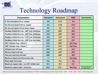
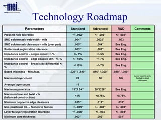
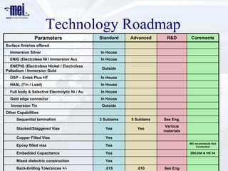
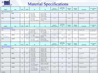
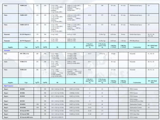
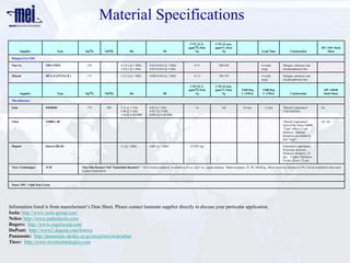
This document outlines the technology roadmap parameters for standard, advanced, and R&D printed circuit board fabrication capabilities including line widths and spacings, via sizes, impedance control tolerances, layer counts, board thicknesses, finishes, and material specifications. Key parameters include line widths down to 2/2.5 microns for advanced technology, microvia sizes down to 0.004 inches, up to 50 layer counts, board thicknesses from 0.016 to 0.3 inches, surface finishes of ENIG, OSP and HASL, and high frequency laminate materials with glass transition temperatures up to 185C and dielectric constants around 4.