An Adaptive Zero Voltage Mechanism for Boost Converter
linesense
1. Controlling the line under-voltage and over-voltage using a
simple resistor network in the Line pin of TOPSwitch-GX
-Srivatsa Raghunath
Under-voltage and over-voltage conditions of the line vary tremendously in India. We
can have an under-voltage of as low as 110V in the urban areas (even less in rural parts)
and the voltage may shoot as high as 310V. Hence, the major challenge for a power
supply designer these days is to ensure steady operation of the power supply under such
wide input conditions and also the dynamic performance must not be affected by it. The
following article shows a simple, but effective way to tackle the above problem using the
most popular device from Power Integrations Inc., the TOPSwitch-GX series.
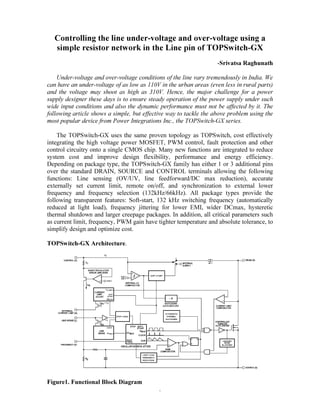
The TOPSwitch-GX uses the same proven topology as TOPSwitch, cost effectively
integrating the high voltage power MOSFET, PWM control, fault protection and other
control circuitry onto a single CMOS chip. Many new functions are integrated to reduce
system cost and improve design flexibility, performance and energy efficiency.
Depending on package type, the TOPSwitch-GX family has either 1 or 3 additional pins
over the standard DRAIN, SOURCE and CONTROL terminals allowing the following
functions: Line sensing (OV/UV, line feedforward/DC max reduction), accurate
externally set current limit, remote on/off, and synchronization to external lower
frequency and frequency selection (132kHz/66kHz). All package types provide the
following transparent features: Soft-start, 132 kHz switching frequency (automatically
reduced at light load), frequency jittering for lower EMI, wider DCmax, hysteretic
thermal shutdown and larger creepage packages. In addition, all critical parameters such
as current limit, frequency, PWM gain have tighter temperature and absolute tolerance, to
simplify design and optimize cost.
TOPSwitch-GX Architecture.
Figure1. Functional Block Diagram
.
2. The LINE-SENSE (L) pin is usually used for line sensing by connecting a resistor
from this pin to the rectified DC high voltage bus to implement line overvoltage (OV),
under-voltage (UV) and line feed forward with DCmax reduction. In this mode, the value
of the resistor determines the OV/UV thresholds and the DCmax is reduced linearly
starting from a line voltage above the under-voltage threshold. The pin can also be used
as a remote ON/OFF and a synchronization input.
Functional Description:
Line Under-Voltage Detection (UV) is explained as follows. At power up, UV keeps
TOPSwitch-GX off until the input line voltage reaches the under voltage threshold. At
power down, UV prevents auto-restart attempts after the output goes out of regulation.
This eliminates power down glitches caused by the slow discharge of larges input storage
capacitor present in applications such as standby supplies. A single resistor (1/2 watt) or
a resistor (1/4 watt) network connected from the Line-Sense pin (Y, R or F package) or
Multi-Function pin (P or G package) to the rectified DC high voltage bus sets UV
threshold during power up. Once the power supply is successfully turned on, the UV
threshold is lowered to 40% of the initial UV threshold to allow extended input voltage
operating range (UV low threshold). If the UV low threshold is reached during operation
without the power supply losing regulation the device will turn off and stay off until UV
(high threshold) has been reached again. If the power supply loses regulation before
reaching the UV low threshold, the device will enter auto-restart. At the end of each auto-
restart cycle, the UV comparator is enabled. If the UV high threshold is not exceeded the
MOSFET will be disabled during the next cycle. The UV feature can be disabled
independent of OV feature.
Line Overvoltage Shutdown (OV) can be achieved from the same resistor used for
UV. Once the voltage exceeds the threshold set by the resistor, TOPSwitch-GX will be
forced into the off-state. The ratio of OV and UV thresholds is preset at 4.5. When the
MOSFET is off, the rectified DC high voltage surge capability is increased to the voltage
rating of the MOSFET (700V), due to the absence of the reflected voltage and leakage
spikes on the drain. A small amount of hysteresis is provided on the OV threshold to
prevent noise triggering. The OV feature can be disabled independent of the UV feature.
Line Feed Forward with DCmax reduction is also achieved from the same resistor
used for UV and OV. This minimizes output line ripple and reduces power supply output
sensitivity to line transients. This line feed forward operation is illustrated in Figure2.
Here for the same control pin current, higher line voltage results in smaller duty cycle
operation. As an added feature, the maximum duty cycle DCmax is also reduced from
78% (typical) at a voltage slightly higher than the UV threshold to 30% (typical) at the
OV threshold. This is illustrated in figure3. Limiting DCmax at higher line voltages helps
prevent transformer saturation due to large load transients in forward converter
applications. DCmax of 38% at the OV threshold was chosen to ensure that the power
capability of the TOPSwitch-GX is not restricted by this feature under normal operation.
3. Figure 2. Relationship of Duty Cycle and Frequency to Control Pin Current.
Figure 3. LINE_SENSE Pin Characteristics
4. Using the LINE-SENSE Pin:
When current is fed into the LINE-SENSE pin, it works as a voltage source of
approximately 2.6V up to a maximum current of 400uA (typical). At +400uA, this pin
turns into a constant current sink. Refer figure4. In addition, a comparator with a
threshold of 1V is connected at the pin and is used to detect when the pin is shorted to the
SOURCE pin.
Figure 4. LINE-SENSE Pin Input Simplified Schematic.
There are a total of four functions available through the use the LINE-SENSE pin:
OV, UV, line feed forward with DCmax reduction, and remote ON/OFF. Connecting the
LINE-SENSE pin to the SOURCE pin disables all four functions. The LINE-SENSE pin
is typically used for line sensing by connecting a resistor from this pin to the rectified DC
high voltage bus to implement OV, UV and DCmax reduction with line voltage. In this
mode, the value of the resistor determines the line OV/UV thresholds, and the DCmax is
reduced linearly with rectified DC high voltage starting from just above the UV
threshold. The pin can also be used as a remote on/off and a synchronization input.
From figure 3 a description of specific functions in terms of LINE-SENSE pin I/V
characteristics can be obtained. The horizontal axis represents LINE-SENSE pin current
with positive polarity indicating currents flowing into the pin. For those that control the
on/off states of the output such as UV, OV and remote ON/OFF, the vertical axis
represents the enable/disable states of the output. UV triggers at Iuv (+50uA typical with
30uA hysteresis) and OV triggers at Iov (+225uA typical with 8uA hysteresis). Between
the UV and OV thresholds, the output is enabled. For line feed forward with DCmax
reduction, the vertical axis represents the magnitude of DCmax. Line feed forward with
DCmax reduction lowers maximum duty cycle from 78% at IL (+60uA typical) to 38% at
Iov (+225uA).
Example: If the UV and OV are specified as 65VAC and 285VAC respectively. Then the
value of the sense resistor is Rl = 92 / (50uA) = 1.8M ohm for UV sense.
R1=404 / (225uA) =1.8M ohm for OV sense.
5. Typical Uses of the LINE-SENSE (L) Pin.
The different configurations in using the L pin is shown below.
.
Figure 5: Line Sensing for Under-Voltage, Overvoltage and Line Feed Forward.
Figure 6: Line-Sensing for Under-Voltage Only (Overvoltage disabled).
Figure 7: Line-Sensing for Overvoltage Only (Undervoltage disabled).
6. Application specified usage of the LINE-SENSE pin.
In the above configurations, the ratio of the OV to UV is fixed at 4.5 throughout;
which means that if the OV cut-off is at 450VDC, then the UV cut-off will take place at
100VDC. This ratio can be altered using the below configuration.
+
-
PT1
G
U1
TOPSwitch-GX
DS
X
C
L
F
R3
4.7k
R1
1.5M
R2
3.3M
D1
36V,1W
Figure 8: Application specified use of line pin (ratio of OV/UV changed).
The calculations are
Vuv / (R1+R2) = 50uA. (1)
(Vov – Vz) / R2 = 225uA. (2)
Example:
If it is required to have an under-voltage (UV) cutoff at 170 VAC and over-voltage
(OV) cutoff at 270 VAC, then the circuit parameters are chosen as follows,
Selecting a 36V ¼ W zener as D1, we get R1+R2 = 4.8M from equation (1) and R2 =
1.5M from equation (2). Thus giving R1=3.3M. Hence, the ratio is now altered to 1.6
from the original value of 4.5.
Also it may be required to have an UV of 100VAC and OV of 300 VAC. Here by
choosing the values of Zener, R1 and R2 as 13V ¼ W, 1M and 1.8M it can be achieved
successfully, reducing the ratio of OV/UV to 3 from the original 4.5.
Application Example:
A typical implementation of a single output AC-DC converter using TOPSwitch-GX
in a Flyback configuration is shown in figure 9. This circuit is designed for 85 V to 265 V
AC input range and 12V, 2.5A output.
Input EMI Filtering
Capacitor CX1 and the leakage inductance of L1 filter differential mode conducted
EMI. Inductor L1 and CY1 filter common mode conducted EMI.
7. Figure 9: 30W, 12V Universal Power Supply.
TOPSwitch Primary
Rectifier Bridge BR1 and C1 provide a high voltage DC supply rail for the primary
circuitry. The DC rail is applied to the primary winding of T1. The other side of the
transformer primary is driven by the integrated MOSFET in U1. Diode D1 and VR1
clamp leakage spikes generated when the MOSFET in U1 switches off. Capacitor C2
reduces the operating temperature of VR1 by bypassing the leading edge of the primary
leakage spike away from VR1. Resistor R3 provides damping to reduce drain ringing
improving EMI. Resistor R1 sets the low-line turn-on threshold to approximately 69
VAC and sets the overvoltage shutdown level to approximately 320 VAC. Resistor R4
sets the U1 current limit to approximately 70% of its nominal value. Resistor R2 reduces
the U1 current limit as a function of line voltage so that maximum overload power is
relatively constant (<50 W) over the entire input voltage range. This limits the output
power delivered during fault conditions. Capacitor C4 bypasses the U1 CONTROL pin
while C3 has three functions. It provides the energy required by U1 during startup, sets
the auto-restart frequency during fault conditions, and also acts to roll off the gain of U1
as a function of frequency. Resistor R5 adds a zero to the control loop to stabilize the
power supply. Diode D2 and capacitor C5 provide rectified and filtered bias power for
U2 and U1.
Output Rectification
The secondary of T1 is rectified and filtered by D3, C6, and C7. Inductor L2 and C8
provide additional high frequency filtering. Resistor R11 and C11 provide snubbing for
D3. Choosing the proper snubber values is important for low zero-load power
consumption and for high frequency EMI suppression. The snubber components were
chosen so that the turn-on voltage spike at the D3 anode is slightly under-damped.
Increasing C11 and reducing R11 will improve damping and high frequency EMI, at the
cost of higher zero load power consumption.
Output Feedback
Resistors R9 and R10 divide down the supply output voltage and apply it to the
reference pin of error amplifier U3. Shunt regulator U3 drives the LED of optocoupler
U2 through resistor R6 to provide feedback information to the U1 CONTROL pin. The
optocoupler output also provides power to U1 from the bias winding during normal
operating conditions. Diode D4 and capacitor C10 apply drive to the optocoupler during
8. supply startup to reduce output voltage overshoot (soft finish network). Diode D4 also
isolates C10 from the supply feedback loop after startup. Resistor R7 discharges C10
when the supply is off. Components C3, C9, R5, R6, and R8 all play a role in
compensating the power supply control loop. Capacitor C3 rolls off the gain of U1 at
relatively low frequency. Resistor R5 provides a zero to cancel the phase shift of C5.
Resistor R6 sets the gain of the direct signal path from the supply output through U2 and
U3. Components C9 and R8 roll off the gain of U3.
Figure 10: Populated Circuit Board of the 30W AC-DC Converter.
The completed AC-Dc converter is shown in figure10. PCB dimensions 0.001”. Such
small dimensions are possible because of the high level of integration provided by the
TOPSwitch. The AC-DC converter gives excellent regulation (±0.2% line regulation and
±0.5% load regulation) low ripple (65 mV typical). The efficiency is 85% at full load and
nominal input of 82V AC.
Conclusion:
The LINE-SENSE feature of the TOPSwitch-GX provides it with the advantages of
increasing the voltage withstand capability against line surge (OV Shutdown), preventing
the auto restart glitches during power down (Line UV detection) and rejecting the line
ripple (Line Feed Forward with DCmax Reduction). Thus making the TOPSwitch-GX as
the most sought after device, this provides design flexibility allowing features to be used
simultaneously. The GX based design eliminates up to 50 discrete components in a
typical AC-DC power supply. This can save cost and space, while reducing the
complexity of the design. It also provides with exhaustive protection features such as
short-circuit, open-loop protection, programmable current limit, line under-voltage/over-
voltage protection, thermal shutdown, soft-start and feedback compensation on a single
chip. The TOPSwitch-GX series is the better choice for use in AC-DC converter modules
compared to standard PWM controller and MOSFET approach.