
More Related Content
Similar to lecture4-konsep dasar SEM.ppt
Similar to lecture4-konsep dasar SEM.ppt (20)
Recently uploaded
Recently uploaded (20)
lecture4-konsep dasar SEM.ppt
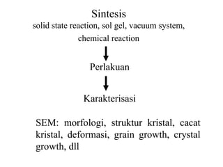
- 1. Sintesis solid state reaction, sol gel, vacuum system, chemical reaction Perlakuan Karakterisasi SEM: morfologi, struktur kristal, cacat kristal, deformasi, grain growth, crystal growth, dll
- 4. Skema SEM
- 5. General Uses: •Mengamati permukaan pada M= 10-100000 X, resolusi permukaan hingga kedalaman 3-100 nm •Apabila ditambahkan dengan detektor backscattered, SEM berfungsi untuk:(1) mengamati grain boundaries pada sampel tanpa etsa; (2)pengamatan daerah domain pada material ferromagnetic, (3)evaluasi orientasi kristalografi grain dengan diameter 2-10 m, (4)pengamatan fasa lain akibat adanya perbedaan rerata grain
- 6. Examples of Aplication • Pengamatan permukaan dengan perbesaran diatas perbesaran mikroskop optik • Pengamatan fracture surfaces dan perbedaan kedalaman permukaan akibat etsa • Penentuan orientasi kristalografi akibat preparasi surface, individual grain, fasa presipitat dan dendrite
- 7. • Identifikasi elemen kimia dalam ukuran mikron pada bulk sample,eg; inclusi, fasa presipitate • Evaluasi gradien komposisi kimia pada permukaan bulk sample • Pengamatan pada semikonduktor devices untuk failure analysis, function control dan verifikasi desain Examples of Aplication
- 8. Sampel • Form; solid ataupun liquid dengan tekanan rendah(>10-3 torr atau 0.13 Pa) • Size: dibatasi oleh kemampuan masing-masing peralatan biasanya sample dengan luasan 15-20 cm2 atau ukuran 4-8 cm masih mungkin diamati dengan SEM • Preparation: standar metalografi berupa teknik polishing dan etsa yang berlaku untuk material konduktif. Untuk material non-konduktif biasanya di-coating dengan lapisan tipis carbon, gold atau gold alloy hingga ketebalan lapisan 400Å. Sampel harus terhubung dengan holder biasanya digunakan pasta perak. Sample harus terbebas dari uap air, bahan pengotor organik dan minyak
- 9. Capabilities of related Techniques • X-ray Diffraction: menyediakan informasi kristalografi • Mikroskop Optik: memberikan informasi awal keadaan permukaan sampel • Transmission electron microscopy: memberikan informasi keadaan material secara spesifik; dislokasi, small angle boundari distribution and vacancy cluster.
- 11. Kategori komponen dalam mikroskop elektron 1. Electron column 2. Specimen chamber 3. Vacuum pumping system 4. Electronic control and imaging system
- 13. A Thermionic Electron Gun functions in the following manner 1. An positive electrical potential is applied to the anode 2. The filament (cathode) is heated until a stream of electrons is produced 3. The electrons are then accelerated by the positive potential down the column 4. A negative electrical potential (~500 V) is applied to the Whenelt Cap 5. As the electrons move toward the anode any ones emitted from the filament's side are repelled by the Whenelt Cap toward the optic axis (horizontal center) 6. A collection of electrons occurs in the space between the filament tip and Whenelt Cap. This collection is called a space charge 7. Those electrons at the bottom of the space charge (nearest to the anode) can exit the gun area through the small (<1 mm) hole in the Whenelt Cap 8. These electrons then move down the column to be later used in imaging
- 14. Parameter elektron gun Brightness, yang menunjukkan fungsi material filamen, suhu operasi dan tegangan. LaB6 adalah material dengan nilai tertinggi dimana nilainya 10-20 X lipat dibanding tungsten 2 2 4 / o o d I solidangle area current
- 15. • The Broers design utilizes a tungsten coil wrapped around the pointed end of a long (around 2 cm) LaB6 rod. This design uses the heat radiation and electron bombardment from the tungsten coil to heat the very end of the tip. The conduction of heat through the cathode holder, located at the other end of the rod, helps to lessen the problems of the reactivity of the material. • Vogel proposed a short LaB6 rod heated directly by passing a current through the LaB6 rod, perpendicular to the length of the rod. This is accomplished by using rigid electrical connectors that also provide the support for the rod. • In the design of Ferris et al.7, a short LaB6 rod is supported by a ribbon or strip through which an electrical current is passed for heating. The rod is heated by conduction from the ribbon.
- 17. Backscattered Electrons: Formation Caused by an incident electron colliding with an atom in the specimen which is nearly normal to the incident's path. The incident electron is then scattered "backward" 180 degrees. Utilization The production of backscattered electrons varies directly with the specimen's atomic number. This differing production rates causes higher atomic number elements to appear brighter than lower atomic number elements. This interaction is utilized to differentiate parts of the specimen that have different average atomic number. An example is shown in the SEM output section, specifically the mechanically alloyed specimen micrograph
- 18. Secondary Electrons: Source Caused by an incident electron passing "near" an atom in the specimen, near enough to impart some of its energy to a lower energy electron (usually in the K-shell). This causes a slight energy loss and path change in the incident electron and the ionization of the electron in the specimen atom. This ionized electron then leaves the atom with a very small kinetic energy (5eV) and is then termed a "secondary electron". Each incident electron can produce several secondary electrons. Utilization Production of secondary electrons is very topography related. Due to their low energy, 5eV, only secondaries that are very near the surface (<10nm) can exit the sample and be examined. Any changes in topography in the sample that are larger than this sampling depth will change the yield of secondaries due to collection efficiencies. Collection of these electrons is aided by using a "collector" in conjunction with the secondary electron detector. The collector is a grid or mesh with a +100V potential applied to it which is placed in front of the detector, attracting the negatively charged secondary electrons to it which then pass through the grid-holes and into the detector to be counted.
- 19. Auger Electrons Source Caused by the de-energization of the specimen atom after a secondary electron is produced. Since a lower (usually K-shell) electron was emitted from the atom during the secondary electron process an inner (lower energy) shell now has a vacancy. A higher energy electron from the same atom can "fall" to a lower energy, filling the vacancy. This creates and energy surplus in the atom which can be corrected by emitting an outer (lower energy) electron; an Auger Electron. Utilization Auger Electrons have a characteristic energy, unique to each element from which it was emitted from. These electrons are collected and sorted according to energy to give compositional information about the specimen. Since Auger Electrons have relatively low energy they are only emitted from the bulk specimen from a depth of <3
- 20. X-rays Source Caused by the de-energization of the specimen atom after a secondary electron is produced. Since a lower (usually K-shell) electron was emitted from the atom during the secondary electron process an inner (lower energy) shell now has a vacancy. A higher energy electron can "fall" into the lower energy shell, filling the vacancy. As the electron "falls" it emits energy, usually X-rays to balance the total energy of the atom so it . Utilization X-rays or Light emitted from the atom will have a characteristic energy which is unique to the element from which it originated. These signals are collected and sorted according to energy to yield micrometer diameter) of bulk specimens limiting the point-to-point comparisons available
- 21. Thin Specimen Interactions Unscattered Electrons Source Incident electrons which are transmitted through the thin specimen without any interaction occurring inside the specimen. Utilization The transmission of unscattered electrons is inversely proportional to the specimen thickness. Areas of the specimen that are thicker will have fewer transmitted unscattered electrons and so will appear darker, conversely the thinner areas will have more transmitted and thus will appear lighter.
- 22. Elasticity Scattered electrons Source Incident electrons that are scattered (deflected from their original path) by atoms in the specimen in an elastic fashion (no loss of energy). These scattered electrons are then transmitted through the remaining portions of the specimen. Utilization All electrons follow Bragg's Law and thus are scattered according to Wavelength=2*Space between the atoms in the specimen*sin(angle of scattering). All incident electrons have the same energy(thus wavelength) and enter the specimen normal to its surface. All incidents that are scattered by the same atomic spacing will be scattered by the same angle. These "similar angle" scattered electrons can be collated using magnetic lenses to form a pattern of spots; each spot corresponding to a specific atomic spacing (a plane). This pattern can then yield information about the orientation, atomic arrangements and phases present in the area being examined.
- 23. Inelastically Scattered Electrons Source Incident electrons that interact with specimen atoms in a inelastic fashion, loosing energy during the interaction. These electrons are then transmitted trough the rest of the specimen Utilization Inelasticaly scattered electrons can be utilized two ways •Electron Energy Loss Spectroscopy: The inelastic loss of energy by the incident electrons is characteristic of the elements that were interacted with. These energies are unique to each bonding state of each element and thus can be used to extract both compositional and bonding (i.e. oxidation state) information on the specimen region being examined. •Kakuchi Bands: Bands of alternating light and dark lines that are formed by inelastic scattering interactions that are related to atomic spacings in the specimen. These bands can be either measured (their width is inversely proportional to atomic spacing) or "followed" like a roadmap to the "real" elasticity scattered electron pattern.
- 25. Pemasangan detektor This is an image of the broken surface of a piece of metal, formed using secondary electron imaging This is a picture taken inside the sample chamber. On the left of the secondary detector is the lens, on the right is the backscatter detector.
- 26. Pemasangan detektor On the far left of the backscatter detector is the lens, in the center is the secondary detector. To collect electrons, the backscatter detector moves under the lens so the electron beam can travel through the hole in its center. This is an image of an aluminum copper alloy formed using backscattered electron imaging. The light area is mostly copper and the dark area is mostly aluminum.
- 27. Keseluruhan detektor pada SEM
- 28. Sistem Detektor • Detektor Secondary Electron (SE) untuk menghasilkan gambar analisis struktur mikro, analisis produk korosi, patahan, kegagalan material • Detektor Backscattered Electron (BSE) untuk menghasilkan gambar topografi peta struktur mikro yang gambarnya dibentuk dari perbedaan nomor atom/densitas yang dikandung oleh bahan. Daerah cuplikan dengan nomer atom yang lebih tinggi akan terlihat relatif lebih terang daripada daerah dengan nomer atom rendah • Detektor sinar-x (SiLi) dan EDX/EDS untuk analisis komposisi unsur yang terkandung dalam orde micrometer dan pemetaan (distribusi unsur) dalam suatu bahan