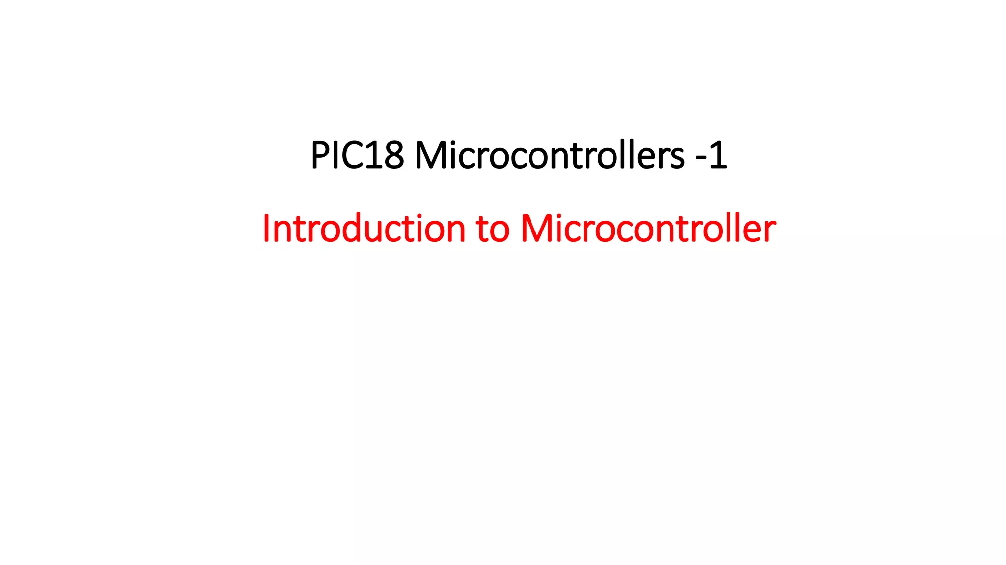
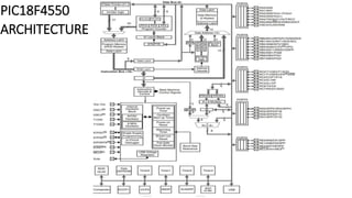
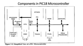
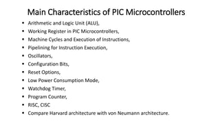
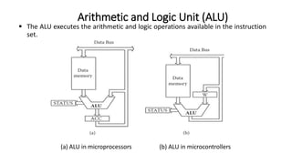
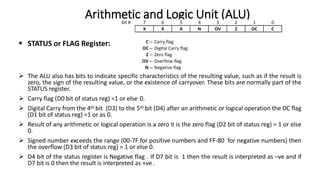
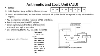
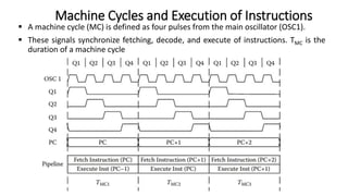
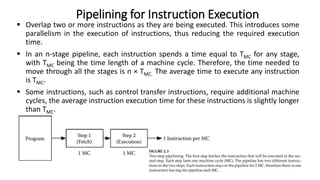
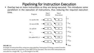
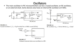
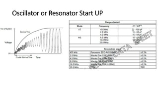
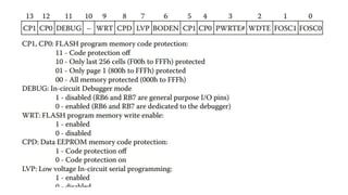
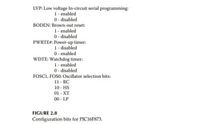
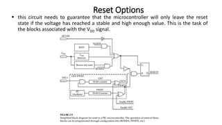
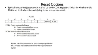
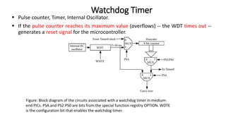
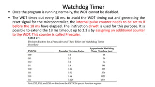
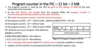
The document discusses the architecture and components of PIC18 microcontrollers. It describes the arithmetic logic unit (ALU) and its associated registers. It explains machine cycles, instruction execution, and pipelining. It also covers oscillators, configuration bits, reset options, low power modes, watchdog timers, and the program counter. It compares Harvard and von Neumann architectures.

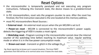
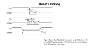
![ The OST/PWRT, oscillator start-up timer (OST), and power-up timer (PWRT). It takes
a certain amount of time for the main oscillator to reach stable values for its
frequency and amplitude after it has been turned on.
power-up timer (PWRT): An internal RC oscillator, independent of the main
oscillator, introduces a 72 ms delay to the signal PWRT after the oscillator has been
powered. ]
oscillator start-up timer (OST): The OST introduces an additional delay of 1024
pulses. This delay is long enough for the oscillator to reach stable amplitude and
frequency values. The OST starts its operation only after the PWRT has reached its
maximum value.
Reset Options
Figure: Time diagrams showing the sequence of signals
associated with the OST/PWRT block. (a)
Power-on reset—MCLR# pin connected to VDD](https://image.slidesharecdn.com/lectureonpic-1-230419052758-8c154095/85/Lecture-on-PIC-1-pptx-22-320.jpg)
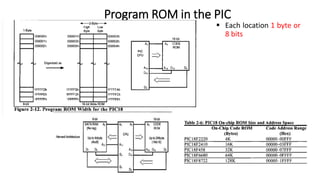
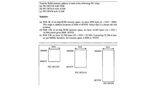
![Program memory (ROM) for PIC18 family
[1] Fernando E. Valdes-Perez, Ramon Pallas-Areny, “Microcontrollers - Fundamentals and Applications with PIC”, CRC Press, 1st Edition, 2009
[2] Mazidi M. A., McKinlay R. D., Causey D., “PIC Microcontroller And Embedded Systems.”, Pearson Education International, 2008
[3] https://ww1.microchip.com/downloads/en/devicedoc/39632c.pdf](https://image.slidesharecdn.com/lectureonpic-1-230419052758-8c154095/85/Lecture-on-PIC-1-pptx-32-320.jpg)


![[Deck] What's New in Spark-Iceberg Integration via DSV2.pptx](https://cdn.slidesharecdn.com/ss_thumbnails/deckwhatsnewinspark-icebergintegrationviadsv2-260210005337-25955b12-thumbnail.jpg?width=640&height=640&fit=bounds)


