Downloaded 188 times

![1.4 Measurement Units and Applications
All dimensions and tolerances, as well as other forms of measurement
(temperature, weight, etc.) in this standard are expressed in SI (System
International) units (with Imperial English equivalent dimensions
provided in brackets). Dimensions and tolerances use millimeters as
the main form of dimensional expression; micrometers are used when
the precision required makes millimeters too cumbersome. Celsius is
used to express temperature. Weight is expressed in grams.
This Standard uses International System of Units (SI) units per ASTM
SI10-10, IEEE/ASTM SI 10 Practice (Section 3) [Imperial English
equivalent units are in brackets for convenience]. The SI units used in
this Standard are millimeters (mm) [in] for dimensions and
dimensional tolerances, Celsius (°C) [°F] for temperature and
temperature tolerances, grams (g) [oz] for weight, lux (lx) [footcandles]
for illuminance.
Note: This Standard uses other SI prefixes (ASTM SI10-10, Section 3.2)
to eliminate leading zeroes (for example, 0.0012 mm becomes 1.2 μm)
or as alternative to powers-of-ten (3.6 × 10³ mm becomes 3.6 m).
© 2018 BEST Inc. - Presented for SMTA 1-29-18](https://image.slidesharecdn.com/smtawebinarj-std-001revf-gcomparison-180131211054/85/J-STD-001-IPC-A-610-F-to-G-Differences-Webinar-4-320.jpg)
![3.1 Materials
Manufacturers, when specified, shall [N1N2D3]
have a lead-free control plan (LFCP), which shall
[N1N2D3] be agreed upon by the Manufacturer
and the User.
Note: GEIA-STD-0005-1 and GEIA-STD-0005-2
constitute examples for the implementation of
LFCPs/tin whisker mitigation for Aerospace and
other High Performance Electronic Systems.
© 2018 BEST Inc. - Presented for SMTA 1-29-18](https://image.slidesharecdn.com/smtawebinarj-std-001revf-gcomparison-180131211054/85/J-STD-001-IPC-A-610-F-to-G-Differences-Webinar-11-320.jpg)
![3.2.2.1 Solder Pot Purity and Maintenance
Dross shall [N1D2D3] be removed from the
solder surface in a manner that assures the
dross does not contact the items being tinned.
© 2018 BEST Inc. - Presented for SMTA 1-29-18](https://image.slidesharecdn.com/smtawebinarj-std-001revf-gcomparison-180131211054/85/J-STD-001-IPC-A-610-F-to-G-Differences-Webinar-12-320.jpg)
![4.1 Electrostatic Discharge (ESD)
If there are any assemblies that contain
components or parts sensitive to ESD, the
Manufacturer shall [D1D2D3] implement a
documented ESD control program in accordance
with ANSI/ESD S20.20, IEC 61340-5-1, MIL-STD-
1686, or as agreed between User and Supplier.
Documentation necessary for an effective
program shall [D1D2D3] be available for review.
© 2018 BEST Inc. - Presented for SMTA 1-29-18](https://image.slidesharecdn.com/smtawebinarj-std-001revf-gcomparison-180131211054/85/J-STD-001-IPC-A-610-F-to-G-Differences-Webinar-13-320.jpg)
![4.2 Facilities
Cleanliness and ambient environments in all
work areas shall [D1D2D3] be maintained at
levels that prevent contamination or
deterioration of tools, materials, and surfaces to
be soldered or conformally coated. Eating,
drinking, smoking, including use of e-cigarettes,
and/or use of tobacco products shall [D1D2D3]
be prohibited in the work area.
© 2018 BEST Inc. - Presented for SMTA 1-29-18](https://image.slidesharecdn.com/smtawebinarj-std-001revf-gcomparison-180131211054/85/J-STD-001-IPC-A-610-F-to-G-Differences-Webinar-14-320.jpg)
![4.6 Thermal Protection
Multilayer Ceramic Chip Capacitors (MLCCs) and
‘‘stacked’’ capacitors containing these parts
shall [N1D2D3] be handled as thermal shock
sensitive. Heat up and cool down rates should
be controlled within the component
manufacturer's recommendations.
© 2018 BEST Inc. - Presented for SMTA 1-29-18](https://image.slidesharecdn.com/smtawebinarj-std-001revf-gcomparison-180131211054/85/J-STD-001-IPC-A-610-F-to-G-Differences-Webinar-15-320.jpg)
![4.9 General Part Mounting Requirements
Uninsulated parts mounted over exposed
circuitry shall [N1N2D3] have their leads formed
to provide a minimum of 0.25 mm [0.01 in]
between the bottom of the component body
and the exposed circuitry.
© 2018 BEST Inc. - Presented for SMTA 1-29-18](https://image.slidesharecdn.com/smtawebinarj-std-001revf-gcomparison-180131211054/85/J-STD-001-IPC-A-610-F-to-G-Differences-Webinar-16-320.jpg)

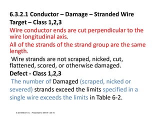
![5.1.2 Strand Damage
The number of damaged (nicked or broken) strands in a
wire shall not [D1D2D3] exceed the limits given in Table
5-1. There shall not [N1P2P3] be any number of severed
or damaged strands less than the quantity allowed in
Table 5-1. There shall [A1P2D3] be no strand separation
(birdcaging) greater than one strand diameter. There shall
[A1D2D3] be no strand separation (birdcaging) beyond
the outside diameter of the insulation. Recommendations
and requirements on wires used in high voltage
applications are provided in 1.13.2.3.
• Wire strands shall not [A1D2D3] be altered or cut to fit
terminals.
© 2018 BEST Inc. - Presented for SMTA 1-29-18](https://image.slidesharecdn.com/smtawebinarj-std-001revf-gcomparison-180131211054/85/J-STD-001-IPC-A-610-F-to-G-Differences-Webinar-20-320.jpg)
![5.1.3.2 Tinning of Stranded Wire – Coverage
The solder shall [N1D2D3] wet the tinned
portion of the wire and should penetrate to the
inner strands of the wire. Pinholes, voids,
dewetting/nonwetting shall not [A1P2D3]
exceed 5% of the area required to be tinned.
© 2018 BEST Inc. - Presented for SMTA 1-29-18](https://image.slidesharecdn.com/smtawebinarj-std-001revf-gcomparison-180131211054/85/J-STD-001-IPC-A-610-F-to-G-Differences-Webinar-21-320.jpg)
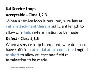
![5.4.1.2 Service Loops
When service loops are required at initial
attachment, wires shall [D1D2D3] have
sufficient length as shown in Figure 5-6, 7 to
allow at least one field re-termination.
Note: When Service Loop(s) are required, that
requirement should be included on the
assembly drawing(s)/documentation.
© 2018 BEST Inc. - Presented for SMTA 1-29-18](https://image.slidesharecdn.com/smtawebinarj-std-001revf-gcomparison-180131211054/85/J-STD-001-IPC-A-610-F-to-G-Differences-Webinar-22-320.jpg)
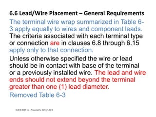
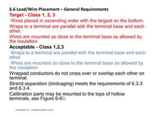
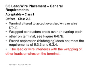
![5.4.1.4 Orientation of Lead or Wire Wrap
Attachments to terminals that require a wrap
may be wrapped clockwise or counterclockwise
(consistent with the direction of potential stress
application). The lead or wire shall [A1P2D3]
continue the curvature of the dress of the
lead/wire. Wrapped conductors shall not
[A1D2D3] cross over or overlap themselves or
each other on the terminal. and shall not
[A1D2D3] interfere with the wrapping of other
leads or wires on the terminal or overlap itself.
© 2018 BEST Inc. - Presented for SMTA 1-29-18](https://image.slidesharecdn.com/smtawebinarj-std-001revf-gcomparison-180131211054/85/J-STD-001-IPC-A-610-F-to-G-Differences-Webinar-23-320.jpg)
![5.4.1.5 Continuous Runs A continuous solid bus wire may be run from
terminal to terminal to three or more bifurcated, turret, or pierced
terminals are to be connected. A curvature shall [D1D2D3] be
included in the unwrapped wire portion of the jumper to provide relief
of tension from environmental loading. The connections to the first
and last terminals shall [D1D2D3] meet the required wrap for
individual terminals.
The following additional requirements shall [A1P2D3] be met:
a. For each intermediate turret terminal, the wire is wrapped 3600
around or interweaves each terminal.
b. For each intermediate bifurcated terminal, the wire passes
through the slot and is in contact with the base of the terminal or a
previously installed wire.
c. For each intermediate pierced or perforated terminal, the wire is
in contact with at least two nonadjacent contact surfaces of each
intermediate terminal.
d. For each intermediate hook terminal, the wire is wrapped 360°
around each terminal.
© 2018 BEST Inc. - Presented for SMTA 1-29-18](https://image.slidesharecdn.com/smtawebinarj-std-001revf-gcomparison-180131211054/85/J-STD-001-IPC-A-610-F-to-G-Differences-Webinar-24-320.jpg)
![5.4.3.1 Side Route Connection
Table 5-6 provides the staking criteria for side route
connections that do not meet minimum wrap criteria, see
Figure 5-10. As an alternative to the wrap criteria
provided in Table 5-5, wire(s) and/or component lead(s)
may be routed straight through the terminal when the
assembly drawing/documentation incorporates
bonding/staking for the wire(s)/lead(s) to the
requirements of Table 5-6. If straight through routing is
utilized, wire(s) or lead(s) shall [A1P2D3] extend beyond
the post of the terminal and be in contact with the base
of the terminal or the previously installed wire (see Figure
5-11). Additionally, wires/leads shall [D1D2D3] meet the
staking requirements of Table 5-6.
© 2018 BEST Inc. - Presented for SMTA 1-29-18](https://image.slidesharecdn.com/smtawebinarj-std-001revf-gcomparison-180131211054/85/J-STD-001-IPC-A-610-F-to-G-Differences-Webinar-25-320.jpg)
![9.1.12 Crazing Crazing shall not [N1D2D3]
exceed 50% of the physical spacing between
noncommon conductors.
Crazing at the edge of the board shall not
N1D2D3] reduce the spacing minimum defined
distance between the board edge and any
conductive pattern to below the minimum
lateral conductor spacing specified in the
drawing(s)/documentation. If the minimum
distance is not specified, crazing shall not
[N1D2D3] reduce the distance between the
board edge and conductive pattern by not more
than 50% or 2.5 mm [0.1 in], whichever is less.
© 2018 BEST Inc. - Presented for SMTA 1-29-18](https://image.slidesharecdn.com/smtawebinarj-std-001revf-gcomparison-180131211054/85/J-STD-001-IPC-A-610-F-to-G-Differences-Webinar-27-320.jpg)
![10 COATING, ENCAPSULATION AND STAKING (ADHESIVE)
All assemblies shall [N1N2D3] be clean before processing. After
cleaning, prior to processing, assemblies shall [N1N2D3] be handled to
prevent contamination. The material specification/data sheet or other
documented procedure shall [D1D2D3] be followed for mixing and
curing. The material shall [D1D2D3] be used within the time period
specified (both shelf life and pot life) or used within the time period
indicated by a documented system to control age-dated material.
When processing varies from supplier recommended instructions, the
variations shall [D1D2D3] be documented and available for review.
Items exposed to uncured silicone material shall not [D1D2D3] be
used for processing other material. An authorized exception is allowed
only in cases where equipment is used for co-curing processes and the
manufacturer has demonstrated through system tests that non-
silicone material properties have not changed and design
requirements are met. Objective evidence shall [D1D2D3] be
maintained and available for review.
© 2018 BEST Inc. - Presented for SMTA 1-29-18](https://image.slidesharecdn.com/smtawebinarj-std-001revf-gcomparison-180131211054/85/J-STD-001-IPC-A-610-F-to-G-Differences-Webinar-28-320.jpg)
![10.5.1.2 Staking – Application - SMT The following criteria apply to surface mount
components only.
a. Components whose longest dimension is their height - The staking material shall
[N1D2D3] be applied to a minimum height of 25% of each individual component’s
body height. Slight flow of staking material under the component body is acceptable
provided it does not violate 10.5.1.
i. For closely spaced arrays consisting of up to four components fillet height
requirements for the two outer end-faces shall [N1D2D3] be the same as for an
individual component. In addition, the top inner surfaces shall [N1D2D3] be bonded
to each other for 50% of the components’ width.
ii. For closely spaced arrays consisting of greater than four components staking
shall [N1D2D3] be applied in the same manner as arrays up to four components, with
the additional requirement that every other internal component shall [N1D2D3] have
their sides staked to the board surface.
b. Components whose longest dimension is their diameter or length (e.g., QFPs)
Rectangular components shall [N1D2D3] be staked with a bead of staking material
placed at each corner of the component. For each bead, the staking material shall
[N1D2D3] contact a minimum 25% of the height of the component body. Slight flow of
staking material under the component body is acceptable provided it does not violate
© 2018 BEST Inc. - Presented for SMTA 1-29-18](https://image.slidesharecdn.com/smtawebinarj-std-001revf-gcomparison-180131211054/85/J-STD-001-IPC-A-610-F-to-G-Differences-Webinar-29-320.jpg)
![12.1.2 Visual Inspection The assembly shall [N1D2D3]
be evaluated either by sample based inspection in
accordance with the established a documented process
control plan system, see 12.2, or by 100% visual
inspection, see 1.11. Inspection of soldering and post
solder cleanliness may be performed in the same
operation using Tables 12-1, 12-2, and 12-3 conformal
coating, staking or encapsulation shall [N1D2D3] be
performed after and not combined with, soldering and
cleaning process inspections. Inspection of soldering and
cleanliness shall [N1D2D3] be performed prior to
conformal coating, staking or encapsulation. Inspection
for damage may be combined with solder and/or
cleanliness inspections. Inspection for damage should be
performed prior to conformal coating and as part of the
final inspection process.
© 2018 BEST Inc. - Presented for SMTA 1-29-18](https://image.slidesharecdn.com/smtawebinarj-std-001revf-gcomparison-180131211054/85/J-STD-001-IPC-A-610-F-to-G-Differences-Webinar-30-320.jpg)

![1.4 Measurement Units and Applications This Standard uses International System of
Units (SI) units per ASTM SI10-10, IEEE/ASTM SI 10 American National Standard for
Metric Practice (Section 3) [Imperial English equivalent units are in brackets
forconvenience]. The SI units used in this Standard are millimeters (mm) [in] for
dimensions and dimensional tolerances, Celsius (°C) [°F] for temperature and
temperature tolerances, grams (g) [oz] for weight, lux (lx) [footcandles] for
illuminance.
Note: This Standard uses other SI prefixes (ASTM SI10-10, Section 3.2) to eliminate
leading zeroes (for example, 0.0012 mm becomes 1.2 μm) or as alternative to powers-
of-ten (3.6 × 10³ mm becomes 3.6 m).
1.4.1 Verification of Dimensions Actual MeasurementsFor determining conformance
to the specifications in this Standard, round all observed or calculated values “to the
nearest unit” in the last right-hand digit used in expressing the specification limit, in
accordance with the
• J-STD-001G Draft Document for Industry Consensus Ballot Only January 2017
• 2 | P a g e
• rounding method of ASTM Practice E29, Using Significant Digits in Test Data to
Determine Conformance with Specification. For
• example, specifications of 2.5 mm max, 2.50 mm max, or 2.500 mm max, round
the measured value to the nearest 0.1 mm, 0.01 mm,
• or 0.001 mm, respectively, and then compare to the specification number cited.
© 2018 BEST Inc. - Presented for SMTA 1-29-18](https://image.slidesharecdn.com/smtawebinarj-std-001revf-gcomparison-180131211054/85/J-STD-001-IPC-A-610-F-to-G-Differences-Webinar-33-320.jpg)
![4.1.5 Hardware Installation - Threaded Fasteners and
Other Threaded Hardware
Acceptable - Class 1
Defect – Class 2,3
Less than one and one-half threads extend beyond the
threaded hardware, (e.g., nut) unless otherwise specified
by engineering drawing. thread extension would interfere
with other component.
Thread extension more than 3 mm [0.1 in] plus one and
one-half threads for bolts or screws up to 25 mm [1 in].
Thread extension more than 6.3 mm [0.25 in] plus one
and one-half threads for bolts or screws over 25 mm [1
in]. Bolts or screws without locking mechanisms extend
less than one and one half threads beyond the threaded
hardware.
© 2018 BEST Inc. - Presented for SMTA 1-29-18](https://image.slidesharecdn.com/smtawebinarj-std-001revf-gcomparison-180131211054/85/J-STD-001-IPC-A-610-F-to-G-Differences-Webinar-40-320.jpg)
![4.2 Jackpost Mounting
This section covers the height relationship of the face of the jackpost to the associated
connector face. This is critical to obtain maximum connector pin contact.
Hardware stack-up for mounted connectors may be varied in order to locate the face
of the jackpost flush to 0.75 mm [0.030in] below the face of the connector.
Acceptable - Class 1,2,3
Jackpost face is flush to 0.75 mm [0.030 in] below the face of the connector.
The jackposts can be above or below the face of the connector, depending on
the design, providing the connector and jackposts mate
correctly.
Height is obtained by adding or removing washers
(supplied with jackpost) in accordance with manufacturer’s instructions.
Defect - Class 1,2,3
Jackpost face extends above the connector face, see Figure 4-28 The jackposts are
above or below the face of the connector, depending on the design, and the
connector and jackposts do not mate correctly. (No figure showing the defect
condition.).
Face of jackpost is greater than 0.75 mm [0.030 in] below the connector face, see
Figure 4-29.
© 2018 BEST Inc. - Presented for SMTA 1-29-18](https://image.slidesharecdn.com/smtawebinarj-std-001revf-gcomparison-180131211054/85/J-STD-001-IPC-A-610-F-to-G-Differences-Webinar-43-320.jpg)
![6.2.3.1 Insulation - Flexible Sleeve – Placement
Acceptable – Class 2,3
• Sleeving/tubing is tight on terminal and
wire/cable.
• Multiple pieces of sleeving overlap each other by
at least 3 wire/cable diameters, or 13 mm [0.5in],
whichever is larger.
Defect – Class 2,3
• Sleeving/tubing is not tight on terminal and
wire/cable.
• Multiple pieces of sleeving overlap is less than 3
• wire/cable diameters or 13 mm [0.5
inch],whichever is less.
© 2018 BEST Inc. - Presented for SMTA 1-29-18](https://image.slidesharecdn.com/smtawebinarj-std-001revf-gcomparison-180131211054/85/J-STD-001-IPC-A-610-F-to-G-Differences-Webinar-47-320.jpg)
![6.9.1 Bifurcated - Lead/Wire Placement - Side Route Attachments
Acceptable - Class 1
Process Indicator - Class 2
Defect - Class 3
• Any portion of the wrap extends beyond the top of
• terminal post.
• Wire does not have positive contact with at least one corner of the
post.
• Wire/lead less than 0.75 mm [0.03 in] in diameter is wrapped
around a post less than 90º.
Defect - Class 1,2,3
• Wire does not pass through slot.
• Wire end violates minimum electrical clearance, see Figure 6-82.
• Wire/lead less than 0.75 mm [0.03 in] in diameter is wrapped around a
post less than 90º and is not staked, see 6.9.2.
© 2018 BEST Inc. - Presented for SMTA 1-29-18](https://image.slidesharecdn.com/smtawebinarj-std-001revf-gcomparison-180131211054/85/J-STD-001-IPC-A-610-F-to-G-Differences-Webinar-55-320.jpg)
![7.3.5.1 Supported Holes – Solder - Vertical fill (A)
Acceptable - Class 2
• Minimum vertical fill of 50% or 1.2 mm [0.05in],
whichever is less, for components with 14 (not
shown).
• Component lead is discernible in the solder source
side of the solder connection.
• Minimum vertical fill of hole is more than 50% or
1.2 mm [0.05 in], whichever is less, for
components with less than 14 leads and having
an internal thermal plane providing the solder fillet
of Side B of Figure 7-87 has wetted 360o of the
PTH barrel wall and 360o of the lead and the
surrounding PTHs meet requirements of Table 7-4.
© 2018 BEST Inc. - Presented for SMTA 1-29-18](https://image.slidesharecdn.com/smtawebinarj-std-001revf-gcomparison-180131211054/85/J-STD-001-IPC-A-610-F-to-G-Differences-Webinar-58-320.jpg)
![Defect - Class 2
• Vertical fill of hole is less than 75% for
component less than 14 leads and not having an
internal thermal plane.
• Vertical fill of hole is less than 75% and greater
than 50% or 1.2 mm [0.05 in], whichever is less,
for components with less than 14 leads and
having an internal thermal plane and the solder
fillet on Side B of Figure 7-867 has wetted less
than 360° of the PTH barrel wall and less than
360° of the lead.
• Vertical fill of hole is less than 50% or 1.2
mm[0.05 in], whichever is less, for component
with greater than or equal to 14 leads or more.
© 2018 BEST Inc. - Presented for SMTA 1-29-18](https://image.slidesharecdn.com/smtawebinarj-std-001revf-gcomparison-180131211054/85/J-STD-001-IPC-A-610-F-to-G-Differences-Webinar-60-320.jpg)
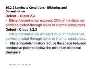
![10.2.4 Laminate Conditions – Haloing
Acceptable - Class 1,2,3
• The distance between the haloing penetration and the
nearest conductive feature is not less than the
minimum lateral conductor spacing, or 0.1 mm [0.004 in]
when the minimum lateral conductor spacing is not
specified.
• Defect - Class 1,2,3
• The distance of between the haloing penetration and
the nearest conductive feature is less than the
minimum lateral conductor spacing, or less than 0.1
mm [0.004 in] when the minimum lateral conductor
spacing is not specified.
© 2018 BEST Inc. - Presented for SMTA 1-29-18](https://image.slidesharecdn.com/smtawebinarj-std-001revf-gcomparison-180131211054/85/J-STD-001-IPC-A-610-F-to-G-Differences-Webinar-68-320.jpg)
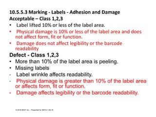
![10.4.2.2 Flexible and Rigid-Flex Printed Circuitry –Delamination/Blister – Flex to Stiffener
Not Established – Class 1
Acceptable – Class 2,3
• The distance from stiffener board edge in the straight section of flex circuit which is
intended to remain straight is 0.5mm [0.02 in] or less.
• The distance from stiffener board edge in the bend section of the flex circuit which is
intended to bend is 0.3mm [0.01 in] or less.
• The area of blister or delamination between flex circuitry and a stiffener board exceeds
20% of the joined area provided the thickness of the blister does not exceed the thickness
limit of the entire board.
• Delamination (separation) or bubbles in the coverlayers of the flexible circuitry does not
span more than 25% of the distance between adjacent conductive patterns.
• Not Established – Class 1
• Defect – Class 2,3
• The distance from stiffener board edge in the straight section of flex circuit which is
intended to remain straight exceeds 0.5mm [0.02 in].
• The distance from stiffener board edge in the bend section exceeds 0.3mm [0.01 in].
• The area of blister or delamination between flex circuitry and a stiffener board
exceeds 20% of the joined area.
• Delamination (separation) or bubbles in the coverlayers of the flexible circuitry span more
than 25% of the distance between adjacent conductive patterns.
© 2018 BEST Inc. - Presented for SMTA 1-29-18](https://image.slidesharecdn.com/smtawebinarj-std-001revf-gcomparison-180131211054/85/J-STD-001-IPC-A-610-F-to-G-Differences-Webinar-69-320.jpg)

The document outlines standards, practices, and requirements for manufacturing soldered electrical and electronic assemblies, emphasizing quality control and conformity to specifications. It details materials, methods, acceptance criteria, and emphasizes the importance of using SI units for measurements. Additionally, it includes guidelines for component placement, soldering, and handling to maintain standards and prevent contamination during the manufacturing process.


