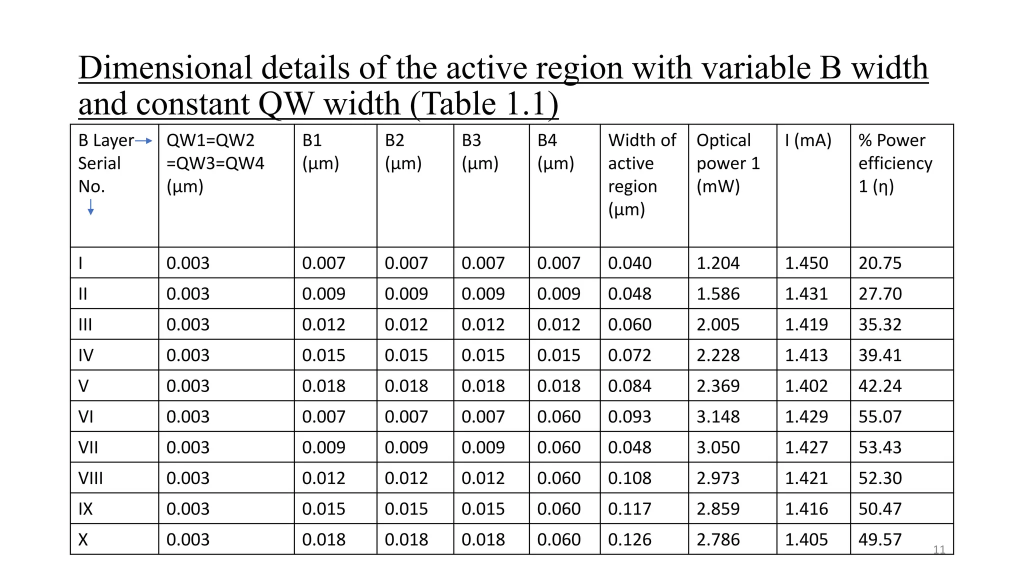
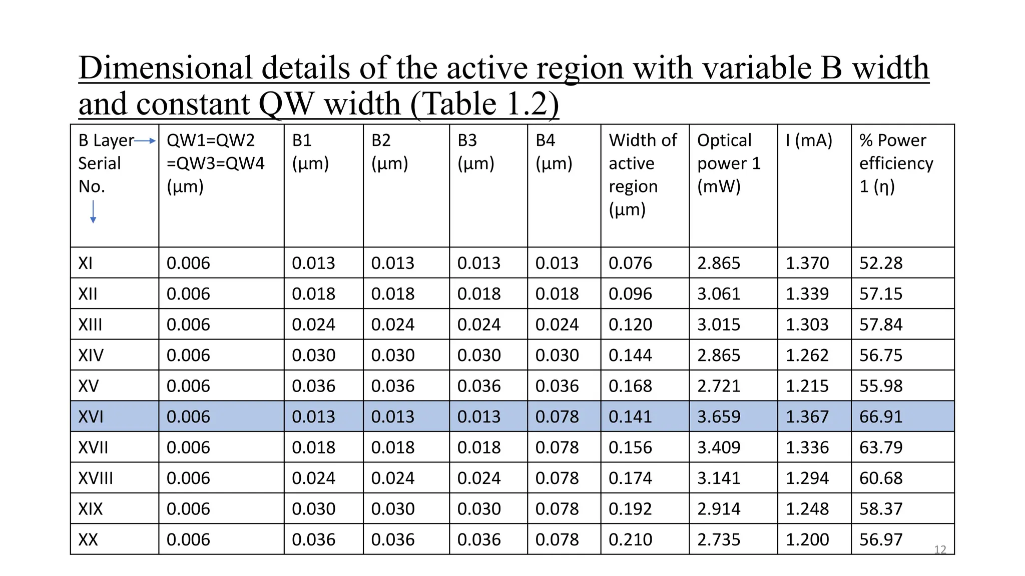
Numerical Investigation of Optoelectronic
Device to Enhance its Efficiency
Outline
What is optoelectronics?
Major optoelectronic devices.
Current trend on optoelectronic devices.
2
What Did the Word “Opto-Electronics”
Mean?
 Optoelectronics is the study and application of electronic devices
that interact with light.
3
Fig:1 []
Flowchart of Optoelectronic Devices
4
Flowchart:1
Examples of Optoelectronic Devices
5
Fig:2.5
Fig:2.1 Fig:2.2 Fig:2.3
Fig:2.4 Fig:2.6
Light-Emitting Diodes (LEDs)
Fig:3.1 [1]
Light-emitting diode (LED) is a
semiconductor diode that emits
incoherent narrow-spectrum light
when electrically biased in the forward
direction of the p-n junction.
6
Fig:3.2 [1]
Flowchart of Laser/LED Simulation
7
Flowchart:2
3µm
SiO2
Length~ 5µm
Substrate
Width~
3.5um
AlGaN
AlGaN
AlGaN
AlGaN
AlGaAs
GaAs
GaN
GaN
GaN
GaN
AlGaAs
Materials
GaAs
AlGaAs; X=0.1
AlGaAs; X=0.2
SiO2
Electrode
GaN
n-Contact
1µm
3µm
p-Contact
Active Region
0.1µm
0.1µm
0.1µm
Schematic Structure of LED
Fig:4.2 Exploded Structure of an Ideal LED
Fig:4.1 Schematic design of the GaN MQW LED structure [1]
Ratio and Range of width of QW to Barrier Layer in 4-layer
MQW GaN LED Structure
Positioning of quantum well and barrier layer in a GaN/AlGaN-based multi-
quantum well structure.
QW=Quantum Well width ; B = Barrier width
• In the first case, the width of the QW layers is kept constant, and the width of the
B layers varies.
• In the second case, both the QW and B layer widths are varied.
6/3/2024 Malaviya National Institute of Technology 9
Flowchart of the proposed design.
10
Variation in width of
QW and B Layers
Variable B and
Fixed QW;
Case 1
QW1=QW2=QW3=
QW4=QW=
0.003 µm ;
Case 1.1
B1 =B2 =B3
=B4=B;
6 QW ≥ B ≥ 2.2
QW
Table 1.1 (Design I-
V)
B1= B2= B3=
B≠B4;
B4 = 0.060 µm
6 QW ≥ B ≥ 2.2QW
Table 1.1 (Design
VI-X)
QW1=QW2=QW3=
QW4=QW= 0.006
µm ;
Case 1.2
B1=B2=B3=B4=B;
6 QW ≥ B ≥ 2.2
QW;
Table 1.2 (Design
XI-XV)
B1=B2=B3=B≠B4;
B4=0.078 µm;
Table 1.2 (Design
XVI-XX)
Variable QW (B
automatically
changes);
Case 2
QW1=0.010 µm &
B1=0.025 µm;
B1+B2+B3+B4= 0.121
µm;
0.021 µm
≥B2=B3≥0.003 µm;
B4=0.121-B2+B3
Flowchart:3
Dimensional details of the active region with variable B width
and constant QW width (Table 1.1)
B Layer
Serial
No.
QW1=QW2
=QW3=QW4
(μm)
B1
(μm)
B2
(μm)
B3
(μm)
B4
(μm)
Width of
active
region
(μm)
Optical
power 1
(mW)
I (mA) % Power
efficiency
1 (η)
I 0.003 0.007 0.007 0.007 0.007 0.040 1.204 1.450 20.75
II 0.003 0.009 0.009 0.009 0.009 0.048 1.586 1.431 27.70
III 0.003 0.012 0.012 0.012 0.012 0.060 2.005 1.419 35.32
IV 0.003 0.015 0.015 0.015 0.015 0.072 2.228 1.413 39.41
V 0.003 0.018 0.018 0.018 0.018 0.084 2.369 1.402 42.24
VI 0.003 0.007 0.007 0.007 0.060 0.093 3.148 1.429 55.07
VII 0.003 0.009 0.009 0.009 0.060 0.048 3.050 1.427 53.43
VIII 0.003 0.012 0.012 0.012 0.060 0.108 2.973 1.421 52.30
IX 0.003 0.015 0.015 0.015 0.060 0.117 2.859 1.416 50.47
X 0.003 0.018 0.018 0.018 0.060 0.126 2.786 1.405 49.57 11
Dimensional details of the active region with variable B width
and constant QW width (Table 1.2)
B Layer
Serial
No.
QW1=QW2
=QW3=QW4
(μm)
B1
(μm)
B2
(μm)
B3
(μm)
B4
(μm)
Width of
active
region
(μm)
Optical
power 1
(mW)
I (mA) % Power
efficiency
1 (η)
XI 0.006 0.013 0.013 0.013 0.013 0.076 2.865 1.370 52.28
XII 0.006 0.018 0.018 0.018 0.018 0.096 3.061 1.339 57.15
XIII 0.006 0.024 0.024 0.024 0.024 0.120 3.015 1.303 57.84
XIV 0.006 0.030 0.030 0.030 0.030 0.144 2.865 1.262 56.75
XV 0.006 0.036 0.036 0.036 0.036 0.168 2.721 1.215 55.98
XVI 0.006 0.013 0.013 0.013 0.078 0.141 3.659 1.367 66.91
XVII 0.006 0.018 0.018 0.018 0.078 0.156 3.409 1.336 63.79
XVIII 0.006 0.024 0.024 0.024 0.078 0.174 3.141 1.294 60.68
XIX 0.006 0.030 0.030 0.030 0.078 0.192 2.914 1.248 58.37
XX 0.006 0.036 0.036 0.036 0.078 0.210 2.735 1.200 56.97 12
Dimensional details of the active region with variable QW and
B width (Table 2)
Serial No. QW2=QW3=QW
4 (μm) (x%
width w.r.t.1st
QW)
B2=B3
(μm)
B4
(μm)
Width of
active
region
(μm)
Optical
power 2
(mW)
I (mA) % Power
efficiency 2
(η) (Case 2)
I 0.001 (10%) 0.003 0.090 0.134 1.591 1.401 26.13
II 0.002 (20%) 0.005 0.086 0.137 2.776 1.412 37.62
III 0.003 (30%) 0.007 0.082 0.140 3.404 1.421 40.53
IV 0.004 (40%) 0.009 0.078 0.143 3.733 1.426 42.30
V 0.005 (50%) 0.011 0.074 0.146 3.903 1.427 44.40
VI 0.006 (60%) 0.013 0.070 0.149 3.903 1.421 43.23
VII 0.007 (70%) 0.015 0.066 0.152 3.873 1.418 43.08
VIII 0.008 (80%) 0.017 0.062 0.155 3.824 1.411 42.81
IX 0.009 (90%) 0.019 0.058 0.158 3.811 1.407 42.33
X 0.010 (100%) 0.021 0.054 0.161 1.591 1.391 26.13
13
Simulation Results & Discussion
14
Fig:5.1 [1]
Fig:5.2 [1]
To enhance the power efficiency of the MQW LED device, the modification of the physical dimension is
one of many possible alternatives. The increased benefit is both economic and simple, as with no
significant modification in the existing technology and infrastructure, the performance of the LED is
enhanced. For the GaN structure referred here is that the QW width range between 0.003 um and 0.006 um
generates better results. The B width should also be 2.2 times to 5–6 times the QW width.
Relative position and width of QW and Barrier in an
MQW Structure
• QW1=QW2=QW3=QW4 & B1=B2=B3<B4 (1)
•
𝑄𝑊1
𝐵1
=
𝑄𝑊2
𝐵2
=
𝑄𝑊3
𝐵3
>
𝑄𝑊4
𝐵4
(2)
•
𝑄𝑊1
𝐵1
≤
1
2.2
𝐾 &
𝑄𝑊4
𝐵4
≤
1
5
𝐾 (3)
where k is a constant, generally ≈1.
6/3/2024 Malaviya National Institute of Technology 15
Application of Designed LED Design
16
General and Optical Communication Systems
17
Integration of Machine Learning in
Optics/Photonics
18
Research Paper Title Publisher (Journal) &
Publishing Year
Objective Outcome/Conclusion
Teaching optics to a
machine learning network
[3].
Optica Publishing Group
(Optics Letters) & 2020
How harmonic oscillator
equations can be
integrated in a neural
network to improve the
spectral response
prediction for an optical
system.
Artificial Intelligence and
Machine Learning in
Optical Information
Processing: introduction
to the feature issue [4].
Optica Publishing Group
(Applied Optics) & 2022
Ongoing and Future Scope
19
References
20
[1] Schubert, E. LED basics: Optical properties. In Light-Emitting Diodes (pp. 86-100). Cambridge: Cambridge
University Press, (2006).
[2] Sharma, L. and Sharma, R., "Design and Analytical Calculations of the Width and Arrangement of Quantum
Well and Barrier Layers in GaN/AlGaN LED to Enhance The Performance", Opto-Electronics Review, 29(4),
141-147 (2021).
[3] André-Pierre Blanchard-Dionne and Olivier J. F. Martin, "Teaching optics to a machine learning network,"
Opt. Lett. 45, 2922-2925 (2020).
[4] Khan Iftekharuddin, Chrysanthe Preza, Abdul Ahad S. Awwal, and Michael E. Zelinski, "Artificial
Intelligence and Machine Learning in Optical Information Processing: introduction to the feature issue," Appl.
Opt. 61, AIML1-AIML1 (2022)
21
Questions
22
Thank You

Introduction to Optoelectronic Devices - INSOFE - Copy.pptx

  • 1.
    Numerical Investigation ofOptoelectronic Device to Enhance its Efficiency
  • 2.
    Outline What is optoelectronics? Majoroptoelectronic devices. Current trend on optoelectronic devices. 2
  • 3.
    What Did theWord “Opto-Electronics” Mean?  Optoelectronics is the study and application of electronic devices that interact with light. 3 Fig:1 []
  • 4.
    Flowchart of OptoelectronicDevices 4 Flowchart:1
  • 5.
    Examples of OptoelectronicDevices 5 Fig:2.5 Fig:2.1 Fig:2.2 Fig:2.3 Fig:2.4 Fig:2.6
  • 6.
    Light-Emitting Diodes (LEDs) Fig:3.1[1] Light-emitting diode (LED) is a semiconductor diode that emits incoherent narrow-spectrum light when electrically biased in the forward direction of the p-n junction. 6 Fig:3.2 [1]
  • 7.
    Flowchart of Laser/LEDSimulation 7 Flowchart:2
  • 8.
    3µm SiO2 Length~ 5µm Substrate Width~ 3.5um AlGaN AlGaN AlGaN AlGaN AlGaAs GaAs GaN GaN GaN GaN AlGaAs Materials GaAs AlGaAs; X=0.1 AlGaAs;X=0.2 SiO2 Electrode GaN n-Contact 1µm 3µm p-Contact Active Region 0.1µm 0.1µm 0.1µm Schematic Structure of LED Fig:4.2 Exploded Structure of an Ideal LED Fig:4.1 Schematic design of the GaN MQW LED structure [1]
  • 9.
    Ratio and Rangeof width of QW to Barrier Layer in 4-layer MQW GaN LED Structure Positioning of quantum well and barrier layer in a GaN/AlGaN-based multi- quantum well structure. QW=Quantum Well width ; B = Barrier width • In the first case, the width of the QW layers is kept constant, and the width of the B layers varies. • In the second case, both the QW and B layer widths are varied. 6/3/2024 Malaviya National Institute of Technology 9
  • 10.
    Flowchart of theproposed design. 10 Variation in width of QW and B Layers Variable B and Fixed QW; Case 1 QW1=QW2=QW3= QW4=QW= 0.003 µm ; Case 1.1 B1 =B2 =B3 =B4=B; 6 QW ≥ B ≥ 2.2 QW Table 1.1 (Design I- V) B1= B2= B3= B≠B4; B4 = 0.060 µm 6 QW ≥ B ≥ 2.2QW Table 1.1 (Design VI-X) QW1=QW2=QW3= QW4=QW= 0.006 µm ; Case 1.2 B1=B2=B3=B4=B; 6 QW ≥ B ≥ 2.2 QW; Table 1.2 (Design XI-XV) B1=B2=B3=B≠B4; B4=0.078 µm; Table 1.2 (Design XVI-XX) Variable QW (B automatically changes); Case 2 QW1=0.010 µm & B1=0.025 µm; B1+B2+B3+B4= 0.121 µm; 0.021 µm ≥B2=B3≥0.003 µm; B4=0.121-B2+B3 Flowchart:3
  • 11.
    Dimensional details ofthe active region with variable B width and constant QW width (Table 1.1) B Layer Serial No. QW1=QW2 =QW3=QW4 (μm) B1 (μm) B2 (μm) B3 (μm) B4 (μm) Width of active region (μm) Optical power 1 (mW) I (mA) % Power efficiency 1 (η) I 0.003 0.007 0.007 0.007 0.007 0.040 1.204 1.450 20.75 II 0.003 0.009 0.009 0.009 0.009 0.048 1.586 1.431 27.70 III 0.003 0.012 0.012 0.012 0.012 0.060 2.005 1.419 35.32 IV 0.003 0.015 0.015 0.015 0.015 0.072 2.228 1.413 39.41 V 0.003 0.018 0.018 0.018 0.018 0.084 2.369 1.402 42.24 VI 0.003 0.007 0.007 0.007 0.060 0.093 3.148 1.429 55.07 VII 0.003 0.009 0.009 0.009 0.060 0.048 3.050 1.427 53.43 VIII 0.003 0.012 0.012 0.012 0.060 0.108 2.973 1.421 52.30 IX 0.003 0.015 0.015 0.015 0.060 0.117 2.859 1.416 50.47 X 0.003 0.018 0.018 0.018 0.060 0.126 2.786 1.405 49.57 11
  • 12.
    Dimensional details ofthe active region with variable B width and constant QW width (Table 1.2) B Layer Serial No. QW1=QW2 =QW3=QW4 (μm) B1 (μm) B2 (μm) B3 (μm) B4 (μm) Width of active region (μm) Optical power 1 (mW) I (mA) % Power efficiency 1 (η) XI 0.006 0.013 0.013 0.013 0.013 0.076 2.865 1.370 52.28 XII 0.006 0.018 0.018 0.018 0.018 0.096 3.061 1.339 57.15 XIII 0.006 0.024 0.024 0.024 0.024 0.120 3.015 1.303 57.84 XIV 0.006 0.030 0.030 0.030 0.030 0.144 2.865 1.262 56.75 XV 0.006 0.036 0.036 0.036 0.036 0.168 2.721 1.215 55.98 XVI 0.006 0.013 0.013 0.013 0.078 0.141 3.659 1.367 66.91 XVII 0.006 0.018 0.018 0.018 0.078 0.156 3.409 1.336 63.79 XVIII 0.006 0.024 0.024 0.024 0.078 0.174 3.141 1.294 60.68 XIX 0.006 0.030 0.030 0.030 0.078 0.192 2.914 1.248 58.37 XX 0.006 0.036 0.036 0.036 0.078 0.210 2.735 1.200 56.97 12
  • 13.
    Dimensional details ofthe active region with variable QW and B width (Table 2) Serial No. QW2=QW3=QW 4 (μm) (x% width w.r.t.1st QW) B2=B3 (μm) B4 (μm) Width of active region (μm) Optical power 2 (mW) I (mA) % Power efficiency 2 (η) (Case 2) I 0.001 (10%) 0.003 0.090 0.134 1.591 1.401 26.13 II 0.002 (20%) 0.005 0.086 0.137 2.776 1.412 37.62 III 0.003 (30%) 0.007 0.082 0.140 3.404 1.421 40.53 IV 0.004 (40%) 0.009 0.078 0.143 3.733 1.426 42.30 V 0.005 (50%) 0.011 0.074 0.146 3.903 1.427 44.40 VI 0.006 (60%) 0.013 0.070 0.149 3.903 1.421 43.23 VII 0.007 (70%) 0.015 0.066 0.152 3.873 1.418 43.08 VIII 0.008 (80%) 0.017 0.062 0.155 3.824 1.411 42.81 IX 0.009 (90%) 0.019 0.058 0.158 3.811 1.407 42.33 X 0.010 (100%) 0.021 0.054 0.161 1.591 1.391 26.13 13
  • 14.
    Simulation Results &Discussion 14 Fig:5.1 [1] Fig:5.2 [1] To enhance the power efficiency of the MQW LED device, the modification of the physical dimension is one of many possible alternatives. The increased benefit is both economic and simple, as with no significant modification in the existing technology and infrastructure, the performance of the LED is enhanced. For the GaN structure referred here is that the QW width range between 0.003 um and 0.006 um generates better results. The B width should also be 2.2 times to 5–6 times the QW width.
  • 15.
    Relative position andwidth of QW and Barrier in an MQW Structure • QW1=QW2=QW3=QW4 & B1=B2=B3<B4 (1) • 𝑄𝑊1 𝐵1 = 𝑄𝑊2 𝐵2 = 𝑄𝑊3 𝐵3 > 𝑄𝑊4 𝐵4 (2) • 𝑄𝑊1 𝐵1 ≤ 1 2.2 𝐾 & 𝑄𝑊4 𝐵4 ≤ 1 5 𝐾 (3) where k is a constant, generally ≈1. 6/3/2024 Malaviya National Institute of Technology 15
  • 16.
  • 17.
    General and OpticalCommunication Systems 17
  • 18.
    Integration of MachineLearning in Optics/Photonics 18 Research Paper Title Publisher (Journal) & Publishing Year Objective Outcome/Conclusion Teaching optics to a machine learning network [3]. Optica Publishing Group (Optics Letters) & 2020 How harmonic oscillator equations can be integrated in a neural network to improve the spectral response prediction for an optical system. Artificial Intelligence and Machine Learning in Optical Information Processing: introduction to the feature issue [4]. Optica Publishing Group (Applied Optics) & 2022
  • 19.
  • 20.
    References 20 [1] Schubert, E.LED basics: Optical properties. In Light-Emitting Diodes (pp. 86-100). Cambridge: Cambridge University Press, (2006). [2] Sharma, L. and Sharma, R., "Design and Analytical Calculations of the Width and Arrangement of Quantum Well and Barrier Layers in GaN/AlGaN LED to Enhance The Performance", Opto-Electronics Review, 29(4), 141-147 (2021). [3] André-Pierre Blanchard-Dionne and Olivier J. F. Martin, "Teaching optics to a machine learning network," Opt. Lett. 45, 2922-2925 (2020). [4] Khan Iftekharuddin, Chrysanthe Preza, Abdul Ahad S. Awwal, and Michael E. Zelinski, "Artificial Intelligence and Machine Learning in Optical Information Processing: introduction to the feature issue," Appl. Opt. 61, AIML1-AIML1 (2022)
  • 21.
  • 22.