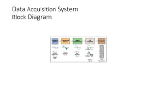
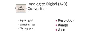
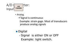
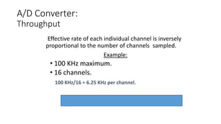
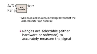
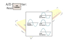
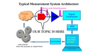
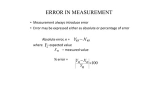
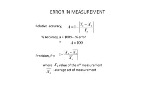
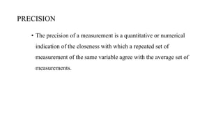
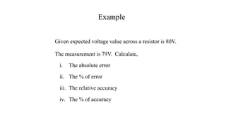
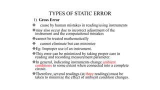
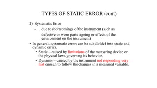
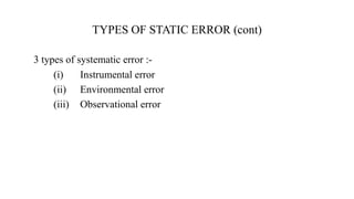
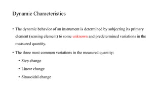
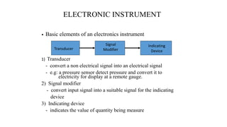
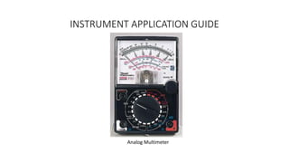
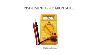
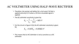
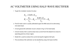
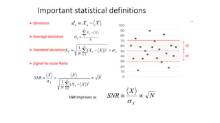
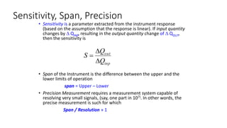
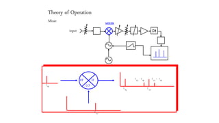
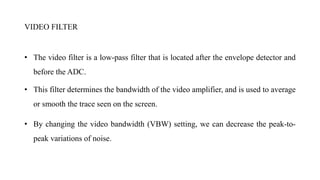
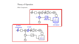
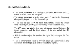
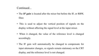
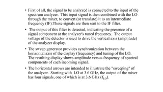
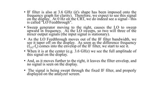
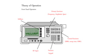
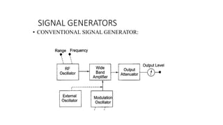
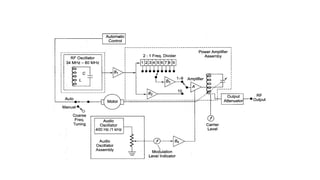
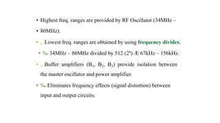
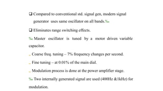
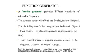
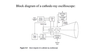
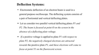
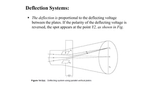
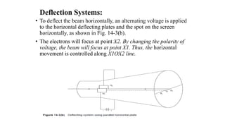
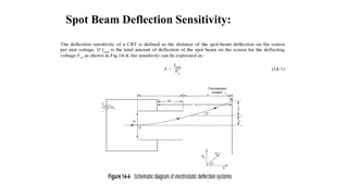
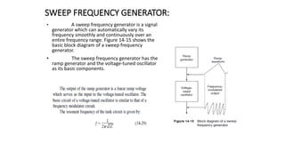
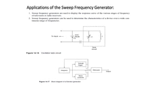
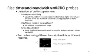
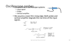
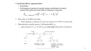
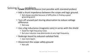
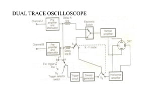
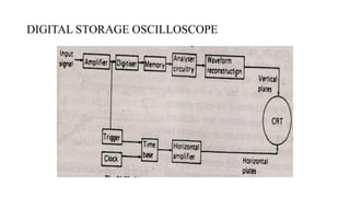
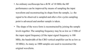
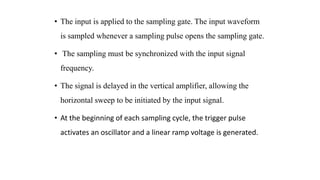
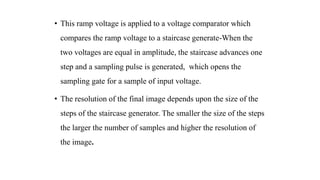
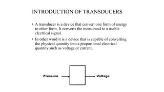
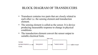
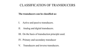
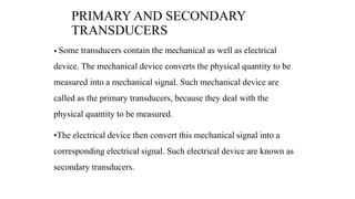
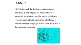
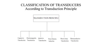
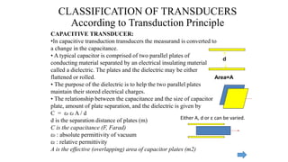
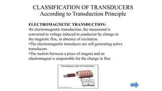
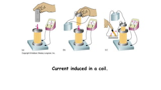
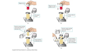
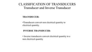
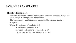
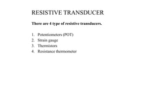
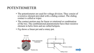
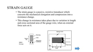
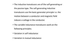
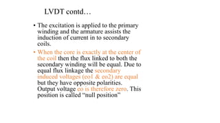
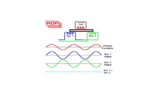
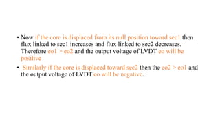
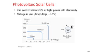
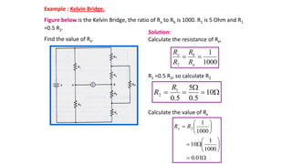
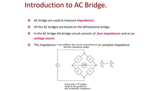
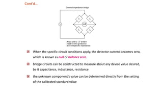
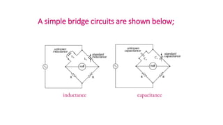
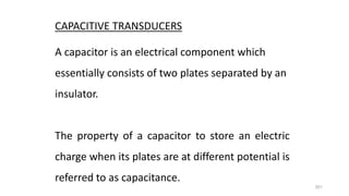
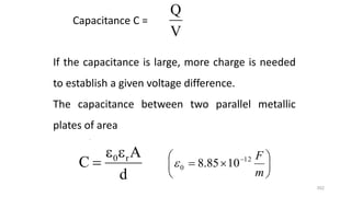
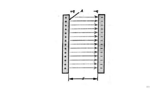
This document discusses electronic measurements and instrumentation. It begins with a typical block diagram of a measurement system including sensors, signal conditioners, analog-to-digital converters, and data storage. It then introduces instrumentation and defines measurement. Electronic instruments are based on electrical or electronic principles for measurement functions. The three basic functions of instrumentation are indicating, recording, and controlling. Electronic measurements provide advantages like high sensitivity and ability to monitor remote signals. Performance characteristics like accuracy, resolution, sensitivity allow selection of suitable instruments. Sources of error in measurement are also discussed.


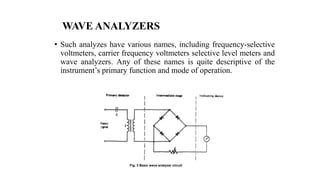
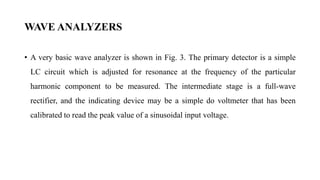


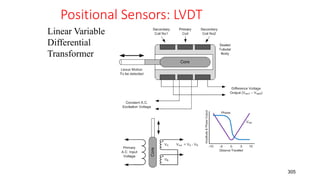


![360
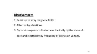
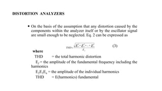
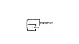
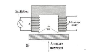
Advantages
1. Wide range of displacement from µm to cm.
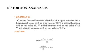
2. Frictionless and electrical isolation.
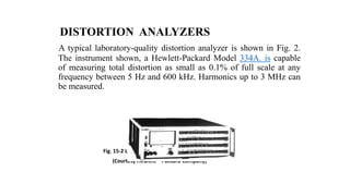
3. High output.
4. High sensitivity [sensitivity is expressed in mV (output
voltage)/ mm (input core displacement)].](https://image.slidesharecdn.com/emippt-240226101306-f86ebf61/85/Introduction-to-Emi-static-dynamic-measurements-360-320.jpg)