This thesis investigates the properties of iron depositions created using Electron Beam Induced Deposition (EBID). Two iron precursors, Fe3(CO)12 (TIDC) and Fe2(CO)9 (DINC), are characterized in terms of deposition yield, composition, and preliminary magnetic properties. An analytical model and computer simulation are developed to study the surface processes governing EBID, including adsorption, desorption, diffusion, and deposition. Experiments exploring the influence of substrate temperature, volatile contamination, and waiting time on deposition shape are performed and found to be in accordance with the developed model.


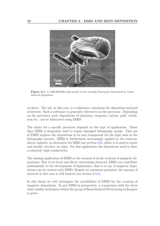
![2 CHAPTER 1. INTRODUCTION
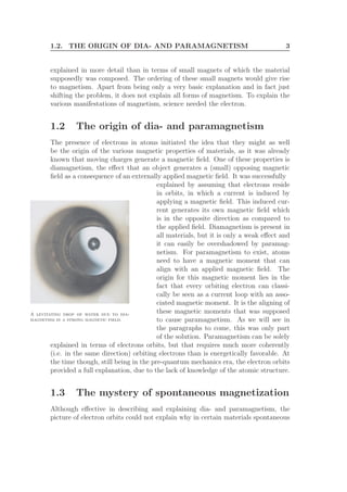
That the discovery of the electron changed the world as we knew it, is quite ap-
parent these days. The importance of the electron for our daily use lies not in its
mass, but in the charge that it carries. It is this charge that enables the enormous
scala of useful applications that we are so accustomed to today. Computers, mo-
bile phones, portable music players, but also the refrigerator and something as
natural as electrical lighting, it is hard to think of technical applications that do
not depend on electrons.
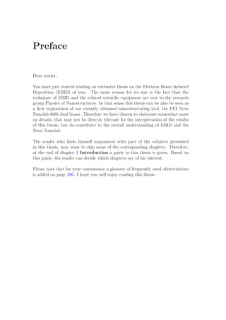
The discovery of the electron is mostly at-
Thomson experimenting in the Cavendish Lab-
oratory in Cambridge.
tributed to J.J. Thomson, who received a No-
bel price for his work on cathode rays in 1906.
Thomson found that these cathode rays con-
sisted of charged particles with a fixed mass
to charge ratio. The idea of a unit of charge
and the term electron itself were already in-
troduced in 1874 and 1894 respectively by G.
Johnstone Stoney, but it was Thomson who
is said to have identified it as a subatomic
particle. This was a revolutionary discovery,
because in those days it was believed that the
atom was the smallest indivisible entity that
the universe was build of, the ultimate build-
ing block. The Greek word £tomoj means uncuttable (i.e. something that cannot
be divided), hence the name atom.
Who actually can be said to have discovered the electron is still a point of con-
troversy as a few other physicians performed experiments similar to Thomson’s
experiments, even before him. In his contribution to the book Histories of the
Electron [1] Peter Archinstein sketches a extensive overview of all the different
contributions that lead to the discovery of the electron. As he argues, before
some conclusion can be drawn about who discovered the electron, it is necessary
to answer the philosophical question what it means to discover something. He
advocates that at least Thomson, more than any other, can legitimately be called
the discoverer of the electron. Besides Archinstein, 15 other authors contributed
to the book from their own perspective, which makes the story of the electron
very diverse and colorful and a must read for really everyone with an interest in
history, philosophy and applications of the electron.
The discovery of the electron enabled the explanation of a variety of phenom-
ena on a more fundamental level, one of which was magnetism. Magnetism due
to magnetic materials has been known to men since before the start of the Gre-
gorian calendar. The origin of this strange invisible force, however, had not been](https://image.slidesharecdn.com/f1d9af8f-520d-4711-b40c-d67fd4a14028-161106155501/85/Graduation-Thesis-TUe-Michael-Beljaars-10-320.jpg)
![4 CHAPTER 1. INTRODUCTION
magnetic ordering occurred below a certain critical temperature, an effect which
is known as ferromagnetism. The French physicist Pierre Ernest Weiss realized in
1906 that for a spontaneous magnetization to arise, there had to exist an internal
magnetic field that caused the magnetic moments to align. Weiss called this
internal field the molecular field. The description of magnetic materials in terms
of this field proved to be a very useful description of ferromagnetism, but what
gave rise to the Weiss molecular field remained unclear until the discovery of a
new property of the electron, the electron spin.
1.4 Give it a spin
With the identification of the electron as a carrier of quantized charge the explo-
ration had only just begun. Additional qualities of the electron were discovered,
like the pairing of electrons in so called Cooper pairs, the underlying mechanism
for superconductivity.
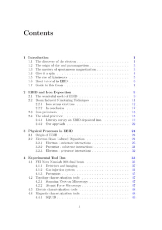
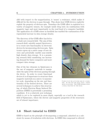
In 1925 Samuel Goudsmit en George Uhlen-
(l-r) Samuel Abraham Goudsmit, Hendrik
Kramers and George Eugene Uhlenbeck
around 1928 in Ann Arbor.
beck, both students of Paul Ehrenfest in Lei-
den, daringly posed an extra property of the
electron [2]. Besides a charge, they specu-
lated, an electron also should have a intrinsic
spin, an orbital moment. This spin gives the
electron a permanent magnetic moment.
It was a bold proposition, because how could
a supposedly point particle have spin, a prop-
erty that classically is associated with the ro-
tation of a body around its own axis? For
that reason the scientific community remained
sceptical to say the least, especially because
the paper of Goudsmit and Uhlenbeck lacked
a formal derivation. If they would have formally derived the formula for the
Land´e g-factor, the factor that relates orbital momentum to its corresponding
magnetic moment, they would have found that there was a factor of 2 missing,
as was remarked by Heisenberg in response on their article. Luckily this had
not withdrawn Goudsmit and Uhlenbeck from publishing as not much later a
young physicist Llewellyn H. Thomas in Copenhagen came up with a relativistic
derivation of the g-factor in which the factor of 2 popped up [3]1
.
1
If you are fascinated by the story of the discovery of the electron, you may find it interesting
to know that there is a document available on the internet in which Goudsmit describes his
personal view on the discovery of the electron spin. The document is a translation of the closing
lecture Goudsmit gave during the golden jubilee of the Dutch Physical Society in 1971[4].](https://image.slidesharecdn.com/f1d9af8f-520d-4711-b40c-d67fd4a14028-161106155501/85/Graduation-Thesis-TUe-Michael-Beljaars-12-320.jpg)
![1.5. THE RISE OF SPINTRONICS 5
The introduction of spin changed the theoretical picture behind paramagnetism
quite significantly. It was realized that for some materials not so much the orbital
magnetic moment contributed to this effect, but that it was the electron spin and
its associated magnetic moment that to a greater extent caused the uncompen-
sated net magnetic moment.2
Within the framework of the upcoming quantum
Visualization of the wavefunction of an
electron. Picture taken from [5].
mechanics, it was Heisenberg3
who proved that be-
cause of the property of spin, electrons interact,
besides the known electrostatic repulsion, via a so-
called exchange mechanism. This exchange mecha-
nism gives rise to an additional energy contribution
for the electron orbits and makes it favorable for
spins to couple either parallel or anti-parallel, de-
pending on the sign of the exchange integral. The
former case leads to ferromagnetism, whereas the
latter is the cause for antiferromagnetism. Anti-
ferromagnetic materials produce no external mag-
netic stray field, due to the internal compensation
of the spins.
So there you have it: we found the electron and ‘gave’ it a spin. This lead
to a lot of new insights with respect to the atomic structure and the origin of
magnetism. For almost a century the electron and its spin remained an interest-
ing study object, but it was not realized until the end of the 20th century that
spin transport could be of vital importance in a direct application.
1.5 The rise of Spintronics
In 1988 Peter Gr¨unberg and Albert Fert discovered the Giant Magneto Resistance
(GMR) effect, for which they received the Nobel price in 2007. The GMR effect is
based on the resistance of a nonmagnetic metallic spacer sandwiched between two
ferromagnetic layers. The device is constructed as such that the magnetizations
of the ferromagnetic layers are oriented either parallel or antiparallel. In parallel
configuration the device has a low electrical resistance, while in the anti-parallel
configuration it has a high resistance.
The underlying cause for this effect is related to the fact that electrons have
spin. Recalling that spin is nothing but a small magnetic moment, it can be
expected to interact with a magnetic field. It turns out that when this spin
is aligned parallel with the magnetization of the materials it travels through, it
fairly easily ‘floats’ through. On the other hand, when the spin is aligned antipar-
2
This great influence arises from the difference in g-factor, which in case of orbital momentum
is equal to 1, whereas for spin momentum equals 2. This means that for similar orbital and
spin momentum, spin momentum accounts for 2/3 of the magnetic moment of the atom.
3
A interesting overview of Heisenberg’s contributions to the understanding of ferromag-
netism is given in a paper by Sabyasachi Chatterjee[6].](https://image.slidesharecdn.com/f1d9af8f-520d-4711-b40c-d67fd4a14028-161106155501/85/Graduation-Thesis-TUe-Michael-Beljaars-13-320.jpg)
![1.7. GUIDE TO THIS THESIS 7
to as the precursor. The precursor containing the element(s) of interest is brought
in gas phase at a substrate, on which it partially adsorbs. Subsequently the ad-
sorbed precursor molecules are locally decomposed by irradiation with electrons.
After decomposition the fractions of the former precursor molecules either pre-
cipitate on the substrate (in the case of non-volatile ‘heavy’ fractions) or leave
the substrate altogether (in the case of volatile ‘light’ fractions). It are these
settling fractions that form the deposition referred to in the name Electron Beam
Induced Deposition. Ideally these fractions only consist of the desired material,
but reality learns us that this is mostly not the case. Due their presence in the
precursor and in hydrocarbons present in the system, part of the deposition will
consist out of carbon atoms. Obtaining a high purity in EBID depositions is still
one of the challenges to be faced, although recent studies have shown purities up
to 95 atomic percent [7].
1.7 Guide to this thesis
In this thesis we will explore the application of Electron Beam Induced Deposition
in Spintronics. Specifically we will be focussing on the creation of depositions of
magnetic materials and investigate their shape, composition and magnetic prop-
erties. For this purpose the ferromagnetic transition metal iron is chosen as a
model system. We will show, using a computer simulation, that specific shapes
of depositions are caused by surface processes such as diffusion. Furthermore, we
will see that the composition of EBID depositions highly depends on the choice
of precursor and on the deposition environment. Last, but most certainly not
least we will demonstrate the ferromagnetic properties of the depositions.
This last section is a quick guide to this thesis to provide the reader with an
overview of the chapters and how these relate to each other. To obtain a con-
densed overview of this research, it is suggested to start reading at chapter 5.
Note however that for a thorough understanding of the results, knowledge of the
other chapters may be useful.
In this chapter Introduction a general motivation for this type of research was
given. In the first part of chapter 2 EBID and Spintronics a more detailed
motivation for the choice of EBID is given. In the second part an overview of
publications on the subject of EBID deposited iron is given, after which our spe-
cific approach is motivated
Chapter 3 Physical Processes in EBID starts with a brief exploration of
the history of EBID and continues with an extensive explanation of the theory
behind this technique. Some special attention goes to the physics of electron -](https://image.slidesharecdn.com/f1d9af8f-520d-4711-b40c-d67fd4a14028-161106155501/85/Graduation-Thesis-TUe-Michael-Beljaars-15-320.jpg)
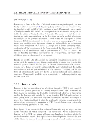
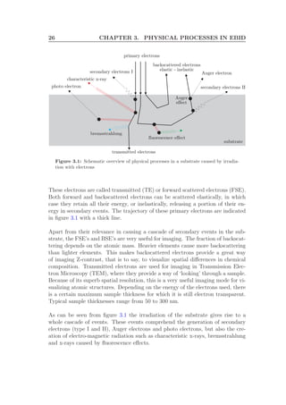
![14 CHAPTER 2. EBID AND IRON DEPOSITION
SRIM (Stopping Range Ions in Matter) is used [8]. The interaction of electrons
with the silicon substrate is simulated with a Monte Carlo based program called
Casino [9].
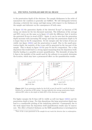
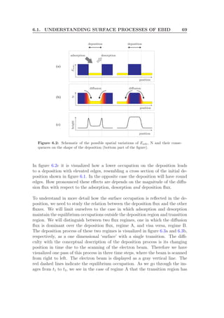
depth (nm)
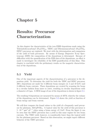
dissipatedenergy(a.u.)
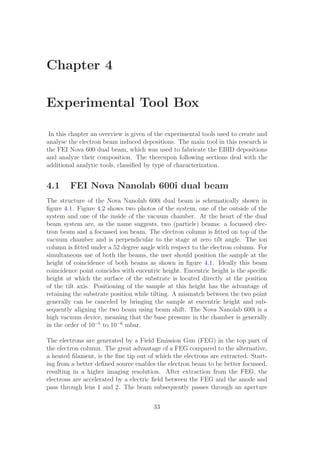
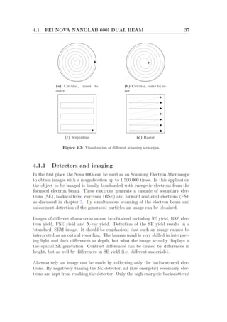
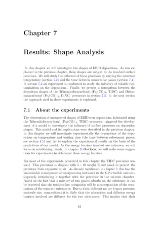
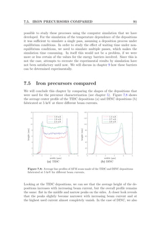
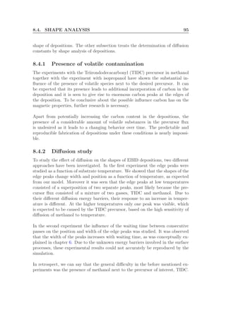
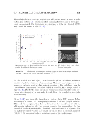
Figure 2.3: Comparison of the depth distribution of dissipated energy between 2 and
30 keV electrons and 30 keV Gallium ions in a Si substrate. The inset shows a zoom in
of the two electron graphs, where 2 keV corresponds to the right axis and 30 keV to the
left axis as indicated by the arrows. It can be seen that ions dispose much more energy
close to the surface than electrons, causing a more efficient decomposition. The integral
of the curves is related to the total dissipated energy. Data is generated with Casino (for
the electrons) and SRIM (for the ions).
As can be seen from figure 2.3, the energy dissipated by the 30 keV ion is more
concentrated near the surface than the energy of the 30 keV electron. It can be
expected that the amount of decomposition is correlated with the energy density
at the surface of the substrate. The energy density at the surface depends on the
local dissipated energy as well as on the transport of dissipated energy deeper
in the substrate towards the surface by secondary mechanisms. This means that
the energy distribution displayed in figure 2.3 has to be integrated, taking into
account a depth dependent scaling factor to obtain the total energy density at](https://image.slidesharecdn.com/f1d9af8f-520d-4711-b40c-d67fd4a14028-161106155501/85/Graduation-Thesis-TUe-Michael-Beljaars-22-320.jpg)
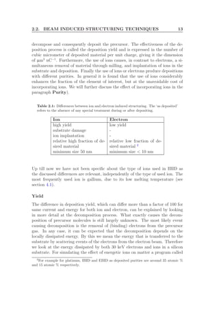
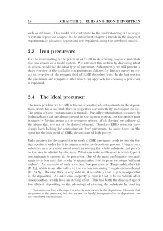
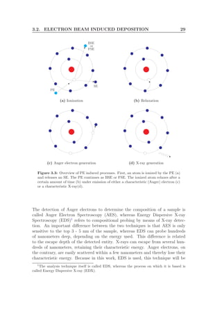
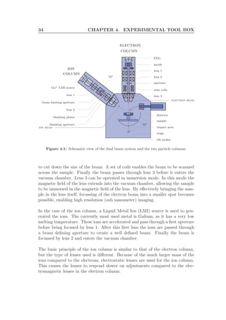
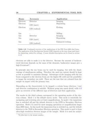
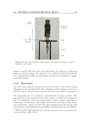
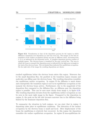
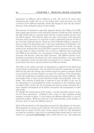
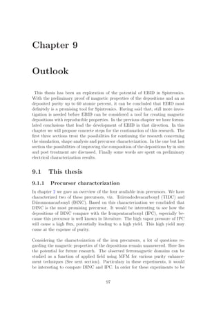
![16 CHAPTER 2. EBID AND IRON DEPOSITION
deposition area
depositiondiffusion edge
(a)
substrate
visualized flux
GIS needle
(b)
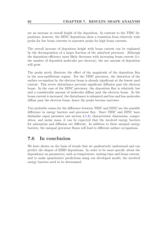
Figure 2.4: Scanning Electron Microscope (SEM) image of a deposition made with
IBID, using a 30 keV 9.3nA Ga focussed ion beam. Figures (a) and (b) show the same
SEM image, but for clarity in (b) a drawing of the needle and a visualization of the flux
are added (not to scale).
Ion implantation
The most important disadvantage of using ions, especially in the application of
structuring magnetic materials, is the unavoidable implantation of Ga ions. First
of all, the use of ions adds an extra contaminant to the depositions. Secondly,
it is know from literature that the implantation of Ga ions affects the magnetic
properties of materials. In [10] it is reported that implantation leads to a decrease
of the GMR effect and exchange bias field. On the other hand it has been shown
that properties such as the coercive field can be enhanced by Ga implantation
[11]. It must be noted that the situation in these papers is not directly similar to
the implantation of ions in IBID, but it can be expected that the ions will have
an effect. If this effect is significant in IBID deposited magnetic materials is still
something that has to be researched.
Purity
The main advantage of using ions with respect to electrons is the higher purity
of the depositions. The current hypothesis is that this effect is caused by a more
complete decomposition (i.e. breaking of the precursor into smaller fractions)
due to the much higher energy density and release of ions and neutrals from the
substrate. A higher purity in general leads to better qualities such as a larger
conductivity in case of metals and a larger magnetization in case of ferromag-
netic materials. However, it could be that the positive effect of the purity on the
magnetization is counteracted by the implantation of Ga ions in the case of IBID](https://image.slidesharecdn.com/f1d9af8f-520d-4711-b40c-d67fd4a14028-161106155501/85/Graduation-Thesis-TUe-Michael-Beljaars-24-320.jpg)
![2.4. THE IDEAL PRECURSOR 19
with other contaminants.
Although for various materials carbon free precursors have been found or de-
veloped, no such precursor exists for the deposition of iron today. One could
think of synthesizing a custom developed precursor for this purpose, but that is
a project of its own. Therefore we will focus on the existing precursors.
2.4.1 Literary survey on EBID deposited iron
Iron precursors
Table 2.2 gives an overview of the four currently known iron precursors in lit-
erature. These precursors originate from a technique called Chemical Vapor
Deposition (CVD), in which a molecule is thermally decomposed on a substrate.
Three of the four precursors belong to the same chemical category, i.e. the car-
bonyl group. By photolysis and heating Fe(CO)5 is transformed in Fe2(CO)9 and
Fe3(CO)12, respectively. The fourth precursor is commonly used in a non local
deposition process called Chemical Vapor Deposition (CVD), where the precur-
sor is decomposed due to a high substrate temperature.
Table 2.2: Overview of the currently known iron precursors.
Name Formula Atomic % Fe Weight % Fe
Iron-penta-carbonyl Fe(CO)5 9.1 28.5
Di-iron-nona-carbonyl Fe2(CO)9 10 30.7
Tri-iron-dodeca-carbonyl Fe3(CO)12 11.1 33.3
Ferrocene Fe(C5H5)2 4.8 30.0
(Iron-cyclo-penta-dienyl)
Although not new, the deposition of iron by means of EBID is relatively un-
explored. In table ?? an overview is given of which precursors were found in
literature. The process of EBID using Fe(CO)5 was first shown by Kunz [12],
although it is not indisputably shown that iron is deposited.
The possibilities of the deposition of iron using the Ironpentacarbonyl precur-
sor were studied extensively by a Japanese research group. They are one of the
few who published multiple papers on this subject, starting in 2004 with the
investigation of iron nanopillars and the effect of annealing on their shape and
composition [13]. In the paper it is shown that the as deposited pillars consist of
an amorphous mixture of Fe and C and are covered with an oxide layer. After](https://image.slidesharecdn.com/f1d9af8f-520d-4711-b40c-d67fd4a14028-161106155501/85/Graduation-Thesis-TUe-Michael-Beljaars-27-320.jpg)
![20 CHAPTER 2. EBID AND IRON DEPOSITION
Table 2.3: Overview of publications per iron precursor.
Precursor name Precursor formula Reference
Ironpentacarbonyl Fe(CO)5 [12, 13, 14, 15, 16, 17,
18, 19, 7]
Diironnonacarbonyl
Fe2(CO)9 -
Triirondodecacarbonyl
Fe3(CO)12 [20]
Ferrocene Fe(C5H5)2 [18]
annealing for 1 hour at 600◦
C the depositions had turned into a mixture of α-Fe
and several iron carbides.
Subsequent papers [14, 15] from the same group deal more extensively with the
magnetic properties, visualized and quantified by means of electron holography.
Next their focus is shifted to the crystallographic structure of the depositions and
the possibilities to enhance this [16, 17]. It is shown that the addition of water
vapor decreases the carbon content of the depositions at the expense of incorpo-
rating more oxygen. Above a certain ratio of iron precursor to water vapor flux,
polycrystalline Fe3O4 depositions can be obtained.
In a recent paper from Furuya et al a comparison of the magnetic properties
is made between depositions made with Ironpentacarbonyl and an alternative
iron precursor, Ferrocene (Fe(C5H5)2) [18]. By changing the relative fluxes depo-
sitions are created with varying Ferrocene to Ironpentacarbonyl content. These
depositions are then characterized by their remanent magnetic flux density, again
using electron holography. From these results it is concluded that, because a
higher Ferrocene content decreases the remanence, less iron is incorporated in
these depositions. From this it is concluded that the Ferrocene contributes less
iron atoms to the depositions compared to foreign atoms (carbon, oxygen) than
Ironpentacarbonyl.
In a paper by Bruk et al. [20] the electrical properties of Triirondodecacarbonyl
(Fe3(CO)12) depositions are investigated as function of beam current, deposition
time and temperature. It is shown that the resistance of the depositions decreases
with increasing beam current and deposition time. Preliminary experiments at
15 and 20 keV indicate an increase in the resistance with increasing electron beam
energy. The measurements of the resistance as function of temperature reveal a
positive temperature coefficient, pointing at non metallic conduction. The paper
is concluded with a preliminary experiment that shows the influence of the envi-
ronment of the depositions during measuring of the resistance. It is shown that](https://image.slidesharecdn.com/f1d9af8f-520d-4711-b40c-d67fd4a14028-161106155501/85/Graduation-Thesis-TUe-Michael-Beljaars-28-320.jpg)
![2.4. THE IDEAL PRECURSOR 21
the addition of water vapor has a permanent effect on the resistance, whereas the
addition of acetone and ammonia only reduce the resistance while present in the
system. Regrettably no magnetic characterization is performed.
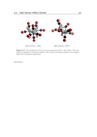
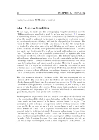
600 nm
Figure 2.5: Reconstructed phase image of an electron holographic image of a magnetic
bar deposited at the end of a tungsten tip. Adapted from [19].
Applications of EBID deposited iron
To conclude this section, two papers showing the application of iron EBID de-
positions are discussed. One of these papers is from the Japanese group [19] and
shows the growth of a nanomagnet (see figure 2.5) on top op a tungsten tip. By
approaching magnetic nanostructures on a substrate with this tip, the magnetic
interaction between the two can be studied. This technique is very similar to
Magnetic Force Microscopy (see chapter 4), where a magnetically coated tip is
used. One can think of using EBID to coat a tip with magnetic material using
EBID rather than to grow a nanomagnet, to approach or supersede the spatial
resolution of MFM. An alternative approach may be the perpendicular growth
(in contrast to the lateral growth of the nanomagnet shown in figure 2.5) of a
magnetic pillar on the end of a tip.
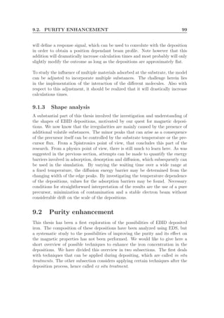
In the other paper, by M¨uller et al [21], it is shown that the resistance of a
Permalloy strip is influenced by the magnetic configuration of an EBID deposited
array of iron nanopillars (see figure 2.6). This effect is caused by the change in
magnetoresistance of the Permalloy strip due to the magnetic coupling with the
array. This application already shows the potential of EBID in Spintronics.](https://image.slidesharecdn.com/f1d9af8f-520d-4711-b40c-d67fd4a14028-161106155501/85/Graduation-Thesis-TUe-Michael-Beljaars-29-320.jpg)
![22 CHAPTER 2. EBID AND IRON DEPOSITION
Figure 2.6: SEM images (left) and schematic (right) of an array of iron EBID deposi-
tions on a permalloy strip. Adapted from [21].
2.4.2 Our approach
A first approximation of the final composition of the depositions is the atomic
iron fraction in the precursors. Based on this approximation, Ferrocene is not
expected to lead to the highest iron content. Therefore the focus of this thesis
will be on the precursors in the iron carbonyl group.
Considering the carbonyls, most experimental data is available on the Ironpen-
tacarbonyl, therefore using this precursor would give the research a head start.
However, one disadvantage of Ironpentacarbonyl is its toxicity. Therefore we
have chosen to start with characterizing the depositions of Triirondodecacar-
bonyl (TIDC) and work our way via the Diirondodecacarbonyl (DINC) to the
Ironpentacarbonyl (IPC).
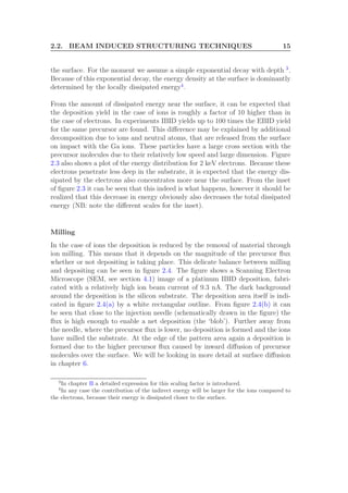
Within the time frame of this research only the first two mentioned precursors
have been used. 3D views of these precursors are shown in figure 2.7. One of
the aspects of the used supply of TIDC precursor is that it is shipped in a 5 - 10
weight % methanol solution to protect it from exposure to air. We need to be
aware that if this methanol is introduced in the vacuum chamber together with
TIDC, this may have consequences for our depositions. The DINC precursor is
shipped under argon atmosphere, which is not expected to be of great influence
due to its inert nature.
Both the TIDC and DINC are characterized by deposition yield, composition
and magnetic properties of the depositions in chapter 5. The origin of partic-
ular shapes of the depositions, as briefly introduced in the introduction, was
first spotted using the TIDC precursors. Therefore the further investigation of
these shapes in chapter 7 is based on the depositions created with this precursor.
Nonetheless the outcome of this investigation will be applicable to many other](https://image.slidesharecdn.com/f1d9af8f-520d-4711-b40c-d67fd4a14028-161106155501/85/Graduation-Thesis-TUe-Michael-Beljaars-30-320.jpg)
![Chapter 3
Physical Processes in EBID
As introduced and motivated in the previous chapter, the main subject of this
thesis is Electron Beam Induced Deposition (EBID) of the ferromagnetic tran-
sition metals iron. In this chapter we will elaborate more on the origin and
qualitative description of EBID. A qualitative description of EBID. A real quan-
titative description is postponed until chapter 6.
3.1 Origin of EBID
The development of beam induced structuring techniques started with the discov-
ery of EBID. Beam Induced Deposition was discovered as an undesired side effect
of Scanning Electron Microscopes (SEM) [22]. It was found that while scanning
with SEMs carbon was deposited on the substrate. This carbon deposition was a
consequence of adsorbed organic molecules decomposing under irradiation with
the electron beam.
At first this contamination deposition was seen as a nuisance, an annoying conse-
quence of the use of oil diffusion pumps, O-rings and grease, until in 1976 Broers
came up with the idea to use the carbon deposition as a negative resist during
reactive ion etching. He proved it to be possible to produce 80 ˚A thin metal lines
with this new technique called contamination lithography [23]. Since Broers dis-
covery various variations of beam induced processes have been developed, which
we already introduced in the previous chapter as Beam Induced Structuring tech-
niques.
3.2 Electron Beam Induced Deposition
Although the principle behind EBID is relatively simple, the exact processes un-
derlying this technique are numerous and complex. The aim of this chapter is to
give the reader insight in some of the processes that are relevant to this research.
It is beyond the scope of this thesis to present a full overview of what is known
about EBID. The interested reader can find an overview of EBID in the review
24](https://image.slidesharecdn.com/f1d9af8f-520d-4711-b40c-d67fd4a14028-161106155501/85/Graduation-Thesis-TUe-Michael-Beljaars-32-320.jpg)
![3.2. ELECTRON BEAM INDUCED DEPOSITION 25
article by S.J. Randolph et al [24]. Furthermore an extensive work on EBID,
including a valuable literature study, was performed by Silvis-Cividjian [25]. A
more recent work that focusses on simulating EBID can be found in the thesis of
Smith [26].
For simplicity and because of its origin, EBID was introduced as a deposition
process by means of a focussed electron beam. In principle any electron source is
capable of inducing decomposition, provided that the electron energy exceeds a
certain threshold. This threshold is easily reached by many electron sources, since
it is related to the chemical bond strength, which generally is not higher than 10 to
20 electron volts. Apart from the most frequently used Scanning Electron Micro-
scope (SEM) as a tool for EBID, also Transmission Electron Microscopes (TEM),
Scanning Transmission Electron Microscopes (STEM) and Scanning Tunneling
Microscopes (STM) are used. In this thesis we will focus on SEM and conse-
quently the relevant equipment for SEM will be dealt with more extensively in
this thesis. For specific applications one of the other tools might have advantages
over the others. For more information on these techniques we refer to [25].
As outlined in chapter 2, EBID can be seen as an interaction between three
subsystems, which are the electron (beam), the precursor and the substrate. We
will now discuss the interactions between these subsystems. It should be empha-
sized that once a precursor molecule is adsorbed on the substrate, it is considered
to be part of the substrate. This means that interactions of the electrons with
the adsorbed precursor are mediated via the substrate. It does not mean however
that these molecules are considered to be stuck on the substrate, as if they where
already deposited.
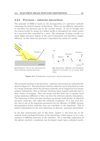
3.2.1 Electron - substrate interactions
Depending on its energy, several physical processes can occur when a electron
hits a substrate. Figure 3.1 displays a schematic overview of these processes. Not
all of these processes are relevant for EBID, but because some of these processes
are of importance for Energy Dispersive X-ray Spectroscopy (see chapter 4), we
will present the full picture here. At the end of this subsection, a short summary
is given to clearly recapitulate the important processes.
Considering the case of a primary electron (PE) hitting the substrate, there are
three possible futures. Either it leaves at the same side it entered the substrate,
in which case it is called a backscattered electron (BSE). It can be stopped inside
the substrate after releasing all its energy in secondary events. Or, in the case
the substrate is thin enough with respect to the energy of the electron, it is trans-
mitted and leaves the substrate on the other side, generally with a lower energy.](https://image.slidesharecdn.com/f1d9af8f-520d-4711-b40c-d67fd4a14028-161106155501/85/Graduation-Thesis-TUe-Michael-Beljaars-33-320.jpg)
![3.2. ELECTRON BEAM INDUCED DEPOSITION 27
Secondary electrons
Secondary electrons (SE) are electrons that originate from the ionization of atoms
due to irradiation with the PE’s and subsequent BSE’s and FSE’s. They have a
non-specific energy which can be anywhere between zero and the energy of the
PE’s. Figure 3.3(a) schematically shows the ionization process for an atom with
10 electrons (i.e. Neon).
Strictly speaking, one can discriminate between SE of type I and type II. SE
I’s are electrons that are generated by ionization due to the PE’s, whereas SE
II’s are generated by the BSE’s and FSE’s. This mainly expresses itself in differ-
ence in the radial distance from where the PE’s strike the substrate. SE II’s are
more likely to be generated further from the point of incidence of the PE beam
as compared to the SE I’s.
The generation of SE’s is exploited in Scanning Electron Microscopy, where the
spatial dependent intensity of the SE’s is used to form an image. How this tech-
nique exactly works, is described in more detail in chapter 4. Considering EBID,
the SE’s are the main cause for the decomposition of the adsorbed precursor
molecules due to their relative low energy and consequently larger cross section
with the precursor. Therefore the deposition yield depends highly on the SE yield
in the substrate. An empirical formula that successfully describes the SE yield
for a variety of materials as function of energy is
δ
δm
= 1.28 ∗
EP E
EM
P E
0.67
1 − exp −1.614
EP E
EM
P E
[27] (3.1)
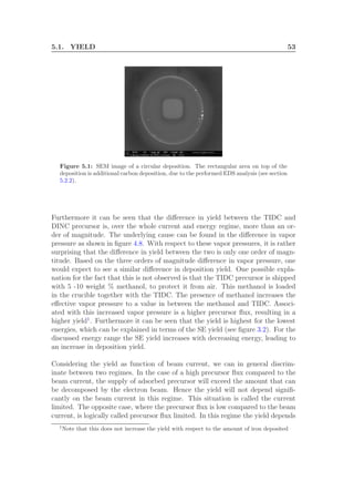
This formula relates the ratio of the SE yield δ and its maximum δM to the ratio
of the used PE energy EP E and the PE energy of maximum SE yield EM
P E. Values
for δM and EM
P E are material dependent. A list of values for these parameters for
different materials can be found in [27]. In figure 3.2 equation 3.1 is plotted for
average values of δM and EM
P E, indicated by the solid line. The four dashed lines
show the SE curves for the extreme values of δM and EM
P E. From these extremes
we can indicate an area of maximum SE yield, marked by the hatched rectangle.
It can be seen that the maximum SE yield generally lies between 200 and 700 eV
and takes values from 0.25 up to 2 SE electrons per PE electron. Since we expect
the EBID deposition yield to be correlated with the SE’s, the highest EBID yield
is likely to be achieved at this energy.](https://image.slidesharecdn.com/f1d9af8f-520d-4711-b40c-d67fd4a14028-161106155501/85/Graduation-Thesis-TUe-Michael-Beljaars-35-320.jpg)
![28 CHAPTER 3. PHYSICAL PROCESSES IN EBID
0 1 2 3 4 5
0.0
0.5
1.0
1.5
2.0
2.5
PE energy (keV)
SEyield(SE/PE)
SE boundary curves
Typical SE curve
area of maximum
SE yield
Figure 3.2: A typical shape of the SE yield versus PE energy. The solid line shows
a typical SE yield versus PE energy curve. The dashed lines are plots of equation 3.1,
using extreme values for δM and EM
P E as given in [27]. The rectangle indicates the region
in which the maximum yield lies for most materials.
Auger electrons and X-rays
After ionization the atom eventually relaxes to a lower energy state. Figure
3.3(b) to 3.3(d) give a schematic overview of this process. The relaxation occurs
by transferring an electron from a higher shell to a vacant state in a lower shell.
As a consequence of this process a characteristic amount of energy is released, cor-
responding to the energy difference of the two states. This energy can be released
either through a solid state excitation, the emission of a characteristic X-ray or
by ejecting an electron out of one of the outer shells of the atom. This electron is
called an Auger electron, after its discoverer Pierre Victor Auger. Although solid
state excitations, or phonons, can give rise to an additional SE generation, they
are not discussed here. The energy carried by the phonons is very low compared
to the PE, BSE and FSE and thereby cause only a minor fraction of the total of
generated SE’s.
The generation of an electron or photon by relaxation of an atom to a lower
energy state are visualized respectively in figure 3.3(c) and 3.3(d). The energy
states in an atom have very well defined energies, which are different for every
element. Consequently the energy carried by the electron or photon is specific
for the transition and element in question. Therefore these emitted photons or
electrons can be used to determine the chemical composition of a sample.](https://image.slidesharecdn.com/f1d9af8f-520d-4711-b40c-d67fd4a14028-161106155501/85/Graduation-Thesis-TUe-Michael-Beljaars-36-320.jpg)
![32 CHAPTER 3. PHYSICAL PROCESSES IN EBID
Both the model and the simulation are dealt with in chapter 6.
3.2.3 Electron - precursor interactions
It has been shown that the interaction of free precursor molecules (i.e. not ad-
sorbed) and the electrons (PE, BSE and SE) does not contribute to the deposition
[12]. To put it differently, apparently only adsorbed molecules are efficiently de-
composed and form a deposition. There are different views that support this
result. Most importantly the density of the molecules in the chamber (even near
the needle) is in general much lower than the density on the substrate. The sub-
strate can in this case be seen as a reservoir for the precursor species. Secondly,
free fractions of decomposed molecules do not necessarily stick to the substrate
on the target position, or to the substrate at all. These two conditions justify
the assumption that direct decomposition of free molecules by primary electrons
can be neglected and that only adsorbed molecules have to be taken into account.
The adsorbed molecules are subjected to a shower of PE’s and SE’s, as explained
in subsection 3.2.1. How this exactly leads to decomposition of the molecule is
still largely unknown. In this thesis it is assumed that the SE’s are the main cause
for decomposition, based on the large cross section with the molecules compared
to the PE’s.](https://image.slidesharecdn.com/f1d9af8f-520d-4711-b40c-d67fd4a14028-161106155501/85/Graduation-Thesis-TUe-Michael-Beljaars-40-320.jpg)
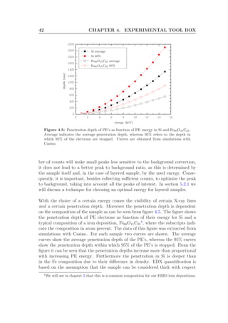
![40 CHAPTER 4. EXPERIMENTAL TOOL BOX
energy (keV)
counts
L lines
K lines
bremsstrahlung
bremsstrahlung
Figure 4.4: Spectrum of iron, collected using 15 keV electrons. The K and L series are
indicated with a rectangular marker. Also the continuum X-ray radiation, the so called
Bremsstrahlung, can be seen.
ference between these two states is very well defined and characteristic for the
atom in question. This energy is either used to free an electron, which is called
an Auger electron or emitted as a X-ray. The EDX detector detects the incom-
ing x-rays and constructs a histogram of the amount of x-rays per energy range.
Typically this energy range (detector resolution) is in the order of 10 eV. The
histogram is called a spectrum and is unique for each element.
In figure 4.4 the spectrum of iron is shown. The appearance of peaks at defi-
nite positions in the energy spectrum makes it possible to identify the presence
of certain elements, in this case iron. These peaks are generally referred to as
X-ray lines and appear in series, labeled as K, L, M etc. corresponding to the
transitions between different shells [28]. In figure 4.4 both the K and L lines
of iron are shown. Each line series in principle consists of sub lines, labeled α,
β, γ etc., but in general only the α sub lines are visible due to their high tran-
sition probability. Consequently we refer to these lines as the K and L lines,
which technically means Kα and Lα respectively. In most cases, however, one
is interested not only in the possible presence of an element, but merely in its
relative abundance. The process of determining relative abundances is called
quantification.](https://image.slidesharecdn.com/f1d9af8f-520d-4711-b40c-d67fd4a14028-161106155501/85/Graduation-Thesis-TUe-Michael-Beljaars-48-320.jpg)
![4.1. FEI NOVA NANOLAB 600I DUAL BEAM 41
Quantification The identification of elements is relatively simple compared
to the quantification of elements. Quantification is based upon the so called k-
ratios, the ratio between the measured peak intensity and the peak intensity of
a reference spectrum of that same element. In the case this reference spectrum
is a spectrum of the pure element or a compound with known composition, it
is called a standard. By multiplication with correction factors for atomic mass
(Z), absorption (A) and fluorescence (F) these k-ratios are linked to a weight
percentage3
.
The EDAX software package that controls the EDX is called Genesis and pro-
vides two ways to perform quantification. The first method is through the use
of the before mentioned standards. To obtain reliable results, all the standard
spectra of the element of interest should be collected under the same conditions
as the spectra of the sample to be analyzed. Same conditions refer to same beam
energy, beam current, sample position and orientation. Preferably the collection
of the spectra of the sample and standards are performed directly after each other.
The second method for quantification is called standardless and as the name sug-
gests this method enables quantification without the use of physical standards.
To obtain a reference spectrum for calculating k-ratios, standardless quantifica-
tion uses a model of the X-ray generation in a sample. The great advantage of this
method is the absence of requiring standards. The collection of standard spectra
can be a time consuming procedure, depending on the amount of elements to be
quantified. On the other hand the use of standards can lead to a more accurate
quantification, especially at low energy.
For both quantification methods, it is important to correct for the non element
specific Bremsstrahlung (see section 3.2.1). This is done by curve fitting through
points that are expected to have no element specific counts. It should be realized
that especially for low count peaks, the inaccuracy in the background correction
can alter the outcome of the quantification. This situation is common for spectra
in which one peak dominates the other peaks. In this case we say that the low
count peaks are masked by the high count peak.
Related to this masking issue, are the statistics involved in the collection of a
spectrum. Because the error in this type of measurement scales with the square
root of the number of counts, a considerable number of counts are needed in
order to obtain a spectrum reliable for quantification. The number of counts can
be increased by using a higher electron beam current, decreasing the detector -
sample distance or measuring for a longer time. Although increasing the num-
3
Alternative correction methods are sometimes used depending on the application. See
chapter 9 of [28] for more information.](https://image.slidesharecdn.com/f1d9af8f-520d-4711-b40c-d67fd4a14028-161106155501/85/Graduation-Thesis-TUe-Michael-Beljaars-49-320.jpg)
![44 CHAPTER 4. EXPERIMENTAL TOOL BOX
chapter 5.
In theory it is possible to perform quantifications with an accuracy up to 0.1
atom percent. In practice this can be hard to achieve. Problems arise when
peaks of different elements overlap or when quantities are small. The aim of the
EDX quantification in this thesis is to obtain reliable reproducible results within
a few percent.
This section only provides a condensed view on EDX and EDX quantification.
For a more in depth exploration of X-ray generation and detection we refer to
[28].
4.1.2 Gas injection system
In chapter 3 we briefly mentioned two different ways to introduce a gas in the
vacuum system for the application of Beam Induced Structuring techniques, in
specific EBID. This either takes place by means of a valve controlled inlet (in-
jection throughout the whole vacuum system) or through a small hollow needle
(local injection). On the FEI Nova 600i dualbeam the gas is injected locally, close
to the substrate, by means of a hollow needle with an end diameter of 600 µm.
This needle is part of a larger system called the Gas Injection System (GIS). A
photo of a GIS is shown in figure 4.7.
The GIS consists of two major parts. The larger part is situated outside the
vacuum and contains a pneumatic system to insert and retract the needle and
to open and close the GIS. Inside the vacuum system the crucible is situated,
in which the precursor of choice is loaded. A plunger inside the middle of the
crucible acts as a valve and is operated by the pneumatics on the outside. The
crucible is equipped with a heater to bring the precursor to the desired temper-
ature. The temperature provides a way to control the precursor flux through
the needle. Heating of the precursor results in increased evaporation, thereby
increasing the flux through the needle.
The GIS is connected to the vacuum chamber of the Nova 600i by means of
a flange. This flange rests on a rubber O-ring that seals the vacuum chamber.
The unit is kept in place by two aluminium clamps in which the flange fits. By
means of little Allen screws in the clamps, pressure can be locally applied on
the flange. Because of the flexibility of the O-ring, this causes a slight change
in the alignment of the GIS. The length of insertion can be controlled through a
turnable ring, that acts as an stop. In this way the position and distance of the
needle with respect to the substrate and the two focussed beams can be adjusted.
The GIS should be aligned for operation at eucentric height. This ensures the](https://image.slidesharecdn.com/f1d9af8f-520d-4711-b40c-d67fd4a14028-161106155501/85/Graduation-Thesis-TUe-Michael-Beljaars-52-320.jpg)
![48 CHAPTER 4. EXPERIMENTAL TOOL BOX
Behind the simple principle on which AFM is based, hides a world of various
operating modes and force regimes. It is beyond the scope of this thesis to ex-
plain this in more detail. For a condensed overview of AFM, it is recommended
to read [29]. A more complete overview of the possibilities of this technique can
be found in [30].
4.3 Electric characterization tools
Electrical measurements were performed on depositions, situated between two
macroscopic golden electrodes as shown in figure 4.9(a). These electrodes were
fabricated using Electron Beam Litography (EBL) and lift-off technique. The
electrodes were contacted using four sharp needles (7 µm tip diameter), 2 needles
on each electrode. Two of the needles, one on each electrode, are used to send a
current through the deposition. The other two are used to measure the voltage
drop across the deposition. This type of conductivity measurement is generally
referred to as a four point measurement.
The positioning of the needles is done by means of a probe station. An optical
microscope is used to visually detect the landing of the needles on the electrodes.
An example view from the microscope is shown in figure 4.9(b). The picture
also shows a potential danger of this measuring technique. Due to electrostatic
charging of the needles, high potential differences can arise between the tip and
sample. When approaching the sample this potential difference results in a dis-
charge through the deposition, which causes partial evaporation of the deposition.
To avoid this destructive discharge, the needles should be temporarily grounded
before approaching the sample.
4.4 Magnetic characterization tools
For the magnetic characterization of the iron depositions, three different tools are
available within the group of Physics of Nanostructures. For quantitative mea-
surements there is the Superconducting QUantum Interference Device (SQUID).
Normalized measurements of the magnetization of samples can be preformed us-
ing the Magneto Optical Kerr Effect (MOKE). Finally there is Magnetic Force
Microscopy (MFM), which provides an accurate way of imaging the strayfield
emanating from the sample as a consequence of its local magnetization. These
three techniques are treated in the next sections.](https://image.slidesharecdn.com/f1d9af8f-520d-4711-b40c-d67fd4a14028-161106155501/85/Graduation-Thesis-TUe-Michael-Beljaars-56-320.jpg)
![4.4. MAGNETIC CHARACTERIZATION TOOLS 49
75 µm
(a) SEM image of the electrodes. In between
the thin ends the deposition is situated.
(b) Microscope image of the four needles on
the electrodes.
Figure 4.9: SEM image of the electrodes and microscope image of the electrodes and
needles.
4.4.1 SQUID
The full explanation of SQUID is beyond the scope of this thesis. A description
of SQUID can be found in [31]. For now it suffices to note that it is a relatively
sensitive technique to measure magnetic moments. In order to determine whether
SQUID is applicable in this research, we will estimate the minimum deposition
time necessary to obtain a measurable magnetic moment.
The sensitivity of the Superconducting Quantum Interference Device µmin avail-
able in the group is 10−9
A m2
. The volume necessary to obtain this magnetiza-
tion was estimated through
Vmin =
µmin
MF e
0
, (4.1)
using a value of 1.7 · 106
A m−1
for the saturation magnetization of pure iron
MF e
0 at 0 K7
. This leads to a volume of 6.0 · 102
µm3
of pure iron. After the
characterization of the deposition yield Y , an estimation is made of the deposition
time necessary to deposit this volume. Taking into account a 60 atomic percent
7
Because the Curie temperature for iron (1043 K) is high compared to room temperature
(300 K), the saturation magnetization at room temperature will not differ significantly from
the value at 0 K [32].](https://image.slidesharecdn.com/f1d9af8f-520d-4711-b40c-d67fd4a14028-161106155501/85/Graduation-Thesis-TUe-Michael-Beljaars-57-320.jpg)
![50 CHAPTER 4. EXPERIMENTAL TOOL BOX
iron concentration in the depositions8
(see section 5.2) leads to an estimate for
the effective iron deposition yield YF e in the order of 10−4
µm3
nC−1
for the TIDC
precursor. The time needed to create a deposition that can be detected in the
SQUID is given by
tdep =
Vmin
YF e · Iebeam
. (4.2)
Substituting the estimated values for the parameters gives a time of 6 · 105
s
for a typical electron beam current Iebeam of 1 nA. This is equivalent to almost
7 days, hence it is not considered practical to pursue the characterization of
the TIDC depositions using SQUID. Because of the considerable higher yield of
DINC, it may be feasible to determine the magnetic moment associated with the
depositions created with this precursor. This was not accomplished within the
time frame of this thesis, as we have focussed on the characterization of the TIDC
precursor.
4.4.2 MOKE
MOKE exploits the effect that the polarization of light is changed upon reflec-
tion on a magnetic sample due to interactions with the local magnetization. By
applying an external magnetic field to the sample and sweeping it from negative
to positive and back, a magnetic hysteresis curve can be obtained. The range
of the field sweep is dependent on the properties of the sample. From the hys-
teresis curve sample characteristics such as the coercive field can be determined.
Standard MOKE provides a normalized signal with respect to the saturation
magnetization, meaning that it does not provide an absolute value of the magne-
tization as function of applied field. The theory of MOKE is explained in more
detail in [31].
The main problem of the used MOKE setup with respect to the depositions
is the size of the laser spot. The spot is estimated to be 100 - 150 µm in diam-
eter, which is a factor of 100 more than the typical dimension of a deposition.
Consequently the MOKE signal will be small, if not impossible to detect. At-
tempts have been made to obtain MOKE hysteresis loops for small (5x5µm, 1h)
and large (100x100µm, 12h overnight deposition) samples, but none of them
were successful. An explanation for the lack of a MOKE signal in case of a small
deposition was already given at the beginning of this paragraph. In case of the
large deposition, the amount of magnetic material may have been too small to
measure or the deposition may lack a net magnetization due to domain formation.
8
It is hard to calculate the volume corresponding to 60 atomic percent iron due to unknown
densities of the other constituents. It can nevertheless be concluded that iron takes up no more
than 60 volume percent.](https://image.slidesharecdn.com/f1d9af8f-520d-4711-b40c-d67fd4a14028-161106155501/85/Graduation-Thesis-TUe-Michael-Beljaars-58-320.jpg)
![4.4. MAGNETIC CHARACTERIZATION TOOLS 51
MOKE is potentially a suitable tool to investigate the magnetic properties of the
depositions, provided that the spot size is optimized for analyzing micrometer
sized structures. Within the time frame of this thesis, this was not accomplished.
4.4.3 Magnetic Force Microscopy (MFM)
MFM can be seen as an extension of the capabilities of AFM. By replacing the
AFM tip with a magnetic MFM tip, the magnetic interaction of the tip with the
stray field of the sample can be studied. In order to distinguish between topology
and magnetic interactions, MFM uses a multi pass technique, meaning that every
scan line is scanned twice. In the first pass, the surface topology is determined,
while in the second pass a certain height above this topology is maintained during
scanning. The deflection of the cantilever in the second pass is a measure for the
magnetic interaction. A more detailed description of MFM can be found in [29].
The current shortcoming of MFM is the inability to quantify its signal due to
the unknown magnetic moment of the tip. The possibilities of the calibration
of a MFM tip were investigated in [33]. The results are promising, but further
research is required for the actual calibration. Consequently the MFM scans in
this thesis can only be interpreted qualitatively.
The measuring of magnetic stray fields with MFM is a very subtle process. The
success of MFM depends highly on the stability and reliability of the setup and
on the properties of the MFM tip. Especially for small stray field, such as ema-
nating from the iron EBID depositions, the interaction with the tip is only with
its mere end. Any small damage or pollution of the tip can result in total quench-
ing of the MFM signal. The used MFM is operated under ambient conditions,
which enables easy operation, but is also frequently accompanied with vibrational
noise and dust contamination. Especially because of the sensitivity of the MFM
technique these effect can be of great influence on the MFM signal.](https://image.slidesharecdn.com/f1d9af8f-520d-4711-b40c-d67fd4a14028-161106155501/85/Graduation-Thesis-TUe-Michael-Beljaars-59-320.jpg)
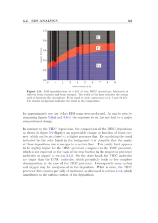
![5.2. EDS ANALYSIS 55
tion is generally unknown, which makes it hard to relate the decomposed fractions
to an experimentally determined yield. Due to these difficulties, a quantitative
description is an extensive task and beyond the scope of this thesis.
5.2 EDS analysis
The composition of the depositions is investigated using Energy Dispersive X-ray
Spectroscopy (EDS). EDS was developed for the analysis of homogeneous, mi-
cron scale bulk samples. Since we are dealing with nanometer thick depositions,
it should be investigated under which conditions EDS can still be used to analyze
these depositions.
An example of the difficulties that arise for EDS quantification of the iron depo-
sitions is given in table 5.1. EDS was performed using both 2 keV and 10 keV
electrons. The quantification was obtained using the Standardless quantification
of Genesis (see section 4.1.1). It can be seen that the quantification results differ
substantially. In the case of 2 keV an iron content of 61.8 atomic percent is found,
in contrast to the 16.0 atomic percent at 10 keV.
Table 5.1: EDS quantification of a iron deposition at 2 and 10keV.
Element Line Atomic %
2keV 10keV
C K 27.8 64.5
O K 10.4 19.5
Fe L 61.8 16.0
Total 100 100
As explained in section 4.1.1 this difference may be attributed to the difference
in penetration depth of the electrons. Where the 2keV electrons mainly generate
electrons within the deposition, the 10keV electrons largely probe the underlying
substrate. This large substrate signal masks the peaks of interest and increases
their sensitivity to the background correction. Based on this reasoning, the re-
sults obtained with 2keV electrons are expected to be more accurate.
Aided by a special software package for the EDS analysis of thin samples Stratagem
[34] an attempt is made to investigate quantification of thin samples. By study-
ing a Co90Fe10 layer of varying thickness, a so called wedge, we gain insight in
additional difficulties related to EDS quantification, which are not specifically
associated with thin films. Due to these difficulties, the found results can not
directly be related to the quantification of EBID iron depositions. However, we](https://image.slidesharecdn.com/f1d9af8f-520d-4711-b40c-d67fd4a14028-161106155501/85/Graduation-Thesis-TUe-Michael-Beljaars-63-320.jpg)
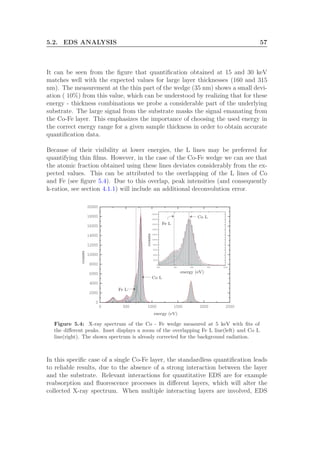
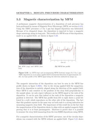
![58CHAPTER 5. RESULTS: PRECURSOR CHARACTERIZATION
quantification is not as straightforward. A possible solution to the difficulties
involved in EDS analysis on these samples is a software package called Stratagem
[34]. Stratagem can account for interactions between different layers and thereby
enables EDS quantification of layered samples. A bonus of Stratagem is its capa-
bility to determine the thickness of layers from the EDS data. The accuracy of
the results of Stratagem still depends on the reliability of the k-ratios determined
by Genesis. We will therefore focus on quantification with Stratagem using the
K-lines.
Additional EDS spectra are collected on the thin part of the wedge (0 - 140 nm)
using energies of 10 and 15 keV. The k-ratios of the K lines of these measure-
ments, returned by Genesis, are used in Stratagem to calculate the composition
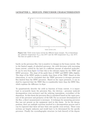
of the layer and the corresponding thickness. In figure 5.5 the results are shown.
0 20 40 60 80 100 120 140
0.0
0.1
0.2
0.8
0.9
1.0
thickness (nm)
atomicfraction
10 keV K
10 keV K
15 keV K
15 keV K
Co content
Fe content
(a) Composition in atomic percent as
function of layer thickness for 10 and 15
keV using the K lines.
0 10 20 30 40 50 60 70 80 90 100 110 120 130 140
0
20
40
60
80
100
120
140
160
actual thickness (nm)
Stratagemthickness(nm)
10 keV K
15 keV K
(b) Thickness as determined by
Stratagem versus actual thickness
Figure 5.5: Stratagem corrected quantification results and calculated layer thicknesses.
The quantification results obtained with the K lines agree with the expected val-
ues. The spectra collected at expected zero thickness reveal small Co K and Fe
K peaks, indicating that we are not exactly at the beginning of the wedge. The
deviation at this thickness is again a consequence of the masking of the Co K and
Fe K lines by the Si K line of the substrate. The negligible difference between the
results from Genesis and Stratagem confirms the absence of strong interactions
between the Co-Fe layer and the Si substrate.
Additional to the composition, Stratagem calculates the thickness of the layer.
Figure 5.5(b) shows the calculated thickness as function of the actual thickness of
the wedge. The thickness values returned by Stratagem match very well with the
expected thickness. The difference with the actual thickness may even be smaller](https://image.slidesharecdn.com/f1d9af8f-520d-4711-b40c-d67fd4a14028-161106155501/85/Graduation-Thesis-TUe-Michael-Beljaars-66-320.jpg)
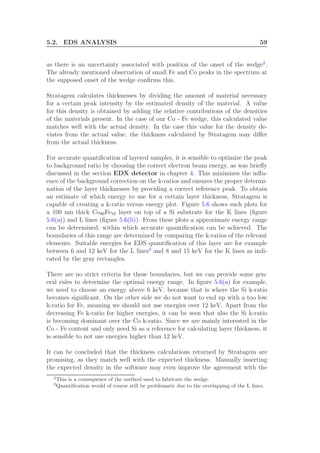
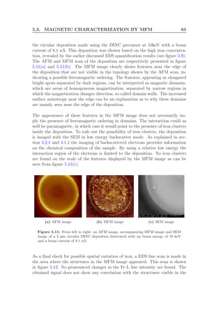
![5.2. EDS ANALYSIS 61
0 1 2 3 4 5
0.0
0.1
0.2
0.3
0.4
0.5
0.6
0.7
0.8
0.9
1.0
energy (keV)
k-ratio
O K
C K
Fe L
Si K
(a) TIDC deposition of 7 nm thickness
0 1 2 3 4 5
0.0
0.1
0.2
0.3
0.4
0.5
0.6
0.7
0.8
0.9
1.0
energy (keV)
k-ratio
O K
C K
Fe L
Si K
(b) DINC deposition of 70 nm thickness
Figure 5.7: K-ratio versus energy plots calculated by Stratagem for a 7 nm thick TIDC
deposition (a) and a 70 nm thick DINC deposition (b) on Si.
measurements where done on a new set of depositions fabricated under the exact
same conditions, but with exposure to air after deposition. The exposure to air
was a consequence of AFM measurements performed on this set of depositions.
The composition of the depositions was determined in Stratagem using the k-
ratios of the Fe L, O K and C K lines. The results are shown in figures 5.8 and
5.9.
We will first discuss the implications of these results on the reliability of EDS thin
film analysis, before interpreting the results with respect to EBID. The quantifi-
cation of the TIDC depositions at 2.5 and 4 keV are consistent within an error
of a few percent, even though the energy of 4 keV does not optimally match the
thickness of the depositions (see figure 5.7(a)). Based on this observation it is
expected that EDS quantification of thin films can be assumed to be accurate
within a few percent as long as the used energy is within the same range as the
optimal energy. A higher accuracy may even be obtained when the used energy
optimally matches with the thickness of the sample.
The background in the graphs of figure 5.8 has been colored by means of three
horizontal bands to emphasize the fact that the composition of these TIDC depo-
sitions does not change significantly with the electron beam current. In literature
[13, ?] it is generally seen that with increasing beam current, the purity of EBID
depositions increases as well. The mechanism responsible for this effect can be
understood in terms of the dissipated energy and consequent more complete de-
composition. Moreover, the dissipated energy could lead to heating, thereby
purifying the depositions through a process called annealing4
. None of these pro-
4
Annealing is a general term for a heat treatment to alter material properties.](https://image.slidesharecdn.com/f1d9af8f-520d-4711-b40c-d67fd4a14028-161106155501/85/Graduation-Thesis-TUe-Michael-Beljaars-69-320.jpg)

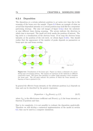
![68 CHAPTER 6. MODELING EBID
(a) SEM image of a square deposi-
tion
0
0.5
1
1.5
2
0
0.5
1
1.5
2
0
10
20
30
40
50
length (µm)width (µm)
height[nm]
(b) 3D view of an AFM image of the same deposition as
in (a)
Figure 6.1: SEM (a) and AFM (b) images of a 300s square deposition with a beam
energy of 5 keV and a beam current of 1.6 nA.
to a high surface occupation N. In the opposite case, a lower surface occupation
will be realized. Diffusion depends on a barrier for diffusion Ediff , which is in
general smaller than Eads, and on the local gradient in the surface occupation.
In case of a homogeneous occupation, diffusion does not have an effect on the
surface occupation.
In the case of EBID we locally modify the properties of the substrate by cre-
ating a deposition, which changes the energy barriers of the surface processes.
The modification of the area of deposition occurs in the first few passes of the
deposition. Since a typical deposition consists of thousands of passes, this mod-
ification can be considered instantaneous. The magnitude of this change will
depend on the used substrate and precursor. Considering Eads we can distin-
guish between two extremes as depicted in figure 6.2a. Either the barrier is lower
on the deposition compared to the barrier (left side of the figure) on the sub-
strate or vise versa (right side). This difference in Eads leads to a difference in N
between the deposition and the substrate as can be seen in figure 6.2b.
The gradient at the transition between substrate and deposition makes that dif-
fusion starts to play a role. Diffusion will cause a gradual change between the
different surface occupations, as visualized in the figure, leading to an new equi-
librium occupation in the transition region. The width of the transition will
depend on the occupation gradient ∇N and the diffusion energy barrier Ediff .](https://image.slidesharecdn.com/f1d9af8f-520d-4711-b40c-d67fd4a14028-161106155501/85/Graduation-Thesis-TUe-Michael-Beljaars-76-320.jpg)

![6.2. ANALYTICAL MODEL 75
6.2.5 Final expression
Substituting the expressions for adsorption (6.3), desorption (6.5), diffusion (6.15)
and deposition (6.17) in equation 6.1, the differential equation takes the shape of
dN
dt
=
Nm − N
Nm
· PF [1 − pdes] − νdNpdes + D · ∇2
N − SdepBeam(x, y, t)N.
(6.18)
where pads is replaced by 1 − pdes. By ordering the terms as function of N and
its derivatives, we obtain
dN
dt
= D · ∇2
N −
PF[1 − pdes]
Nm
+ νdpdes − SdepBeam(x, y, t N + PF [1 − pdes] .
(6.19)
If we take into account only adsorption and desorption, this equation 6.19 reduces
to
dN
dt
= PF [1 − pdes] −
PF[1 − pdes]
Nm
+ νdpdes N. (6.20)
We will see in the next section that we can use this last equation to calculate
equilibrium occupations on the substrate and on the deposition, far from the
region where diffusion plays a role.
6.2.6 Implications of the model
We can study part of the effect of diffusion by looking at the difference between
the equilibrium occupation at the substrate Ns
eq and the deposition Nd
eq. Far from
the boundary between substrate and deposition, the equilibrium condition will
not depend on diffusion and can be found by equating equation 6.20 to zero. This
leads to
Neq =
1
1
Nm
+ pdes
[1−pdes]
νd
P F
. (6.21)
Substituting the respective energy barriers in expression 6.21 we obtain the equi-
librium occupations Ns
eq and Nd
eq. The variable of interest is R, the difference
between the two surface occupations relative to the surface occupation on the
deposition, because this gives an estimate of the extent to which the discussed
features are visible. The expression for R is given by](https://image.slidesharecdn.com/f1d9af8f-520d-4711-b40c-d67fd4a14028-161106155501/85/Graduation-Thesis-TUe-Michael-Beljaars-83-320.jpg)
![76 CHAPTER 6. MODELING EBID
R =
Ns
eq − Nd
eq
Nd
eq
=
Ns
eq
Nd
eq
− 1 (6.22)
=
1
Nm
+
pd
des
[1−pd
des]
νd
P F
1
Nm
+
ps
des
[1−ps
des]
νd
P F
− 1. (6.23)
From this formula, it can be seen that we can distinguish between two extremes.
For the condition
PF >>
pdes
1 − pdes
νdNm (6.24)
R reduces to zero. In this condition pdes is the larger of the two desorption
chances. This means that for high particle fluxes compared to the maximum
occupation, the equilibrium occupation on both the substrate and the deposition
are equal to the maximum occupation. Consequently the difference between the
two reduces to zero.
The other extreme is found for the condition
PF <<
pdes
1 − pdes
νdNm (6.25)
where pdes is the smaller of the two desorption chances. Under this condition R
simplifies to
R =
pd
des
[1−pd
des]
ps
des
[1−ps
des]
− 1 =
1 − pd
des
[1 − ps
des]
pd
des
ps
des
− 1. (6.26)
The derived expression depends only on the adsorption and desorption chances,
which themselves are a function of energy barriers and temperature. For a given
precursor - substrate combination, the energy barriers are fixed and consequently
expression 6.26 is only a function of temperature.
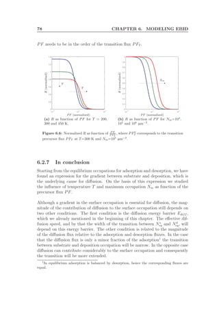
In figure 6.5 the normalized expression for R is plotted as function of PF, nor-
malized with respect to the transition flux PFT . This is the flux at which the
transition between the two regimes discussed above takes place. An expression
for the transition precursor flux can be found by calculating the second derivative
of R with respect to log(PF) and subsequently equating the obtained expression](https://image.slidesharecdn.com/f1d9af8f-520d-4711-b40c-d67fd4a14028-161106155501/85/Graduation-Thesis-TUe-Michael-Beljaars-84-320.jpg)
![6.2. ANALYTICAL MODEL 77
to zero. The transition precursor flux is given by
ps
des
1−ps
des
νdNm, as shown in the
figure by the vertical dashed line. On the left side R converges to the limit for a
low precursor flux. The derived value for this limit is indicated in the figure. On
the right side it can be seen that the curve approaches zero, the limit for a high
precursor flux.
10
0
10
5
10
5
0
0.1
0.2
0.3
0.4
0.5
0.6
0.7
0.8
0.9
1
P F (normalized)
R(normalized)
1−pd
des
[1−ps
des]
pd
des
ps
des
− 1
0
P F << pdes
1−pdes
νdNm
P F >> pdes
1−pdes
νdNm
ps
des
1−ps
des
νdNm
Figure 6.5: A plot of R, normalized, as function of PF, normalized with respect to the
transitions precursor flux PFT . Indicated in the figure are the conditions and values for
the limits discussed in the text. Furthermore the analytical expression for the transition
precursor flux is shown.
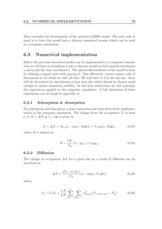
In figure 6.6 plots are shown of R versus PF, for different values of the substrate
temperature T (figure 6.6(a) and maximum occupation Nm (figure 6.6(b)) to
study their effect on R. The middle curve of both plots is normalized along the x
axis with respect to the precursor transition flux and along the y axis with respect
to its maximum. The other curves are scaled with the normalization factors of
the middle curve. has been The arrows in the figures indicate the direction in
which the relevant parameter increases. From figure 6.6(a) it can be seen that
increasing the temperature, leads to a decrease of R in the precursor flux lim-
ited regime and a slight shift of the transition flux PFT towards a higher value.
Consequently it can be expected that the extent to which deposition features are
present is diminished. The variation of Nm causes a shift of the curve along the
x-axis. For smaller Nm than Nm of the normalization curve, the curve shifts to
lower values of PF and visa versa. In contrast to the temperature, the maximum
occupation, being based on the spatial extent of a precursor molecule, is not a
parameter that can easily be controlled. In principle the value for Nm for a given
precursor is fixed, but may be influenced by the presence of other molecules. For
a change in Nm to be reflected in deposition characteristics, the precursor flux](https://image.slidesharecdn.com/f1d9af8f-520d-4711-b40c-d67fd4a14028-161106155501/85/Graduation-Thesis-TUe-Michael-Beljaars-85-320.jpg)

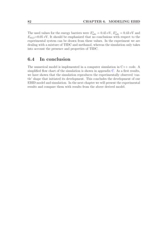
![6.3. NUMERICAL IMPLEMENTATION 81
delay
delay
(a)
intensity(a.u.)
time (a.u.)]
(b)
Figure 6.7: Visualization of a discretized beam spot. (a) shows a schematic of a
discrete meandering type of scanning pattern. The large squares are instances of the
substrate at different consecutive times. The small squares the substrate is build of are
the discretization bins. The green (low intensity) and yellow (high intensity) square
visualizes the beam spot. The small red squares indicate the position of which the beam
intensity as function of time is plotted in (b).
used value for the precursor flux PF of TIDC was calculated from the vapor
pressure and GIS flow conductance, as explained in section 4.1.3. The maximum
occupation Nm was calculated based on the surface coverage of a TIDC molecule.
The result of this simulation is shown in figure 6.8.
0
20
40
60
80
0
20
40
60
80
0
5
10
15
20
0
2
4
6
8
10
12
14
16
length (bins)
width
(bins)
height(a.u.)
Figure 6.8: Simulation of a square deposition.
The shape of the simulation matches well with the experimentally observed shape.](https://image.slidesharecdn.com/f1d9af8f-520d-4711-b40c-d67fd4a14028-161106155501/85/Graduation-Thesis-TUe-Michael-Beljaars-89-320.jpg)

![100 CHAPTER 9. OUTLOOK
9.2.1 In situ treatment
In the experiments in chapter 7 heating of the substrate was used to study dif-
fusion. Heating of the substrate may also enhance the purity of the depositions.
Aided by the raised substrate temperature, the threshold for decomposition is
easier to overcome. If the substrate temperature is set too high, decomposition
will take place independent of the electron beam by merely thermal decomposi-
tion. It is expected that, below this limit, there exist an optimal temperature
with respect to the purity of the depositions. Increasing the substrate temper-
ature may also affect the diffusion of contaminants such as carbon out of the
depositions. This effect will contribute to the enhancement of the purity.
A technique in literature [16] that has been proven to decrease carbon content
is the addition of water vapor during depositing. The water molecules dissociate
into radicals under irradiation with the electron beam and subsequently bind to
carbon. Because of the volatile nature of the radicals, they have a high proba-
bility of leaving the deposition. The removal of carbon occurs at the cost of the
incorporation of additional oxygen.
An alternative to using water vapor is the application of a hydrogen gun. By
means of this gun, atomic hydrogen is supplied to the deposition area. In a sim-
ilar way as in the case of water vapor, carbon is removed from the depositions.
The great advantage of the hydrogen gun is that it does not lead to incorporation
of additional oxygen.
9.2.2 Ex situ treatment
To improve the purity after deposition, the depositions can be given a specific
heat treatment to distil the pollutants from the deposition. Such a heat treatment
is generally referred to as annealing. The environment in which annealing is
performed is of importance for the purifying. Therefore generally ultra high
vacuum (UHV) or argon atmosphere are chosen to perform the annealing process.
Annealing may not only improve purity, but it can also lead to an enhancement of
other properties such as the magnetic properties and the electrical conductivity.
In the next section we will present preliminary results on the measuring of the
electrical conductivity of the TIDC depositions before and after annealing in
UHV as an outlook for further research.
9.3 Electrical characterization
In a first attempt to characterize the electrical conductivity of the TIDC deposi-
tions, annealing was applied. To measure the resistances, rectangular 5 x 1 µm
depositions were fabricated between two gold electrodes shown in figure 9.1(b).](https://image.slidesharecdn.com/f1d9af8f-520d-4711-b40c-d67fd4a14028-161106155501/85/Graduation-Thesis-TUe-Michael-Beljaars-108-320.jpg)
![References
[1] Multiple Authors. Histories of the Electron. MIT Press, 2001.
[2] S. Goudsmit and G. E. Uhlenbeck. Die Kopplungsm¨oglichkeiten der Quan-
tenvektoren im Atom. Zeitschrift fur Physik, 35:618–625, August 1926.
[3] L. H. Thomas. The Motion of the Spinning Electron. Nature, 117:514, April
1926.
[4] S. Goudsmit. The discovery of the electron spin, 1971. Closing lecture at
the golden jubilee of the Dutch Physical Society in 1971
http://www.optics.arizona.edu/opti511r/HW/goudsmit_lecture.pdf
http://www-lorentz.leidenuniv.nl/history/spin/goudsmit.html.
[5] J. Mauritsson, P. Johnsson, E. Mansten, M. Swoboda, T. Ruchon,
A. L’Huillier, and K. J. Schafer. Coherent electron scattering captured by
an attosecond quantum stroboscope. Physical Review Letters, 100(7):073003,
2008.
[6] S. Chatterjee. Heisenberg and ferromagnetism. Resonance, pages 57–66,
August 2004.
[7] T. Lukasczyk, M. Schirmer, H. Steinrck, and H. Marbach. Electron-beam-
induced deposition in ultrahigh vacuum: Lithographic fabrication of clean
iron nanostructures. Nanolithography, 4(6):841, 2008.
[8] J. F. Ziegler. SRIM-2003. Nuclear Instruments and Methods in Physics
Research B, 219:1027–1036, June 2004.
[9] Dany Joly Xavier Tastet Vincent Aimez Raynald Gauvin Dominique Drouin,
Alexandre Ral Couture. Casino v2.42-a fast and easy-to-use modeling
tool for scanning electron microscopy and microanalysis users. Scanning,
29(3):92–101, 2007.
[10] E. Kerr, S. van Dijken, R. M. Langford, and J. M. D. Coey. Effects of Ga+
ion implantation on the magnetoresistive properties of spin valves. Journal
of Magnetism and Magnetic Materials, 290:124–126, April 2005.
[11] D. Ozkaya L, R. M. Langford, W. L. Chan, and A. K. Petford-Long. Effect of
Ga implantation on the magnetic properties of permalloy thin films. Journal
of Applied Physics, 91:9937–9942, June 2002.
102](https://image.slidesharecdn.com/f1d9af8f-520d-4711-b40c-d67fd4a14028-161106155501/85/Graduation-Thesis-TUe-Michael-Beljaars-110-320.jpg)
![REFERENCES 103
[12] R. R. Kunz, T. E. Allen, and T. M. Mayer. Selective area deposition of met-
als using low-energy electron beams. Journal of Vacuum Science & Tech-
nology B: Microelectronics and Nanometer Structures, Volume 5, Issue 5,
September 1987, pp.1427-1431, 5:1427–1431, September 1987.
[13] M. Shimojo, M. Takeguchi, M. Tanaka, K. Mitsuishi, and K. Furuya. Elec-
tron beam-induced deposition using iron carbonyl and the effects of heat
treatment on nanostructure. Applied Physics A: Materials Science & Pro-
cessing, 79:1869–1872, December 2004.
[14] M. Takeguchi, M. Shimojo, and K. Furuya. Fabrication of magnetic nanos-
tructures using electron beam induced chemical vapour deposition. Nan-
otechnology, 16:1321–1325, August 2005.
[15] R. C. Che, M. Takeguchi, M. Shimojo, W. Zhang, and K. Furuya. Fabrication
and electron holography characterization of FePt alloy nanorods. Applied
Physics Letters, 87(22):223109, November 2005.
[16] M. Shimojo, M. Takeguchi, and K. Furuya. Formation of crystalline iron
oxide nanostructures by electron beam-induced deposition at room temper-
ature. Nanotechnology, 17:3637–3640, August 2006.
[17] M. Takeguchi, M. Shimojo, and K. Furuya. Nanostructure Fabrication by
Electron-Beam-Induced Deposition with Metal Carbonyl Precursor and Wa-
ter Vapor. Japanese Journal of Applied Physics, 46:6183, September 2007.
[18] K. Furuya, M. Takeguchi, and K. Mitsuishi. Iron nanostructures fabricated
by electron beam induced deposition and its magnetic properties. Solid State
Phenomena, 124-126:139–142, 2007.
[19] M. Takeguchi, M. Shimojo, and K. Furuya. Fabrication of a nano-magnet
on a piezo-driven tip in a tem sample holder. Journal of Materials Science,
41:2627–2630, 2006.
[20] M. A. Bruk, E. N. Zhikharev, E. I. Grigoriev, A. V. Spirin, V. A. Kalnov,
and I. E. Kardash. Focused Electron Beam-Induced Deposition of Iron
and Carbon-containing Nanostructures from Triiron Dodecacarbonyl Vapor.
High Energy Chemistry, 39:93–96, 2005.
[21] J. M¨uller, S. von Moln´ar, and S. Wirth. Room temperature magnetore-
sistance switching of Permalloy thin films induced by iron nanoparticles.
Applied Physics Letters, 92(9):093121, March 2008.
[22] C. W. Oatley. The early history of the scanning electron microscope. Journal
of Applied Physics, 53, February 1982.](https://image.slidesharecdn.com/f1d9af8f-520d-4711-b40c-d67fd4a14028-161106155501/85/Graduation-Thesis-TUe-Michael-Beljaars-111-320.jpg)
![104 REFERENCES
[23] A. N. Broers, W. W. Molzen, J. J. Cuomo, and N. D. Wittels. Electron-beam
fabrication of 80-˚A metal structures. Applied Physics Letters, 29:596–598,
November 1976.
[24] Randolph, S. J., Fowlkes, J. D., Rack, and P. D. Focused, nanoscale electron-
beam-induced deposition and etching. Critical Reviews in Solid State and
Material Sciences, 31(3):55–89, September 2006.
[25] Natalia Silvis-Cividjian. Electron Beam Induced Nanometer Scale Deposi-
tion. PhD thesis, Technische Universiteit Delft, 2002.
[26] Daryl Allen Smith. Elucidating the Growth Mechanisms of Electron Beam
Induced Deposition via a Three Dimensional, Monte Carlo Based Simulation.
PhD thesis, University of Tennessee, 2007.
[27] David C. Joy Yinghong Lin. A new examination of secondary electron yield
data. Surface and Interface Analysis, 37(11):895–900, 2005.
[28] J. Goldstein, D. Newbury, D. Joy, C. Lyman, P. Echlin, E. Lifshin,
L. Sawyer, and J. Michael. Scanning Electron Microscopy and X-ray Mi-
croanalysis. Springer, third edition, 2003.
[29] M. Beljaars. Imaging of domain walls in small shape anisotropy dominated
magnetic structures. Technical report, Technische Universiteit Eindhoven,
2005.
[30] R. Wiesendanger and H. J. G¨untherodt. Scanning Tunneling Microscopy II.
Springer-Verlag, 1992.
[31] M. M. H. Willekens. Giant Magneto Resistance in Spin Valves. PhD thesis,
Technische Universiteit Eindhoven, 1997.
[32] prof.dr.ir. H.J.M. Swagten. Magnetism & magnetic materials. course syl-
labus, 2005.
[33] J. Jongen. Quantitative magnetic force microscopy: determining the mag-
netic moment of a mfm tip. Technical report, Technische Universiteit Eind-
hoven, 2008.
[34] J. Pouchou. X-ray microanalysis of stratified specimens. Analytica Chimica
Acta, 283(1):81, 1993.](https://image.slidesharecdn.com/f1d9af8f-520d-4711-b40c-d67fd4a14028-161106155501/85/Graduation-Thesis-TUe-Michael-Beljaars-112-320.jpg)
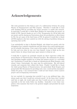

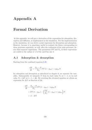
![110 APPENDIX A. FORMAL DERIVATION
Ni+∆N
Ni
dN
A − BN
=
ti+∆t
ti
dt
−
1
B
ln (A − BN)
Ni+∆N
Ni
= ∆t
ln
A − B (Ni + ∆N)
A − BNi
= −B∆t
A − B (Ni + ∆N) = (A − BNi) exp (−B∆t)
Ni + ∆N =
A
B
−
A
B
− Ni exp (−B∆t)
Ni + ∆N =
A
B
(1 − exp (−B∆t)) + Ni exp (−B∆t)
= Neq (1 − exp (−B∆t)) + Ni exp (−B∆t)
A.2 Adsorption
Analog to the combined equation for adsorption and desorption, we can solve the
differential equation
dN
dt
=
Nm − N
Nm
PF (1 − pdes)
for the adsorption. After the same operations as in previous derivation, we obtain
Nm
Nm − N
dN = PF (1 − pdes) dt
Ni+∆N
Ni
Nm
Nm − N
dN =
ti+∆t
ti
PF (1 − pdes) dt
−Nm ln [Nm − N]Ni+∆N
Ni
= [PF (1 − pdes) t]ti+∆t
ti
ln
Nm − Ni − ∆N
Nm − Ni
= −
PF
Nm
(1 − pdes) ∆t
Nm − Ni − ∆N = (Nm − Ni) exp −
PF
Nm
(1 − pdes) ∆t
∆N = (Nm − Ni) 1 − exp −
PF
Nm
(1 − pdes) ∆t .](https://image.slidesharecdn.com/f1d9af8f-520d-4711-b40c-d67fd4a14028-161106155501/85/Graduation-Thesis-TUe-Michael-Beljaars-118-320.jpg)
![A.3. DESORPTION 111
A.3 Desorption
The approach to the derivation of an numerical expression for the desorption is
similar to that of the adsorption. Starting from the adsorption equation from
chapter 6
dN
dt
= −νdpdesN,
we separate variables and integrate to obtain
1
N
dN = −νdpdesdt
Ni+∆N
Ni
1
N
dN =
ti+∆t
ti
−νdpdesdt
ln [N]Ni+∆N
Ni
= [−νdpdest]ti+∆t
ti
ln
Ni + ∆N
Ni
= −νdpdes∆t
Ni + ∆N = Ni exp (−νdpdes∆t)
∆N = Ni (exp (−νdpdes∆t) − 1) .
A.4 Diffusion
The numerical expression for diffusion as introduced in section 6.2.3 is given by
Diffusion = D · ∇2
N . (A.1)
We will first derive a numerical expression to calculate ∇2
N. In order to do this,
we will first look at calculating the first derivative. Numeric differentiation in bin
units is equivalent to calculating the difference between adjacent bins divided by
their distance d
N′
(x) =
N(x) − N(x + h)
d
(A.2)
N′
(i) =
N(i) − N(i + ∆i)
d∆i
(A.3)
=
N(i) − N(i + 1)
d
, (A.4)](https://image.slidesharecdn.com/f1d9af8f-520d-4711-b40c-d67fd4a14028-161106155501/85/Graduation-Thesis-TUe-Michael-Beljaars-119-320.jpg)
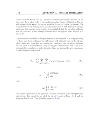
![A.4. DIFFUSION 113
dN
dt
=
1
8
D
d2
8
i=1
α2
i {Ni − N}
=
1
8
D
d2
4
i=1
{Ni − N} +
α2
8
D
d2
8
i=5
{Ni − N}
=
1
8
D
d2
4
i=1
{Ni} +
α2
8
D
d2
8
i=5
{DiNi} −
1
2
D
d2
N −
α2
2
D
d2
N
= C1 −
(1 + α2
) D
2d2
N
= C1 − C2N
After separation of the variables and subsequently integration over one time step
we obtain the expression
1
C1 − C2N
dN = dt
Ni+∆N
Ni
1
C1 − C2N
dN =
ti+∆t
ti
dt
−
1
C2
ln [C1 − C2N]Ni+∆N
Ni
= [t]ti+∆t
ti
ln
C1 − C2 (Ni + ∆N)
C1 − C2Ni
= −C2∆t
C1 − C2 (Ni + ∆N) = (C1 − C2Ni) exp (−C2∆t)
∆N =
(C1 − C2Ni)
C2
(1 − exp (−C2∆t)) .](https://image.slidesharecdn.com/f1d9af8f-520d-4711-b40c-d67fd4a14028-161106155501/85/Graduation-Thesis-TUe-Michael-Beljaars-121-320.jpg)
![Appendix B
Effective Beam Profile
Most EBID simulations use Monte Carlo based models1
to simulate the electron
- solid interactions. These simulations were developed to investigate the ultimate
resolution of EBID [25] or to simulate nanometer sized depositions [26]. For these
small scales Monte Carlo is a suitable technique, however for the micrometer sized
depositions investigated in this thesis this method is unfit. Therefore we will de-
velop an alternative way to describe the deposition process as function of surface
occupation. We will call this description the effective beam profile.
A way to investigate the interaction of an electron beam with a substrate is
by means of a Monte Carlo simulation. Figure B.1 shows the trajectory of the
primary electrons (PE) in a Si substrate for a 2 keV beam and a 15 keV beam.
The figures are made with a freeware Monte Carlo based simulation program
called Casino [?].
From figure B.1(a) and B.1(b) it is clear that the penetration depth and scatter
width of the PE’s depend on their energy, which will affect the amount of energy
dissipated at a certain position. The amount of SE’s that will be generated at a
certain position in the substrate depends on the amount of energy dissipated by
the PE’s. In this respect it is useful to define surfaces of constant dissipated en-
ergy, so called isosurfaces of dissipated energy. The shape of these isosurfaces can
be described as droplet shaped shells as can be seen in figures B.1(c) and B.1(d).
Although these surfaces differ in size for different PE energies, their overall shape
remains the same. This will greatly simplify the description of an effective beam
profile as function of the energy of the primary electrons.
For describing the electron beam as an effective beam profile at the surface of
the substrate, it is necessary to know the amount and energy of secondary elec-
trons that arrive at the surface after generation in the substrate. We assume
here, as already mentioned in chapter 3, that deposition is mainly induced by
the secondary electrons. Because Casino does not calculate the generation and
trajectory of the secondary electrons, we will use the simple straight line approxi-
1
Monte Carlo simulations are based on the tracing of every PE trajectory and subsequently
generated SE trajectory.
114](https://image.slidesharecdn.com/f1d9af8f-520d-4711-b40c-d67fd4a14028-161106155501/85/Graduation-Thesis-TUe-Michael-Beljaars-122-320.jpg)
![115
(a) PE trajectory of 2 keV electrons, inset
displays an enlargement of the same simula-
tion
(b) PE trajectory of 15 keV electrons
(c) Sliced view of isosurfaces of 2 keV elec-
trons
(d) Sliced view of isosurfaces of 15 keV elec-
trons
Figure B.1: Monte Carlo simulations of electrons in Silicon
mation [25] for the transport of SE’s towards the surface. The assumptions made
in this model are that SE move in straight paths to the surface and that scattered
SE are immediately adsorbed. The equation
p(E, z0) = e
−
z0
λinel(E)cos(θ)
(B.1)
describes the chance for an electron generated at depth z0 and moving in a di-
rection θ to reach the surface unscattered. The parameter λinel is the inelastic
mean free path of the electron and is given by the equation [25]
λinel(E) = a0 ∗
538
(E − EF )2
+ 0.72(a0(E − EF ))1/2
(B.2)](https://image.slidesharecdn.com/f1d9af8f-520d-4711-b40c-d67fd4a14028-161106155501/85/Graduation-Thesis-TUe-Michael-Beljaars-123-320.jpg)

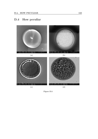


![[A. hobbacher] fatigue_design_of_welded_joints_and](https://cdn.slidesharecdn.com/ss_thumbnails/a-160512092007-thumbnail.jpg?width=640&height=640&fit=bounds)


