
Recommended
Recommended
More Related Content
Similar to FIRST REVIEW-2 of the dcd dcd consjsks.pptx
Similar to FIRST REVIEW-2 of the dcd dcd consjsks.pptx (20)
More from NirmalM15
More from NirmalM15 (7)
Recently uploaded
Recently uploaded (20)
FIRST REVIEW-2 of the dcd dcd consjsks.pptx
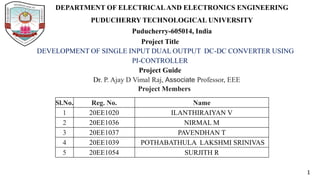
- 1. DEPARTMENT OF ELECTRICALAND ELECTRONICS ENGINEERING PUDUCHERRY TECHNOLOGICAL UNIVERSITY Puducherry-605014, India Project Title DEVELOPMENT OF SINGLE INPUT DUAL OUTPUT DC-DC CONVERTER USING PI-CONTROLLER Project Guide Dr. P. Ajay D Vimal Raj, Associate Professor, EEE Project Members Sl.No. Reg. No. Name 1 20EE1020 ILANTHIRAIYAN V 2 20EE1036 NIRMAL M 3 20EE1037 PAVENDHAN T 4 20EE1039 POTHABATHULA LAKSHMI SRINIVAS 5 20EE1054 SURJITH R 1
- 2. CONTENT ➢ INTRODUCTION ➢ OBJECTIVE ➢ EXISTING WORK ➢ BLOCK DIAGRAM ➢ IMPLEMENTED WORK ➢ DESIGN VALUES ➢ PI-CONTROLLER DESIGN ➢ OPEN LOOPANALYSIS ➢ CLOSED LOOP ANALYSIS ➢ WORK PLAN ➢ CONCLUSION 2
- 3. Introduction ❖ A single-input, dual-output (SIDO) DC-DC converter is a type of power electronics circuit that takes a single input voltage and concurrently generates dual output voltages. ❖ The loads are isolated in SIDO converters; therefore, they can regulate the output voltage independently. ❖ This type of converter is commonly used in applications where multiple voltage rails are required, such as automotive electronics, embedded systems, renewable energy systems, etc..
- 4. Objective ➢ To eliminate the cross regulation problem that exist in the conventional approach. ➢ To design the single input dual output DC -DC converter using PI controller that can obtain the desired output voltage level using simulink in MATLAB. ➢ To implement the SIDO DC-DC converter using PI controller in Prototype module.
- 5. EXISTING WORK The SIDO DC-DC converter generates two outputs: one is boost, and another is buck-boost. The main flaw in this conventional approach is the cross-regulation problem, and the loads are not being isolated from each other while they are operating. If the ground is implicated, there is a possibility of grounding problems when charging the battery while concurrently turning on loads.
- 6. + - 𝐾𝑝 𝑘𝑖 𝛴 + + Set point DC-DC Converter LOAD K PWM K PI-CONTROLLER Feedback Gain DC-LOAD 𝑽𝟎 𝑽𝟎 ERROR BLOCK DIAGRAM
- 7. IMPLEMENTED WORK 1 2 BOOST CONVERTER BUCK-BOOST CONVERTER PI- CONTROLLER PI- CONTROLLER SINGLE INPUT, DUAL OUTPUT DC-DC CONVERTER
- 8. DESIGN VALUES INPUT VOLTAGE(𝑣𝑖𝑛) = 24V SWITCHING FREQUENCY(𝑓𝑠)=50KHz BOOST CONVERTER 𝑉 𝑐𝑝𝑝 = 𝑉 𝑟/2 1.Inductance L =2𝑅𝐿𝑚𝑎𝑥/27𝑓𝑠 =2*337.5/27*50000 L1 = 0.5*10−3 H 2.Capacitance C =𝐷𝑚𝑎𝑥 ∗ 𝑉01/𝑉 𝑐𝑝𝑝* 𝑅𝐿𝑚𝑎𝑥* 𝑓𝑠 =0.9*240/0.1*337.5*50000 C1 = 128*10−6 F 𝑉01= 𝑉𝑖𝑛/(1 − D) BUCK-BOOST CONVERTER 𝑉 𝑐𝑝𝑝 = 𝑉 𝑟/2 1.Inductance L = 𝑅𝐿𝑚𝑎𝑥 ∗ (1 − 𝐷𝑚𝑖𝑛)/2𝑓𝑠 = 111.53(1-0.1)/2*50000 L2 = 1*10−3 H 2.Capacitance C =𝐷𝑚𝑎𝑥 ∗ 𝑉02/𝑉 𝑐𝑝𝑝* 𝑅𝐿𝑚𝑎𝑥* 𝑓𝑠 =0.9*216/0.1*111.53*50000 C2 = 348*10−6 F 𝑉02= 𝑉𝑖𝑛 ∗ D/(1 − D) INDUCTANCE(L) CAPACITANCE(C) L1 = 0.5*10−3 H C1 = 128*10−6 F L2 = 1*10−3 H C2 = 348*10−6 F
- 9. DESIGN OF PROPORTIONAL AND INTEGRAL GAIN: Ziegler- Nichols Method TYPE OF CONTROLLER 𝐾𝑝 𝑇𝑖 𝑇𝑑 PI 0.45𝐾𝑐𝑟 1/1.2𝑃c𝑟 0 𝐾𝑐𝑟=0.0011 𝐾𝑝=0.0005 𝑃c𝑟=0.0022s 𝑇𝑖=0.00183 𝐾𝑝 = K 𝐾𝑖 = K/𝑇𝑖 𝐾𝑖 = 0.2 𝐾𝑝=0.0005 Therefore, proportional gain and integral gain 𝐾𝑖 = 0.2 Where, 𝐾𝑐𝑟 ⇒ Critical gain 𝑃c𝑟 ⇒ Critical period 𝐾𝑝 ⇒ Proportional gain 𝐾𝑖 ⇒ Integral gain 𝑇𝑖 ⇒ Integral time
- 10. OPEN LOOP SIMULATION RESULTS Duty ratio Boost Buck-Boost Output(𝑽𝟎) Ripple Output(𝑽𝟎) Ripple
- 11. OPEN LOOPANALYSIS BOOST CONVERTER
- 13. CLOSED LOOP SIMULATION RESULTS LOAD Boost Buck-Boost Output(𝑽𝟎) Ripple Output(𝑽𝟎) Ripple
- 14. CLOSED LOOPANALYSIS BOOST CONVERTER
- 16. WORK PLAN SI.NO WORK TIME LINE STATUS 1. Finalizing the project title and base paper. 2 weeks Completed 2. Preparing literature paper survey. 1 week Completed 3. To design a simulation model for SIDO dc-dc converter. 2 weeks Completed 4. Analyze the performance with open loop control. 1 week Completed 5. To design PI-controller in MATLAB-Simulink. 1 week Completed 6. Analyze the performance in closed loop control using PI-controller 1 week Completed 7. Study about components needed for prototype module. 1 week 8. Hardware implementation of closed loop control 3 weeks 9. Result analysis and conclusion of project 2 weeks 10. Final report preparation 2 weeks
- 17. CONCLUSION The implemented SIDO DC - DC converter structure can generate boost and buck-boost output voltages with independent regulated voltage. In Improved DC-DC converter, the energy stored in the inductor is confined to one output only and is not shared with other outputs. During control the loads are segregated from one another, and the cross regulation problem is successfully resolved. So, the output voltages are unaffected by sudden changes in inductor and load currents . It permits to regulating the output voltages with independent duty-cycle. With the help of PI-CONTROLLER the desired output voltage can be obtained.