SlideShare a Scribd company logo
1 of 49
IOT BASED SMART WASTE SEGREGATOR MACHINE
Submitted in partial fulfillment of the requirements for the degree of
Bachelor of Technology
in
Electrical Engineering
By
SUMAN CHOWDHURY (2003602)
HITESH KUMAR BEHERA (2003603)
MALAY KUMAR MONDOL (2003608)
JAYAJIT KUMAR SAHOO (2003610)
Under the guidance of
School of Electrical Engineering,
KIIT Deemed to be University, Bhubaneswar.
April, 2021
ANIKT KUMAR SONI
AND
ANIL BEHERA
I hereby declare that the thesis entitled “ Design and analysis of a multilevel inverter with
boosting feature” submitted by me, for the award of the degree of Bachelor of Technology in
Electrical Engineering to KIIT is a record of bonafide work carried out by me under the
supervision of Prof. Tapas Roy.
I further declare that the work reported in this thesis has not been submitted and will not be
submitted, either in part or in full, for the award of any other degree or diploma in this institute or
any other institute or university.
Place : Bhubaneswar
Date : Anirban Jana
Anurag Sarkar
Arup Kumar Saha
Ishad Satyen
Signature of the Candidate
CERTIFICATE
This is to certify that the thesis entitled “Design and Analysis of multileveel inverter with
boosting feature” submitted by Anirban Jana, Anurag Sarkar, Arup kumar saha and Ishad
satyen bearing roll no 1703085, 1703091, 1703152 and 1703148 School of Electrical Engineering,
KIIT, Bhubaneswar, for the award of the degree of Bachelor of Technology in Electrical
Engineering , is a record of bonafide work carried out by him under my supervision, as per the
KIIT code of academic and research ethics.
The contents of this report have not been submitted and will not be submitted either in part
or in full, for the award of any other degree or diploma in this institute or any other institute or
university. The thesis fulfills the requirements and regulations of the University and in my opinion
meets the necessary standards for submission.
Place : Bhubaneswar
Date :
The thesis is satisfactory / unsatisfactory
Approved by
Evaluation Committee Chairman, PMC
Signature of the Guide
ACKNOWLEDGEMENT
We would like to express our deep sense of gratitude and appreciation to Prof. Tapas Roy for
constant and valuable suggestion, guidance, encouragement and influence for bringing out of this
project.
We would further thankful to the Prof. (Dr.) B. K. Nayak, Dean, School of Electrical Engineering,
all faculty members of school of Electrical Engineering and technical assistants of School of
Electrical Engineering for their constant support.We would like to thank our project mates, for
having many meaningful conversations and sharing those common thoughts together.
Anirban Jana 1703085
Anuraag Sarkar 1703091
Arup Kumar Saha 1703152
Ishad Satyen 1703148
Executive Summary
In this work, the symmetrical and asymmetrical topologies of cascaded multi-level inverter
(CMLI) are focused for a photo-voltaic (PV) system which is interconnected with grid through
a cascaded H-Bridge (CHB) inverter using suitable modulation technique. The simulation is
carried out using MATLAB/SIMULINK platform and total harmonic distortion (THD) level of
both topologies is compared which decides the suitability for practical applications. Further the
dynamic performance of a cascaded H-Bridge multilevel inverter (CHB-MLI) is described by
using dual loop cascaded controller for addressing various issues. It consists of two loops i.e.
outer loop and inner loop. The outer loop controller is a proportional-integral (PI) controller
used as a voltage controller and inner loop controller is a proportional (P) controller used as a
current controller. The steady state voltage i.e. constant output voltage with low THD is
achieved with the help of the voltage controller, while the transient/dynamic performance is
improved by using the current controller. The effectiveness of the controller has been tested on
both linear and non-linear loads. The detailed step-by-step procedures for designing the control
parameters of dual loop cascaded controller are given here. Finally, an optimal controller is
developed for a grid connected PV system to control the power from PV system to the utility
grid. The proposed controller ensures the unity power factor (UPF) operation as a result only
active power is injected into the grid. The simulation is carried out using
MATLAB/SIMULINK platform to evaluate the feasibility of the proposed controllers for
controlling the grid current.
CONTENTS Page No.
Acknowledgement i
Executive Summary ii
Table of Contents iii
List of Figures iv
List of Tables vi
Abbreviations viii
Symbols and Notations ix
S. No. Description Page No.
CHAPTER 1 INTRODUCTION 1
1.1 Background 2
1.2 Classical MLIs 11
1.3 Research Motivation 15
1.4 Research Objective 15
1.5 Survey Papers on MLIs 16
CHAPTER 2 PROJECT DESCRIPTION AND GOALS 22
2.1 Goals 22
2.2 Aim 22
2.3 Function 22
2.4 Methodology 23
CHAPTER 3 TECHNICAL SPECIFICATION 27
3.1 Technical Specification of MLIs 27
3.2 Analysis of the proposed design 27
CHAPTER 4 DESIGN APPROACH AND DETAILS 29
4.1 Circuit Description 29
4.2 Design Approach 29
4.3 Codes and standards 33
4.4 Constraints, Alternatives and Trade-Offs 33
CHAPTER 5 SCHEDULE, TASKS AND MILESTONES 35
5.1 Project Development Stage 26
5.2 Road Map 26
CHAPTER 6 PROJECT DEMONSTRATION 36
6.1 Simulation Results 36
6.2 Experiment Analysis 40
6.3 Results and Discussion 44
CHAPTER 7 COST ANALYSIS 46
CHAPTER 8 SUMMARY 42
REFERENCES 44
APPENDIX A (PROGRAMS) 47
APPENDIX B (GANTT CHART) 55
i
List of Figures
Figure No. Title Page No.
1.1 Configuration of Cascaded Multi-Level Inverter 8
1.2 Application areas of MLIs 11
1.3 Configuration of a Conventional Two-Level
Inverter
13
1.4 Cascaded H- bridge MLI 13
2.1 Proposed CHB-MLI 17
3.1 Gate pulse generation 20
4.1 Block Diagram of PI Controller 23
4.2 Equivalent Circuit Diagram for Determination
of Transfer Function
23
4.3 Principle of SPWM Technique 24
5.1 Road map 27
6.1 (a) Output Voltage (in Volt), (b) Load Current (in
Amp)
29
6.2 (a) Voltage THD, (b) Current THD 29
6.3 Gate pulse generation 30
ii
List of Tables
Table No. Title Page No.
1.1 Switching States of a 5-Level Inverter
8
1.2 Switching States of a 7-Level Inverter 9
1.3 Switching States of a 9-Level Inverter 10
1.4 Switching States of a 2-Level Inverter 13
2.1 Parameters for Design 19
4.1 IEEE-519 Standards for output voltage distortion 24
4.2
4.3
6.1
7.1
7.2
IEEE Standards for Current Distortion Limits
comparison of new 9 level CHB-MLI with other
9 level topologies
Filter and Controller Design Parameters for both
Linear and Non-Linear Loads
Cost estimation of components
Cost Analysis for the measuring instruments and
load
25
27
28
36
37
iii
List of Abbreviations
CMLI Cascaded Multilevel Inverter
PV Photo Voltaic
CHB Cascaded H-Bridge
THD Total Harmonic Distortion
CHB-MLI Cascaded H-Bridge Multilevel Inverter
V1 Input Voltage for Inverter 1
V2 Input Voltage for Inverter 2
Vd Magnitude of DC Input Voltage
PI Proportional-Integral
P Proportional
I Integral
UPF Unity Power Factor
DG Distribution Generation
MLI Multilevel Inverter
PWM Pulse Width Modulation
IGBT Insulated Gate Bipolar Transistor
VLinv Inverter Input Voltage
VAB Voltage across AB terminal
UPS Uninterruptible Power Supply
Kp Proportional Gain
Ki Integral Gain
fs Switching Frequency
ma Modulation Index
Vref Magnitude of Reference/Control Voltage Signal
Vcar Magnitude of Carrier Voltage Signal
SPWM Sinusoidal Pulse Width Modulation
iv
Symbols and Notations
SL NO. SYMBOL Meaning
1 Ω Ohm
2 ° Degree
3 H Henry
4 F Farad
5 V Volt
6 A Ampere
5
CHAPTER 1
INTRODUCTION
1.1 Background
Now-a-days most of the researchers have been focused on sources of renewable energy such
as wind, solar and hydro power plant to produce energy due to the high availability of such
energy in the world. A solar energy is considered as the best energy sources among all other
renewable sources on the basis of economic scale of production. The solar energy industry in
India is treated as fast growing plants. The government of Indian has already achieved the
target of 20 GW for the year 2022 in 2018 [1]. The present installed capacity of solar power
plant in India as of 30 Sept.19 is 31101 MW. The solar PV system has several advantages
such as robust, freely available in nature and long life periods as compared to other energy
sources. low maintenance and less production cost are the advantages so that the PV system
is considered as the best candidature of the sources. Moreover, solar PV system can be
interconnected with grid as a distribution generation (DG) system.
Inverters are power electronic modules that are dedicated to the conversion of the electrical
energy from DC power to AC power which is most used by today’s appliances. Inverters, in
the family of power electronic converters are gaining more interest today because of the
presence in most of renewable energy systems. With the advancement in semiconductor
devices and control techniques, the power electronic converters are becoming affordable with
better performances than before.
The applications of DC/AC converters are one of the widest as they cover from small power
applications such as portable devices, to high and medium power level applications such as
electric vehicles and renewable energy systems. The applications require converters to
produce better quality output voltage waveform. Further, the converter should be highly
efficient, simple in control and low cost. For that, improvements are necessary for an efficient
and better supply of power with high reliability and continuity. For different applications,
different types of inverter topologies have been proposed in this thesis. Considering the
output waveform, inverters are classified into [1]:
• Two levels inverter
• Three levels inverter
• Multilevel inverters (MLI)
6
In medium and high power applications, the conventional three-level PWM inverters are
becoming less popular because of their limitation to generate output voltage waveform with
high magnitude and lesser harmonic distortion. This limitation of PWM inverters is addressed
by increasing the switching frequencies. However, increasing switching frequencies create
efficiency and electromagnetic interference (EMI) problems because of the increment of
switching losses. To overcome these limitations, Multilevel Inverters (MLI) have been
proposed that are made up of power switches and some passive components to achieve
voltage of high magnitude that has lesser Total Harmonic Distortion (THD) and minimum
voltage stress across switches [2].
Generally, the solar panel available in the market has the efficiency of approximately 15-
20%. The power efficiency and the quality of the output volage waveforms can be enhanced
by using multilevel inverter (MLI). The solar PV system can be easily integrated with the
utility grid with the help of the MLI [2]. This method of generation can be used for the
medium to high power applications. In this work, the design and analysis of CMLI is carried
out for the solar PV applications and it may or may not integrate with the utility grid [3].
1.2 Overview of CHB MLIs
The cascaded H-bridge (CHB) configurations are commonly used as the effective classic
MLI topologies. These configurations comprises of two or more symmetrical single-phase H-
Bridge modules which is represented in Figure 1.1. These MLIs can produce an ac voltage
with required magnitude and frequency which has low total harmonic distortion (THD).
These topologies are useful for the high rated power with less THD and low switching losses
applications. The symmetric configuration of CHB MLIs can provide multiple number
output voltage levels with multiple controllable semiconductor switches. The asymmetric
topology of CHB MLIs with same number of switches can produce more output voltage
levels as compared to its symmetrical topology [4]. If V1, V2 … Vn are the voltage supplied
by the different PV panel to the indivisual H-n number of solar panels and the output voltage
is given by (1).
𝑉𝐴𝐵 = 𝑉01 + 𝑉01 + ⋯+ 𝑉𝑜𝑛 (1)
7
S11 S13
+
V1
-
S14 S12
+
V01
-
S21
+
S23
Output Voltag e
(VAB)
+
V2
-
S24 S22
V02
-
S21 S23
+
V2
-
S24 S22
+
V0n
-
Figure1.1: Configuration of Cascaded Multi-Level Inverter
1.2.1. CascadedMulti-LevelInverter (Symmetric)
In symmetrical configuration [5] same magnitude of DC supply are applied to the inverter.
𝑉1 = 𝑉2 = ⋯ = 𝑉n = 𝑉d
The number of voltage output levels (m) is evaluated by equatio (3).
(2)
𝑚 = 2𝑛 + 1 (3)
Where 𝑉𝑀 is maximum voltage produced.
𝑉𝑀 = 𝑛𝑉𝑑 (4)
e.g. if n=3 i.e. 3 H-Bridges were connected in cascaded, then it produces 7 levels of output
voltage [like -2Vd, -Vd, 0, Vd and 2Vd] with maximum value of voltage of 3Vd. Here, “0” and
“1” are represented for “On” and “Off” states of controllable switches.
TABLE 1.1: Switching States of a 5-Level Inverter
Switches
(VAB)
Voltage Level
Inverter 1 (V1= Vd) Inverter 2 (V2= Vd)
S11
S1
2
S1
3
S14
S2
1
S22
S2
3
S2
4
2Vd 1 1 0 0 1 1 0 0
Vd 1 1 0 0 0 1 0 0
0 0 1 0 1 0 1 0 1
-Vd 0 0 1 1 0 1 0 1
-2Vd 0 0 1 1 0 1 1 1
8
1.2.2. Cascaded Multi-Level Inverter (Asymmetric)
Due to application unequal magnitude of DC sources the configuration is known as
asymmetrical configuration. DC voltage magnitudes of ratio of either 1:2:4 or 1:3:9 are
applied.
1.2.3. Binary Asymmetrical MLI
If the ratio is 1:2:4, then it is called binary asymmetric MLI [5]. The value of dc source will
be evaluated by equation (5).
𝑉𝑛 = 2(𝑛−1)
𝑉𝑑 (5)
The number of voltage output levels (m) is determined by equation(6).
𝑚 = 2(𝑛+1) − 1 (6)
The maximum voltage produced is
𝑉𝑀 = (2𝑛 − 1)𝑉𝑑 (7)
e.g. if n=3 i.e. only 3 H-Bridges were cascaded, to produce 15 levels of output voltage .
Here, “0” and “1” are represented for “On” and “Off” states of controllable switches
respectively.
TABLE 1.2: 7-Level MLIs switching states
Switches
(VAB)
Voltage Level
Inverter 1 (V1= Vd) Inverter 2 (V2= 2Vd)
S11 S12 S13 S14 S21 S22 S23 S24
3Vd 1 1 0 0 1 1 0 0
2Vd 0 1 0 1 1 1 0 0
Vd 1 1 0 0 0 1 0 1
0 0 1 1 1 0 1 1 1
-Vd 0 0 1 1 0 1 0 1
-2Vd 0 1 0 1 0 0 1 1
-3Vd 0 0 1 1 0 0 1 1
9
1.2.4. Trinary Asymmetrical Multi-Level Inverter
If the ratio of DC voltage magnitudes is 1:3:9, then the configuration is called as trinary asymmetric MLI
[5]. The dc source value can be evaluated as
𝑉𝑛 = 3(𝑛−1)
𝑉𝑑 (8)
The number of voltage output levels (m) is calculated by equation(9).
𝑚 = 3𝑛 (9)
The maximum voltage evaluated is represented as
𝑉 =
3𝑛−1
𝑉 (10)
𝑀 2 𝑑
e.g. if n=3 i.e. 3 H-Bridges in cascaded connection generates 27 levels of output voltage
Here, “0” and “1” are represented for “On” and “Off” states of controllable switches.
TABLE 1.3: Switching States of a 9-Level Inverter
Switches
(VAB)
Voltage Level
Inverter 1 (V1= Vd) Inverter 2 (V2= 3Vd)
S11 S12 S13 S14 S21 S22 S23 S24
4Vd 1 1 0 0 1 1 0 0
3Vd 0 1 0 1 1 1 0 0
2Vd 0 0 1 1 1 1 0 0
Vd 1 1 0 0 0 1 0 1
0 0 1 0 1 0 1 0 1
-Vd 0 0 1 1 0 1 0 1
-2Vd 1 1 0 0 0 0 1 1
-3Vd 0 1 0 1 0 0 1 1
-4Vd 0 0 1 1 0 0 1 1
Merits of MLI over the conventional two level PWM inverters can be summarized as follow.
● MLI outputs are too close to sinusoidal waveform so that it has low THD.
●The dv/dt stress of MLI is too minimum compered to PWM inverters
● The stress in motor bearing, which use MLI control, is too low due to low common-mode
voltage of MLIs:
● MLI works using either fundamental or high switching frequency modulation scheme
10
1.3. Mainapplication area of MLIs
Different application area of MLIs are provided in Fig.1.5 [6].
Fig.1.2:Application areas of MLIs
MLI has some demerits such as it requires many number of power switches, capacitors gate
drivers, heat sinks, DC voltage sources which make it bulky, complex control circuit and
costly. Therefore, a number of studies are being conducted to improve them, while some are
seeking evolution of new structures, which have least number of power switches, capacitors,
gate driver, and DC supply. Moreover, in forging inverters there is an absence of voltage
boosting ability. So that the maximum output voltage is less than input voltage. To make the
output voltage magnitude greater than the input voltage, it is common to use either DC-to-DC
converter or inductor or transformer. However, these methods make the converter circuit
more complex, bulky, and less efficient. So that to improve the forgoing shortcomings of
MLIs Switched Capacitors (SC) is used in the MLI circuit in parallel/series fashion. The
capacitor stores charge when it is connected in parallel with the supply voltage. The capacitor
discharges its stored energy toward the load when it is connected in series with supply
voltage. The number of capacitors in MLI is decided by the magnitude of the output voltage.
In addition, SCMLI works either in fundamental switching frequency or in high switching
frequency modulation strategies. One of the major advantages of SCMLI structure is that the
structure does not require any complex control algorism to balance the capacitor voltages.
However, the SCMLI has the limitation of large requirement of power switches and passive
11
A
S1 S3
+
Vi,inv
Output Voltage
-
(V )
AB
Solar Panel
S4 S2
B
components as the output voltage level enhances. In addition, SCMLI has higher switching
stress and total standing voltage (TSV)
To solve the forging shortcomings of SCMLs, this this project work develops a novel inverter
structure, which reduces power device count considerably and boosts the output voltage. The
structure of this proposed topology compared with recently developed structures. The
effectiveness of the structure has been verified by MATLAB/Simulink.
1.3. ResearchMotivation
A MLI is a power electronics converter which provides required AC output voltage of
higher level using two or more DC voltages of lower level as an input. For designing such
inverter circuit, semiconductor switches are used. As IGBT (Insulated Gate Bipolar
Transistor) has high power rating, less conduction loss and less switching loss, it is used here
as a switch. Mostly a two-level inverter is used in order to generate the AC voltage from DC
voltage. The configuration of a two-level inverter is shown in Fig. 1. The MLI has advantages
over conventional two-level inverter [4, 6] such as increasing in number of voltage level
reduces the harmonic content and hence filter circuits required are reduced. Voltage stresses
on the device is less than that of the overall operating voltage. Thus, a high voltage waveform
can be obtained with switches having low rated voltage. It can be operated at both high
switching frequency and fundamental frequency, but low switching frequency can cause
reduce in switching loss with increase in efficiency. Also, grid without transformer can be
interconnected with such renewable sources of energy. MLIs can draw low distorted input
current compared to a two-level inverter.
Figure 1. 3: Configuration of a Conventional Two-LevelInverter
In Fig. 1 Vi,inv is the DC input voltage of the inverter taken from the solar panel. For the
inverter circuit shown in Fig. 1, the switching states are given in Table 1.4. Here, “0” and
“1” are represented for “On” and “Off” states of controllable switches.
12
TABLE 1.4: Switching States of a 2-Level Inverter
Switches
(VAB)
VoltageLevels
S1 S2 S3 S4
Vi,inv ON ON OFF OFF
0
ON OFF ON OFF
OFF ON OFF ON
-Vi,inv OFF OFF ON ON
All the controllers referred to in section 1.2 offer good performance. Among these controllers
PI controller is the most common used controller because it gives good result with easy
design which makes the analysis simpler than others
1.4. Research Objective
The ultimate goal of this dissertation is to develop an optimal controller so as to control
the power from solar PV to the utility grid and to maintain the power factor at UPF. Another
objective is to enhance the dynamic performance of the CHB-MLI by using dual loop
cascaded controller so that it can be used for various applications like uninterruptible power
supply (UPS) application and grid interconnection of solar PV system. The controller is
designed in such a way that it can be used for both linear load as well as non-linear load. It is
tested using MATLAB/SIMULINK platform with proper selection of controller parameters
i.e. proportional gain (Kp) and integral gain (Ki). Further it has been interconnected with grid
along with the loads. The effectiveness of the controller has been tested on both linear and
non-linear loads. The detailed step-by-step procedures for designing the control parameters
of dual-loop controller are given here. By the end of the thesis work, an optimal controller is
developed for a grid connected system to control the power from PV system to the utility
grid. The proposed controller ensures the UPF operation as a result only active power has
been pumped into the grid.
1.5. Surveyed Papers on MLIs
Some papers are related to the scope of renewable energy resources as given in [1]. In past
years, a sigle bridge inverter is used to convert the DC voltage into an AC voltage, which is
called as conventional two-level inverter and later MLI is used to convert the DC voltage to
AC voltage, which gives better performance compared to conventional two-level inverter as
given in [2], [4-9].
13
In some papers, various control strategies has been introduced for a grid connected inverter
system to control over the grid current. In most of the cases iterative learning control,
repetition dependent control and sliding mode control are suggested for pulse width
modulation (PWM) technique for improving the dynamic performance of the system as given
in [2-12], [13]. As the control scheme is voltage control, the output voltage waveform is
sensitive to the variation of load. Some researchers has suggested PI controllers to be used for
this control scheme as given in [14-16].
The paper [17] deals with simulation based comparison based on THD of the stand-alone
CHB MLI. Different configurations of CHB MLI, such as symmetrical and asymmetrical
configurations, are simulated by changing only the individual DC input voltages with the
same model having only two bridge inverters cascaded. In symmetrical configuration the
magnitudes of DC input voltages are same but in case of asymmetrical topology there are
two-types of configurations are present such as binary asymmetric configuration and trinary
asymmetric configuration as discussed in chapter 2. An asymmetric configuration of CHB-
MLI with two bridge inverters cascaded can generate more levels of output voltage with less
THD compare to other two configurations. In this paper, above mentioned all these
configurations are modelled with the same two-bridge inverter cascaded module with a
common pulse width modulation (PWM) technique using MATLAB/SIMULINK platform
and their THD is compared for different switching frequency (fs) and different modulation
index (ma).
The paper [18] explores the control techniques for the stand-alone CHB MLI, which can be
implemented for UPS Applications or can be interconnecting the solar PV system with the
utility grid to transfer only active power from the solar to the grid at UPF. A UPS system is
used for protecting the equipments like computers and medical devices from data loss caused
by power failure interruption i.e. it can be used for any load either linear load or non-linear
load. Hence, to improve the efficiency of UPS, an optimal dual loop cascaded controller is
modelled in this paper and it is tested using MATLAB/SIMULINK platform.
1.6. Organization of Thesis
This thesis work is organised with the following five chapters. Chapter 1 introduces about the
thesis work which consists of introduction, literature review, motivation and objective.
Chapter 2 is about analysis of CHB-MLI which contains different topologies of CHB inverter
along with their switching states and their performance based comparisons are described.
14
Chapter 3 indicates the modulation techniques used for the switching of the inverter. It
emphasizes different types of modulation techniques and the simulation of preferred
modulation technique. In chapter 4, control of CHB-MLI for UPS application is discussed. In
this section the UPS system, controller design for UPS and the simulation of the complete
system for different loads are described. Chapter 5 elaborates the grid connected PV system.
It includes the design of the controller for the grid current to maintain the power factor at
UPF and it is tested using MATLAB/SIMULINK platform. Finally it concludes and the
future scope of this thesis work is summarised in chapter 6.
15
CHAPTER 2
PROJECT DESCRIPTION AND GOALS
2.1. Goal
i. To analyze the performance of noble CHB 9-level MLI
ii. To develop a Hardware prototype of proposed CHB MLI to validate the feasibility
of the design.
2.2. Aim
i. Design of noble CHB 9-level MLI
ii. Hardware prototype of proposed MLI.
2.3. Function:
If the ratio of DC voltage magnitudes is 1:2:4, the configuration is called
binary asymmetric MLI [5]. The value of each dc source can be
determined by using (5).
𝑉𝑛 = 2(𝑛−1)
𝑉𝑑 (5)
In binary asymmetric configuration the number of voltage output levels
(m) is calculated by using (6).
𝑚 = 2(𝑛+1) − 1 (6)
The maximum voltage generated by such arrangement shown in Fig. 1 is
𝑉𝑀 = (2𝑛 − 1)𝑉𝑑 (7)
e.g. if n=2 i.e. only 2 H-Bridges were cascaded, then it generates 7 levels
of output voltage [like -3Vd, -2Vd, -Vd, 0, Vd, 2Vd and 3Vd] with
maximum voltage of 3Vd.
16
S11 S13
+
V1
-
S14 S12
+
V01
-
S21
+
S23
Output Voltage
(VAB)
+
V2
-
S24 S22
V02
-
S21 S23
+
V2
-
S24 S22
+
V0n
-
Fig.2.1. Proposed CHB-MLI
2.4. Methodology
The proposed research work has been performed in three following steps: mathematical
modeling, simulation and hardware implementation.
At first, a brief literature review was carried out to better understand the problems related
with multilevel converters. A brief study was made on various types of MLI topologies by
considering the application of the number of active and passive elements, proposed control
schemes and switching techniques associated with the voltage balancing issue of the
capacitor. In this step, existing models, controller, switching techniques and topologies have
been simulated in Matlab/Simulink platform to list out the advantages and disadvantages of
those reported technologies.
The mathematical modeling of both proposed MLI topology and the existing topologies has
been done to study the switching performance and design the advanced controllers. The
developed topologies have been simulated in SPS with applied controllers to verify the good
dynamic performance in stand-alone and grid-connected mode of operation. All possible
transient modes such as load changing and AC or DC voltage variation have been
investigated through the simulation to prevent any failure in hardware implementation.
17
Finally, proposed converters have been designed and made in the lab to test practically.
Controllers and switching techniques have been implemented on dSpace1103 for rapid
control prototyping.
18
CHAPTER 3
TECHNICAL SPECIFICATION
The proposed 9 level structure is simulated using low frequency simulation strategy for 48V DC
each supply. Simulation of proposed 13 level SCMLI is presented for different types of loads
such as resistive load, inductive load, resistive-inductive load and dynamic loads
In order to verify the feasibility of the proposed multilevel inverter topology and evaluate its
performance with the corresponding modulation methods, the proposed 13-level multilevel
inverter model is Hardware implemented for practical test. Hardware implementation and test of
the proposed topology is practiced to verify the simulation results and the forgoing chapters’
analysis to get 50Hz output waveform.
Table 3.1 Parameters for Design
Item Name Quantity
DC Sources 2
MOSFET Switch (IRF640)
with heatsink
8
Gate Driver IC (IR2110) 8
Optocoupler (6N137) 16
Auxiliary circuits for gate
driver
8
Isolated transformer 8
Wires -
PCB printing for main
inverter circuit
1
PCB for gate driver 8
Microcontroller and its
auxiliary circuit
1
19
3.1. Analysis of the Proposed Circuit
MOSFET IRF640, gate drive IC IR 2110 and electrolytic capacitor 3000µF are the main
components are consumed for this experimental test practice. The main controller IC supply
gate pulse for the MOSFET switches to fulfil the concept of Table .3.1 and the structures
provided in
Fig.3.1(a). Gate pulse generation
Fig.3.1(b). Practical set-up of 13-level MLI
Fig 3.1 and make the MOSFET switches ON and OFF. However, the controller IC output pulses
are not enough to drive the MOSFETs gate [2]. Therefore, that amplification of the controller pulse
is one of key function of gate driver circuit. To driver the power MOSFET at least 10V-15V is
necessary so that gate driver circuit amplifies the main controller output pulse to this voltage level
to be able to drive the power MOSFET. There is an optocoupler between the main controller IC and
the gate driver IC (IR2110) to isolate from each other. The output of the gate driver is supplies
between gate terminal of the MOSFET and the source.
Here the technical specifically has been provided for hardware implementation.
20
CHAPTER 4
DESIGN APPROACH AND DETAILS
4.1. Circuit Description
The input power is getting from various sources like solar PV system.
The range of PV panel is Voltage 100V, Ampere=7.5A
The energy is transferred from an unregulated line to a regulated
sinusoidal output through a controlled pulses generated by SPWM
techniques.
Here the H-bridge cells are typically connected in dc input on their ac
output side to achieve medium voltage operation and low harmonic
distortion.
The cascaded H- multilevel bridge inverter requires many isolated dc
supplies, each of which feeds an H-bridge power cell.
Inverter Its Convert Dc/Ac Ranges
Capacitor For Reduce Noise Present In The Circuit

Finally, the inverted output voltage is given to stepup transformer to for
load consume.
4.2. Operating Principle
The principle of operation of nine level cascaded multilevel DC-link inverter is
explained by explaining the operating principles of multilevel DC link voltage
source and single phase full bridge inverter. To produce nine level AC output
voltage Van the multilevel DC-link source is formed by connecting four H-bridge
cells in series with each cell having a separate voltage source controlled by two
switches S11 and S12 which will operate in a toggle fashion. The cell source is
bypassed with Sak on and Sbk off, or adds to the DC link bus voltage by reversing
the switches. The DC bus voltage Vbus is fed to the SPFB inverter. The switching
signals shown in Figure 6(b) are given to the SPFB inverter in turn to alternate the
21
voltage polarity of the DC bus voltage Vbus for producing an AC output voltage
Van of a stair case shape with (2n+1)=9 levels, whose voltages are -
(V1+V2+........+ Vn) , -(V1+V2+.....Vn-1)......,-V2, -V1 ,0, V1,
V2,......(V1+V2+....Vn-1), (V1+V2+....Vn). Where V1, V2.......Vn are voltages of
cell sources. The desired AC output voltage Van of cascaded H-bridge is shown in
the Figure 6(c).
(1) The topology has voltage-boosting factor of 2, because from 3Vdc it
generates 6Vdc.
(2) It does not need any capacitor voltage balancing circuit.
(3) The new topology applies three non-isolated symmetric DC voltage supply.
4.3. Controller Design
Dual loop cascaded controller is suitable for MLI system for addressing issues. It consists of two
loops i.e. outer loop and inner loop as shown in Fig. 11. In the outer loop PI controller is used as a
voltage controller and in the inner loop P controller is used as a current controller.
PI control system is the mixture of both P and I system. The PI controller is represented in time
domain as given in (12) and in S-domain it is as given in (13). The block diagram of PI controller is
shown in Fig. 13. The load voltage is sensed and compared with a reference signal for both linear
and non-linear loads as shown in Fig. 14 and Fig. 18 respectively. The error voltage signal is sent to
the PI controller, the output of which is taken as the reference signal for the current relative to the
load current. Now, the present current error signal is fed back to P controller and this controller
output is taken as reference/control signal for PWM technique.
In time domain,
𝑢(𝑡) = 𝐾 𝑒(𝑡) + 𝐾
𝑡
𝑒(𝑟) 𝑑𝑟 (12)
p i ∫𝑐=0
Where, 𝑒(𝑡) = 𝑆𝑉 − 𝑀𝑉 = Error Signal
SV = Set Value i.e. Desired Value
MV = Measured Value, which may different from SV
In S domain i.e. in laplace form,
𝑢(𝑠) = [𝐾p +
𝐾i
]𝑒(𝑠) (13)
𝑠
22
G ( )
𝑠 | 𝑖
Lf Io
Vo,inv Cf Vo
L
O
A
D
Figure 4.1: Block Diagram of PI Controller
To achieve constant maximum output voltage even though any load change occurs, outer loop
voltage controller is used and to get the sinusoidal current at the load side inner loop current
controller is used. The transfer function [17, 18] for the load current (io) is given in (14) which is
calculated from the Fig. 14. As the load current is dependent on load voltage and inverter output
voltage hence, the transfer function is calculated as (14).
Figure 4.2: Equivalent Circuit Diagram for Determination of Transfer Function
For determination of transfer function consider Vo = 0, hence Cf gets opened
G𝑜𝑙(𝑠)| =
𝑖𝑜
=
1 (14)
𝑖𝑜 𝑉𝑜=0 𝑉𝑜,𝑖𝑛𝑣 L𝐹s
For PI controller, Cut-off frequency (𝑤𝑐𝑢𝑡_𝑜𝑓𝑓)<< Closed loop bandwidth (𝑤𝑐𝑙)
𝑤𝑐𝑢𝑡_𝑜𝑓𝑓 =
𝐾i
𝐾p
=>
𝐾i
𝐾p
≪ 𝑤𝑐𝑙 (15)
G𝑜𝑙 (𝑠)| = (𝐾 +
𝐾i
) G𝑜𝑙(𝑠)| (16)
𝑠𝑦𝑠 𝑠=𝑗𝑤𝑐𝑙 p
𝑗𝑤𝑐𝑙
𝑖𝑜 𝑠=𝑗𝑤𝑐𝑙
From (15) and (16) it can be written as
𝑜𝑙
𝑠𝑦𝑠 𝑠=𝑗𝑤𝑐𝑙
= 𝐾pG𝑜𝑙(𝑠)|
𝑜 𝑠=𝑗𝑤𝑐𝑙
(17)
𝐾p =
1
|G𝑜𝑙
(𝑠)|𝑠=𝑗𝑤
and 𝐾i
|
=
𝐾𝑝𝑤𝑐𝑙
tan(
−𝜋
−< 𝐺𝑜𝑙
(𝑠)|𝑠=𝑗𝑤 ) (18)
𝑖𝑜 𝑐𝑙 18 𝑖𝑜 𝑐𝑙
By using the formula given in (18), the calculated PI controller parameters for the outer loop
controller are 𝐾p = 10 and 𝐾i = 100. Similarly, in addition to the transfer function, the p controller
parameter for the inner loop has been calculated and found as 𝐾p = 0.2.
23
4.4. SPWM Technique
The principle of SPWM technique is that, the reference signal is compared with
the carrier signal and the switching pulses are generated as shown in Fig. 8 [6].
The formula for Modulation Index (ma) is given by (11).
𝑚𝑎 =
𝑉𝑅𝑒𝑓
𝑉𝑐𝑎𝑟
(11)
Where, Vref = Magnitude of Reference/control Voltage i.e. Peak of Sine wave
Vcar=Magnitude of Carrier Voltage i.e. Peak of Triangular wave
1
2 Figure 4.3: Principle of SPWM Technique
4.5. CODES AND STANDARDS
As per the IEEE 519, harmonic voltage distortion on power systems 69 kV and below is limited
to 5.0% total harmonic distortion (THD) with each individual harmonic limited to 3%. The current
harmonic limits vary based on the short circuit strength of the system they are being injected into.
Essentially, the more the system is able to handle harmonic currents, the more the customer is
allowed to inject. The device used for verify the standard output based on standard ISO: 9000-
Table : 4.1 IEEE-519 Standards for output voltage distortion
Bus Voltage at
PCC
Individual Voltage
Distortion (%)
Total
Voltage
Distortion THD
(%)
Carrier Signal
Reference Signal
For VR ef ≥ Vcar Output is Logic 1
For VR ef ≤ Vcar Output is Logic 1
24
69 kV and below 3.0 5.0
69.001 kV through 161 kV 1.5 2.5
161.001 kV and above 1.0 1.5
Table: 4.2 IEEE Standards for Current Distortion Limits
Maximum Harmonic Current Distortion in Percent of IL
Individual Harmonic Order (Odd Harmonics)
ISC/IL <11 11h<17 17h<23 23h<35 35h TDD
<20* 4.0 2.0 1.5 0.6 0.3 5.0
20<50 7.0 3.5 2.5 1.0 0.5 8.0
50<100 10.0 4.5 4.0 1.5 0.7 12.0
100<1000 12.0 5.5 5.0 2.0 1.0 15.0
>1000 15.0 7.0 6.0 2.5 1.4 20.0
4.4. CONSTRAINTS, ALTERNATIVES AND TRADEOFFS
4.4.1. SystemConstraints:
The proposed SCMLI have the following shortcoming or limitations
i. Multiple DC source is required that can increase the cost of the system
ii. Voltage stress of some switches are high
iii. The capacitor has limited charging possibility
4.4.2. ALTERNATIVES AND TRADEOFFS
Five other SCMLIs are used for this comparison study. Each of these topologies has its own
weakness and strength. Table 4.2 shows a general comparison of the proposed voltage
boosting SCMLIs with other SCMLIs in terms of equation for Number of switches, path,
diodes, capacitors, drivers, DC supply and TSV.
As shown in the Table 4.3 level proposed SCMLI is compared with five other SCMLIs in
terms of number of DC voltage sources, Switches, drivers, diodes, capacitors, boosting factor,
path (number of switches conducting to generate maximum voltage) and total max. Stress
voltage (TSV). From the table it is possible to observe that for 13 level generation, the
25
number of switches, diodes, capacitors, drivers, TSV (PU), and path the proposed SCMLIs is
minimum than any other five topologies.
Table 4.3 comparison of new 9 level CHB-MLI with other 9 level topologies
SCMLI
presented
NLevel Ndc Nsw Ndri Ndio Ncap TSV(pu) Boosting
factor
Npath
[26] 13 2 16 16 2 4 5.6 2 7
[24] 13 2 20 16 0 6 5.3 3 6
[25] 13 3 21 21 12 6 4.5 1.5 9
[28] 13 2 14 11 14 2 5.33 2 5
[20] 13 3 18 18 24 3 7.5 4 9
Proposed one 13 3 13 11 0 1 4.2 2 5
26
CHAPTER 5
SCHEDULE, TASKS AND MILESTONES
We decided on a few milestones for our project as we had to complete the project within a time
frame of four months.
5.1 Project Development Process and Road Map
Fig.5.1. Road map
27
CHAPTER 6
PROJECT DEMONSTRATION
The proposed 13 level structure is simulated using low frequency simulation strategy for
48V DC each supply. Simulation of proposed 13 level SCMLI is presented for different
types of loads such as resistive load, inductive load, resistive-inductive load and dynamic
loads
6.1. Simulation Results
The simulation is carried out using MATLAB/SIMULINK to verify the system as per our
requirement, the simulation models for both linear load variation and non-liner load are
shown in Fig. 15 and Fig. 19 respectively. For both linear load and non-linear load the same
inner loop and outer loop controllers are used as shown in Fig. 15 and Fig. 19 with the same
controller parameters as given in Table 7. The output voltage has seen by using the scope.
THD is measured with the help of POWERGUI block in MATLAB/SIMULINK and the
THD of output voltage for linear load and non-linear load is shown in Fig. 18 and in Fig. 22
respectively. Due to the inductive property of the load, the current has pure sinusoidal and 3A
peak value as shown in the Fig.6.1
TABLE 6.1: Filter and Controller Design Parameters for both Linear and Non-Linear Loads
DesignParameters Symbol Numerical Value
InverterInput Voltage Vi,inv 100 Volt
AC ReferenceVoltage VRef 80 Volt
FilterComponents
(LinearandNon-Linear
Load)
Lf 20 mH
Cf 100 µF
LinearLoadParameters
R1 10Ω
R2 10Ω
Non-LinearLoadParameters
R1 1 Ω
R2 4 Ω
C 100 µF
Loop:PI Controller
Kp 10
Ki 100
28
From the waveform, capacitor maximum voltage is 143.6V whereas min. voltage is
138.7V. In addition, the ripple voltages (ΔVC) is found to be 4.9V. As shown in Fig 5.4
(a) and (b) the 285.9V and 2.98A are the peak value of fundamental output voltage and
current respectively. Also 6.46% and 0.96% are voltage THD and current THD of the
simulation results respectively. For resistive load (R L = 96Ω), output current and voltage
are in phase and are 2.89 and 289V are peak value respectively as it is shown in Fig. 6.5.
The waveform of inductive load as shown in Fig5.6 voltage and current are out of phase
by 90 degrees to each other.Fig.6.7 indicates the dynamic load waveform of current and
voltage. As it can be seen from the Fig.6.7 the shape of waveform does not change
however, the magnitude of the waveform changes with the load change.
Fig.6.1 (a) Output Voltage (in Volt), (b) Load Current (in Amp)
Fig.6.2 (a) Voltage THD, (b) Current THD
29
6.2. Experimental Analysis
MOSFET IRF640, gate drive IC IR 2110 and electrolytic capacitor 3000µF are the main
components are consumed for this experimental test practice. The main controller IC
supply gate pulse for the MOSFET switches to fulfil the concept of Table 1.1 and the
structures provided in
Fig.6.3(a). Gate pulse generation
Fig.6.3(b). Practical set-up of for the experiment
Fig.2.1 and make the MOSFET switches ON and OFF. However, the controller IC output
pulses are not enough to drive the MOSFETs gate [2]. Therefore, that amplification of the
controller pulse is one of key function of gate driver circuit. To driver the power
MOSFET at least 10V-15V is necessary so that gate driver circuit amplifies the main
controller output pulse to this voltage level to be able to drive the power MOSFET. There
is an optocoupler between the main controller IC and the gate driver IC (IR2110) to
isolate from each other. The output of the gate driver is supplies between gate terminal of
the MOSFET and the source. The gate pulse procedure and practical set-up are shown in
6.8 a) and (b).
In this experiment of the new topology only 13 level module is implemented. The
experimental hardware implementation test is conducted for 13 level 15V DC voltage for
more practical realization since one solarunit PV output voltage is 12Vor 24v DC. The
30
Proposed SCMLI is tested for different types of loads such as resistive load, inductive
load, resistive- inductive load and dynamic load to verify the practical performance of the
topology. The load values for which the test is conducted; resistive load is 100Ω and
inductive load 150mH.
Fig.6.9 Vo (t) and Io(t) for 10V DC
From the above Fig.6.2. it is possible to observe that at an input voltages 10VDC the load
voltage has 13 level and Vpeak = 60V peak AC. Moreover, the peak current is 0.6A
similar to that of the theoretical explanation.Fig 13.3. (a) Shows that for VDC = 15V
input and resistive load (RL) =100Ω, peak output voltage (Vomax) = 90V and the peak
output current (Iomax) is also 0.9A AC. Fig 6.3. (b) as well indicate for input 15VDC,
the capacitor charged to 45V peak. From Fig.6.4. it can be possible to see that for input
15VDC, the peak to peak capacitor ripple voltage is about 1.56V. Fig.6.5. show that
input current varies with charging and discharging of capacitor. But charging and
discharging of capacitor doesn’t have visible effect on output voltage and current
(a) (b)
Fig. 6.10 Voltage, Current output waveform and (b) capacitor DC voltage
31
(a) (b)
Fig.6.11. capacitor ripple voltage (a) Multi Cycle (b) One Cycle
(a) (b)
Fig.6.12. Input current and capacitor waveform (a) for iin1(t) and iin2(t) (b) iin3(t) and ic(t)and Vo
Fig.6.6. indicates the stress voltage across switches S1 , S2 ,S3,S4 and S5 which is
45VDCmaximum or 3VDC. We can see that S1 and S2are complementary to each other
i.e. when S1 is made ON S2 will be OFF and vice versa. Fig.6.7 shows the stress voltage
across Switches S6, S7, S8 and S9. It is possible to observe the Fig.6.7 switches S6and
S7 and S8 and S9 are complementary to each other. From the maximum stress voltage
across S6, S7, S8 and S9is about 45V which is 3Vdc. Fig. 13.8 shows that switches
S10and S11 are complementary to each other; that is when switch S10 is made ON,
switch S11 will be OFF. Moreover, the maximum stress voltage across the switches is
45V as we can see from the Fig.6.13.
32
(a) (b)
Fig.6.13. Stress voltage across :(a) S1 and S2 (b) S3, S4 and S5 and Vo(t)
(a) (b)
Fig. 6.14. Stress voltage across of (a) S6 and S7 (b) S8and S9
Fig 6.14 Stress voltage across switch S10and S11
The maximum stress current through the switches S1, S10 , S4 and S7for resistive load
RL=100Ω as shown in Fig.6.9 (a) , (b) and is 0.8A. From Fig.6.14 (b) and (c) we can see
that maximum current stress through switches S3, S5 and S9 is 3.7A. This 3.7A stress
33
current across switches S3, S5and S9 is due to charging and discharging of the capacitor.
Therefore, the maximum switch stress occurs across switches during capacitor charging.
(a) (b)
(c)
Fig.6.15 current stress across (a) S1 and S10(b) S3, S4 and S5 (c) S7 and S9
The test also conducted for R-L load to observe the new topology feasibility for different
types of loads. Fig 6.15. (a) show us the output current and voltage for L =50mH, and
RL= 50Ω. Load. It possible to see that phase difference between current and voltage
which indicates as the load has more inductive property. Similarly, Fig.6.16 (b) is for
output current and voltage for R-L load. In this case the phase difference is too small to
say the load is more resistive (L=50mH, RL=100Ω) Fig. 6.17 indicates the output voltage
& current for pure inductive load with RL = 10Ω and L = 150mH & possible see 90-
degree phase difference
34
(a) (b)
Fig.6.16 output voltage waveform for R-L load (a) more inductive load (b) more resistive load
.
Fig.6.17 pure inductive load
35
CHAPTER 7
COST ANALYSIS
This chapter describes the cost analysis of the project work. The hardware laboratory prototype
has been developed within 500W. The cost of the inverter depends on the power rating of the
proposed inverter. The inverter requires 3 DC sources, 13 switches and their attached heat-
sinks, gate driver circuits, isolated transformers, switched capacitor, optocouplers. The gate
pulses for the inverter has been realized by low cost microcontrollers.
7.1. Cost Analysis
The detail cost of the project in terms of $ and Rs are shown in Table 7.1.
Fig.7.1. Cost Analysis for the proposed Inverter circuit
Table: 7.1 Cost estimation of components
Item Name Quantity Cost per item in $(Rs) Total cost in $(Rs)
DC Sources 3 $628.3(Rs.46000) $1884.9(Rs.138000)
MOSFET Switch (IRF640)
with heatsink
13 $1.707 (Rs. 125) $18.78(Rs.1375)
Gate Driver IC (IR2110) 11 $1.23 (Rs. 90) $13.53(Rs.990)
Optocoupler (6N137) 22 $0.41 (Rs. 30) $9.02(Rs.660)
Auxiliary circuits for gate
driver
11 $2.73 (Rs. 200) $30.03(Rs.2200)
Isolated transformer 11 $3.41 (Rs. 250) $37.51(Rs.2750)
Wires - $3.00 (Rs. 220) $3.00(Rs.220)
36
PCB printing for main
inverter circuit
1 $10.92 (Rs. 800) $10.92 (Rs. 800)
PCB for gate driver 11 $4.09 (Rs. 300) $44.99(Rs.3300)
Microcontroller and its
auxiliary circuit
1 $19.12 (Rs. 1400) $19.12 (Rs. 1400)
Total cost of the proposed inverter with out measuring
instruments and load
$2071.8(Rs.1,51,676)
Along with the above cost of the inverter prototype, the set-up associated with the
measuring instruments such as isolated oscilloscope, voltage probes, current probes, load
inductance and resistance, digital voltmeter. Furthermore, the whole soldering process has
been done in the research lab. So there is the cost of soldering station, solder wires etc.
The summarize cost involved in the above mentioned items are shown in below Table.
Table.7.2. 0
Item Name Quantity Cost per item in $(Rs) Total cost in $(Rs)
4 channel Isolated
Oscilloscope
1 $8195.3(Rs.600000) $8195.3(Rs.600000)
Isolated voltage probes 4 $61.46 (Rs. 4500) $245.84(Rs.18000)
Isolated current probes 3 $273.18 (Rs. 20000) $819.54(Rs.60000)
Soldering station, and
accessories
1 $75.12 (Rs. 5500) $75.12 (Rs. 5500)
Load and accessories 1 $71.02 (Rs. 5200) $71.02 (Rs. 5200)
Total cost of the measuring instruments and load $9406.8(Rs.6,88,673)
1
CHAPTER 8
SUMMARY
2.1. Societal Impact
The project focuses on the modeling and simulation study of a
modified SCMLI structure. The structure uses 3 sources and 1
capacitor to realize 13 output voltage level. The societal impact
of this project work is as follows:
In recent years, one of the major challenges of mankind is the
global warming. To reduce the global warming, the prime
solution is the production of clean energy from renewable
sources such as PV, hydrogen gas, and fuel cells. However, to
harvest the energy from these sources, an efficient, cost effective
conversion system is required. In this conversion system, one of
the major elements is the inverter system. The proposed inverter
can realize high quality output voltage waveform with boosting
factor of 2 that means can realize double voltage at the output
from a source. This boosting feature of the proposed inverter can
reduce the size of the inverter with respect to the conventional
inverter. Furthermore, the inverter needs lower switches and
single capacitor 13 level output voltage that is significantly lower
than other inverters. This reduce part count minimizes the losses
and improve the efficiency of the inverter as well as the overall
conversion system. So one of the important societal impact of
proposed inverter is the reduction of carbon emission by
improving the system efficiency and reducing the cost of the
inverter structure.
2.2. Conclusion
From the forging chapters it is possible to observe that the
proposed topology in this thesis having SC as a basic unit can
produce double output voltage compared to input voltage with
2
minimum number of components. Some other merits of this
project work are:
All the sources can be added to each other and with the capacitor
to supply higher output voltage. Therefore, that output voltage is
higher than the input voltage.The topology proposed in this thesis
has no H – bridge. The proposed topology has three non-isolated
DC sources.Simulation of the proposed topology is conducted for
resistive, resistive-inductive, inductive, and dynamic loads to see
the feasibility of the topology for different loads.
2.3. Future works
 Hardware implementation of the proposed SCMLI structure
 Integration of PV module with the proposed inverter
Reference
[1] B. R. Singh and O. Singh, “Future Scope of Solar Energy in India.,”
SAMRIDDHI A J. Phys. Sci. Eng. Technol., vol. 8, no. 1, 2016.
[2] J. Rodriguez, S. Bernet, B. Wu, J. O. Pontt, and S. Kouro, “Multilevel voltage-
source-converter topologies for industrial medium-voltage drives,” IEEE
Trans. Ind. Electron., vol. 54, no. 6, pp. 2930–2945, Dec. 2007.
[3] L. G. Franquelo; J. Rodriguez, J. I. Leon, S. Kouro, R. Portillo, and M. A. M.
Prats, “The age of multilevel converters arrives,” IEEE Ind.Electron. Mag.,
vol. 2, no. 2, pp. 28–39, Jun. 2008.
[4] G. Jayapalan and B. Edward, “Comparison of Symmetrical and Asymmetrical
Cascaded H-Bridge Multilevel Inverter Using Pulse Width Modulation,”
IJPAM, Vol. 118, no. 17, February, 2018.
[5] M. Calais, V. G. Agelidis, “Multilevel Converter for Single-Phase Grid
Connected Photo Voltaic Systems – An Overview”, Proc. IEEE Int. Symp.
Industrial Electronics, 1998, Vol. 1.
[6] A. Sinha, M. K. Das, and K. C. Jana, “Control of asymmetrical cascaded
multilevel inverter for a grid-connected photovoltaic system,” IET Renew.
3
Power Gener., vol. 13, no. 9, pp. 1456–1465, 2019.
[7] A. Prayag, S. Bodkhe, and G. H. Raisoni, “A Comparative Study of
Symmetrical and Asymmetrical Cascaded H Bridge Multilevel Inverter
Topology for Industrial Drive,” IRJET, pp. 1931–1936, 2018.
[8] M. H. Rashid, “Power Electronic Circuits, Devices and Application,” 3rd
Edition. Pearson Prentice Hall, 2004.
[9] J. G. Shankar and J. Belwin Edward, "A 15-level asymmetric cascaded H
bridge multilevel inverter with less number of switches for photo voltaic
system," 2016 International Conference on Circuit, Power and Computing
Technologies (ICCPCT), Nagercoil, 2016, pp. 1-10.
[10] A. K. Ranjan, D. V. Bhaskar, and N. Parida, “Analysis and simulation of
cascaded H-Bridge multi level inverter using level-shift PWM technique,”
IEEE Int. Conf. Circuit, Power Comput. Technol. ICCPCT 2015, vol. 1, pp. 1–
5, 2015.
[11] N. Bhargava, S. Gupta, and S. P. Phulambrikar, “Analysis of Asymmetrical
Cascaded 7 Level and 9 Level Multilevel Inverter Design for Asynchronous
Motor,” IJERT, vol. 3, no. 8, pp. 499–504, 2014.
[12] O. Kukrer, H. Komurcugil, and A. Doganalp, “A three-level hysteresis
function approach to the sliding-mode control of single-phase UPS inverters,”
IEEE Trans. Ind. Electron., vol. 56, no. 9, pp. 3477–3486, 2009.
[13] I. J. Nagrath, M. Gopal, “Control Systems Engineering,” 5th Edition, New Age
International Publishers.
[14] P. K. Sahu and S. Maity, "Dynamic performance enhancement of voltage
source inverter by constant-frequency hysteretic current
controller," Proceedings of the 2014 IEEE Students' Technology Symposium,
Kharagpur, 2014, pp. 193-198.
[15] M. Tariq, Md. Meeraj, A. Azeem, B. Chokkalingam “Evaluation of Level-
Shifted and Phase-Shifted PWM Schemes for Seven Level Single-Phase
Packed U Cell Inverter,” CPSS Trans. Power Electron. Appl., vol. 3, no. 3, pp.
232–242, 2018.
[16] F. Liu, Y. Zhou, S. Duan, J. Yin, B. Liu, and F. Liu, "Parameter Design of a
Two-Current-Loop Controller Used in a Grid-Connected Inverter System With
LCL Filter," in IEEE Transactions on Industrial Electronics, vol. 56, no. 11,
pp. 4483-4491, Nov. 2009.
4
[17] M. H. Mahlooji, H. R. Mohammadi, and M. Rahimi, “A review on modeling
and control of grid-connected photovoltaic inverters with LCL filter,” Renew.
Sustain. Energy Rev., vol. 81, no. August 2017, pp. 563–578, 2018.
[18] B. Pal, P. K. Sahu and S. Mohapatra, "A review on feedback current control
techniques of grid-connected PV inverter system with LCL filter," 2018
Technologies for Smart-City Energy Security and Power (ICSESP),
Bhubaneswar, 2018, pp. 1-6.
[19] A. K. Acharya, P. K. Sahu, Kundan Kumar and KVVSR Chowdary,
"Simulation and Analysis of Single-Phase Cascaded H-Bridge Multi-Level
Inverter for Solar PV Application," International Conference on Emerging
Trends for Smart Grid Automation and Industry 4.0 (ICETSGAI 4.0), Dec-
2019, pp. 1-10.
[20] A. K. Acharya, P. K. Sahu, Kundan Kumar and KVVSR Chowdary,
"Enhancement of Dynamic Performance of a Single Phase Cascaded H-Bridge
Multilevel Inverter Using Closed Loop Controllers," IEEE International
Conference on Computational Intelligence for Smart Power System and
Sustainable Energy (CISPSSE-2020), May-2020, pp. 1-5.
5
Capstone Project
Project Title
Design and analysis of a multilevel inverter with boosting feature
Team Members
(Names and Reg Nos.)
Anirban Jana , Anurag Sarkar, Arup Kumar Saha and Ishan
Satyen
Faculty Guide
Prof. Tapas Roy
Semester/ Year
VIII / IV year
Project Abstract
(not more than 200
words)
Multilevel Inverter (MLI) is one of the main component
associated with energy conversion systems. Highly efficient, compact
and lower weight inverter structure has a prominent demand in different
industrial applications such as motor drives, uninterrupted power
supplies (UPS), induction heating, electric vehicles etc.. Switched
capacitor multilevel inverters (SCMLIs) can overcome the different
limitations of conventional MLIs. They can balance the capacitor
voltages inherently. They have the boosting feature that is essential for
PV applications. Importantly SCMLIs require a lower count of DC
sources as compared to cascaded MLI that reduces the cost of the
inverter for realizing same quality of output voltage. In this project
work, a novel MLI structure using switched capacitor principle has
been proposed. The structure needs lower components such as power
switches, capacitors as compared to the recently developed SCMLIs.
Extensive simulation study has been presented on proposed 13 level
structure to verify its performances.
Project Title
Design and analysis of a multilevel inverter with boosting feature
List codes and
standards that
significantly affect your
project.
IEEE 519 and ISO: 9000
List at least two
significant realistic
design constraints that
are applied to your
project.
The proposed SCMLI design constraints are as follows:
i. 3 number of DC source is required that can increase the cost of
the system
6
ii. Voltage stress of some switches are high
iii. The capacitor has limited charging possibility
Briefly explain two
significant trade-offs
considered in your
design, including
options considered and
the solution chosen
The proposed 13 level proposed SCMLI is compared with five other
SCMLIs in terms of number of DC voltage sources, Switches, drivers,
diodes, capacitors, boosting factor, path (number of switches
conducting to generate maximum voltage) and total max. Stress
voltage (TSV). It is designed in such a way that the number of
switches, diodes, capacitors, drivers, TSV (PU), and path the proposed
SCMLI is minimum than any other five topologies.
Describe the
computing aspects, if
any, of your project.
Specifically identifying
hardware-software
trade-offs, interfaces,
and/or interactions
First of all, the idea of the proposed gets confirmed after the rigorous
literature survey to have the advantages ofminimum number of
switches, diodes,capacitors, drivers, TSV (PU) . For detail analysis,
the MATLAB/Simulink has been used and for validation the
experimental setup has been created.
Background
Knowledge from the
course
3rd semester Analog Circuit: EC 2015
3rd Semester Network Analysis EE 2003
5th Semester: Power Electronics EE 3005

More Related Content

Similar to sample project report (2).docx

Very high voltage boost converter based on boot strap capcitors and ...
Very  high  voltage  boost  converter  based  on  boot strap  capcitors  and ...Very  high  voltage  boost  converter  based  on  boot strap  capcitors  and ...
Very high voltage boost converter based on boot strap capcitors and ...IAEME Publication
 
IRJET- Comparative Analysis for Power Quality Improvenment of Cascaded an...
IRJET-  	  Comparative Analysis for Power Quality Improvenment of Cascaded an...IRJET-  	  Comparative Analysis for Power Quality Improvenment of Cascaded an...
IRJET- Comparative Analysis for Power Quality Improvenment of Cascaded an...IRJET Journal
 
MATLAB/SIMULINK ANALYSIS OF A RIPPLE FREEHIGH EFFICIENCY BUCK-BOOST TYPE CONV...
MATLAB/SIMULINK ANALYSIS OF A RIPPLE FREEHIGH EFFICIENCY BUCK-BOOST TYPE CONV...MATLAB/SIMULINK ANALYSIS OF A RIPPLE FREEHIGH EFFICIENCY BUCK-BOOST TYPE CONV...
MATLAB/SIMULINK ANALYSIS OF A RIPPLE FREEHIGH EFFICIENCY BUCK-BOOST TYPE CONV...IRJET Journal
 
Automatic Phase Changer
Automatic Phase ChangerAutomatic Phase Changer
Automatic Phase ChangerBhanu Bhawesh
 
Power Quality Improvement by SRF Based Control using D-STATCOM
Power Quality Improvement by  SRF Based Control using D-STATCOMPower Quality Improvement by  SRF Based Control using D-STATCOM
Power Quality Improvement by SRF Based Control using D-STATCOMIRJET Journal
 
Half bridge converter with wide range zvs
Half bridge converter with wide range zvsHalf bridge converter with wide range zvs
Half bridge converter with wide range zvsIAEME Publication
 
inverter & its application in power system
inverter & its application in power system inverter & its application in power system
inverter & its application in power system Deepak singh Chauhan
 
DFIG control of WECS using indirect matrix converter
DFIG control of WECS using indirect matrix converter DFIG control of WECS using indirect matrix converter
DFIG control of WECS using indirect matrix converter Kuldeep Behera
 
aravind naragund, 4kv13ecd01
aravind naragund, 4kv13ecd01aravind naragund, 4kv13ecd01
aravind naragund, 4kv13ecd01Aravind Naragund
 
Renewable Energy Based on Current Fed Switched Inverter for Smart Grid Applic...
Renewable Energy Based on Current Fed Switched Inverter for Smart Grid Applic...Renewable Energy Based on Current Fed Switched Inverter for Smart Grid Applic...
Renewable Energy Based on Current Fed Switched Inverter for Smart Grid Applic...MangaiK4
 
Voltage Mode Control of Buck Converter
Voltage Mode Control of Buck ConverterVoltage Mode Control of Buck Converter
Voltage Mode Control of Buck ConverterManish Kumar
 
Design and Simulation of DC-DC Converters
Design and Simulation of DC-DC ConvertersDesign and Simulation of DC-DC Converters
Design and Simulation of DC-DC ConvertersIRJET Journal
 
Input switched closed-loop single phase SEPIC controlled rectifier with impro...
Input switched closed-loop single phase SEPIC controlled rectifier with impro...Input switched closed-loop single phase SEPIC controlled rectifier with impro...
Input switched closed-loop single phase SEPIC controlled rectifier with impro...IJECEIAES
 
EV Charger SMPS Based.pdf
EV Charger SMPS Based.pdfEV Charger SMPS Based.pdf
EV Charger SMPS Based.pdfLalitKapoor7
 
39 9146 a novel single source multi output (edit lafi)
39 9146 a novel single source multi output (edit lafi)39 9146 a novel single source multi output (edit lafi)
39 9146 a novel single source multi output (edit lafi)IAESIJEECS
 
Pi controller based of multi level upqc using dq0 transformation to improve p...
Pi controller based of multi level upqc using dq0 transformation to improve p...Pi controller based of multi level upqc using dq0 transformation to improve p...
Pi controller based of multi level upqc using dq0 transformation to improve p...eSAT Publishing House
 
Automatic power factor_improvement_and_monitoring_by_using_plc[1]
Automatic power factor_improvement_and_monitoring_by_using_plc[1]Automatic power factor_improvement_and_monitoring_by_using_plc[1]
Automatic power factor_improvement_and_monitoring_by_using_plc[1]ferozpatowary
 

Similar to sample project report (2).docx (20)

Very high voltage boost converter based on boot strap capcitors and ...
Very  high  voltage  boost  converter  based  on  boot strap  capcitors  and ...Very  high  voltage  boost  converter  based  on  boot strap  capcitors  and ...
Very high voltage boost converter based on boot strap capcitors and ...
 
IRJET- Comparative Analysis for Power Quality Improvenment of Cascaded an...
IRJET-  	  Comparative Analysis for Power Quality Improvenment of Cascaded an...IRJET-  	  Comparative Analysis for Power Quality Improvenment of Cascaded an...
IRJET- Comparative Analysis for Power Quality Improvenment of Cascaded an...
 
MATLAB/SIMULINK ANALYSIS OF A RIPPLE FREEHIGH EFFICIENCY BUCK-BOOST TYPE CONV...
MATLAB/SIMULINK ANALYSIS OF A RIPPLE FREEHIGH EFFICIENCY BUCK-BOOST TYPE CONV...MATLAB/SIMULINK ANALYSIS OF A RIPPLE FREEHIGH EFFICIENCY BUCK-BOOST TYPE CONV...
MATLAB/SIMULINK ANALYSIS OF A RIPPLE FREEHIGH EFFICIENCY BUCK-BOOST TYPE CONV...
 
“POWER FACTOR IMPROVEMENT BY SIMULATION AND IMPLEMENTATION OF FC-TCR”
“POWER FACTOR IMPROVEMENT BY SIMULATION AND IMPLEMENTATION OF FC-TCR”“POWER FACTOR IMPROVEMENT BY SIMULATION AND IMPLEMENTATION OF FC-TCR”
“POWER FACTOR IMPROVEMENT BY SIMULATION AND IMPLEMENTATION OF FC-TCR”
 
Photovoltaic array fed inverter
Photovoltaic array fed inverterPhotovoltaic array fed inverter
Photovoltaic array fed inverter
 
Automatic Phase Changer
Automatic Phase ChangerAutomatic Phase Changer
Automatic Phase Changer
 
Power Quality Improvement by SRF Based Control using D-STATCOM
Power Quality Improvement by  SRF Based Control using D-STATCOMPower Quality Improvement by  SRF Based Control using D-STATCOM
Power Quality Improvement by SRF Based Control using D-STATCOM
 
Non isolated coupled converter tied voltage source inverter drive
Non isolated coupled converter tied voltage source inverter driveNon isolated coupled converter tied voltage source inverter drive
Non isolated coupled converter tied voltage source inverter drive
 
Half bridge converter with wide range zvs
Half bridge converter with wide range zvsHalf bridge converter with wide range zvs
Half bridge converter with wide range zvs
 
inverter & its application in power system
inverter & its application in power system inverter & its application in power system
inverter & its application in power system
 
DFIG control of WECS using indirect matrix converter
DFIG control of WECS using indirect matrix converter DFIG control of WECS using indirect matrix converter
DFIG control of WECS using indirect matrix converter
 
aravind naragund, 4kv13ecd01
aravind naragund, 4kv13ecd01aravind naragund, 4kv13ecd01
aravind naragund, 4kv13ecd01
 
Renewable Energy Based on Current Fed Switched Inverter for Smart Grid Applic...
Renewable Energy Based on Current Fed Switched Inverter for Smart Grid Applic...Renewable Energy Based on Current Fed Switched Inverter for Smart Grid Applic...
Renewable Energy Based on Current Fed Switched Inverter for Smart Grid Applic...
 
Voltage Mode Control of Buck Converter
Voltage Mode Control of Buck ConverterVoltage Mode Control of Buck Converter
Voltage Mode Control of Buck Converter
 
Design and Simulation of DC-DC Converters
Design and Simulation of DC-DC ConvertersDesign and Simulation of DC-DC Converters
Design and Simulation of DC-DC Converters
 
Input switched closed-loop single phase SEPIC controlled rectifier with impro...
Input switched closed-loop single phase SEPIC controlled rectifier with impro...Input switched closed-loop single phase SEPIC controlled rectifier with impro...
Input switched closed-loop single phase SEPIC controlled rectifier with impro...
 
EV Charger SMPS Based.pdf
EV Charger SMPS Based.pdfEV Charger SMPS Based.pdf
EV Charger SMPS Based.pdf
 
39 9146 a novel single source multi output (edit lafi)
39 9146 a novel single source multi output (edit lafi)39 9146 a novel single source multi output (edit lafi)
39 9146 a novel single source multi output (edit lafi)
 
Pi controller based of multi level upqc using dq0 transformation to improve p...
Pi controller based of multi level upqc using dq0 transformation to improve p...Pi controller based of multi level upqc using dq0 transformation to improve p...
Pi controller based of multi level upqc using dq0 transformation to improve p...
 
Automatic power factor_improvement_and_monitoring_by_using_plc[1]
Automatic power factor_improvement_and_monitoring_by_using_plc[1]Automatic power factor_improvement_and_monitoring_by_using_plc[1]
Automatic power factor_improvement_and_monitoring_by_using_plc[1]
 

Recently uploaded

9654467111 Call Girls In Noida Sector 62 Short 1500 Night 6000
9654467111 Call Girls In Noida Sector 62 Short 1500 Night 60009654467111 Call Girls In Noida Sector 62 Short 1500 Night 6000
9654467111 Call Girls In Noida Sector 62 Short 1500 Night 6000Sapana Sha
 
SHIVNA SAHITYIKI APRIL JUNE 2024 Magazine
SHIVNA SAHITYIKI APRIL JUNE 2024 MagazineSHIVNA SAHITYIKI APRIL JUNE 2024 Magazine
SHIVNA SAHITYIKI APRIL JUNE 2024 MagazineShivna Prakashan
 
Turn Lock Take Key Storyboard Daniel Johnson
Turn Lock Take Key Storyboard Daniel JohnsonTurn Lock Take Key Storyboard Daniel Johnson
Turn Lock Take Key Storyboard Daniel Johnsonthephillipta
 
FULL ENJOY - 9953040155 Call Girls in Shahdara | Delhi
FULL ENJOY - 9953040155 Call Girls in Shahdara | DelhiFULL ENJOY - 9953040155 Call Girls in Shahdara | Delhi
FULL ENJOY - 9953040155 Call Girls in Shahdara | DelhiMalviyaNagarCallGirl
 
Olivia Cox. intertextual references.pptx
Olivia Cox. intertextual references.pptxOlivia Cox. intertextual references.pptx
Olivia Cox. intertextual references.pptxLauraFagan6
 
Islamabad Call Girls # 03091665556 # Call Girls in Islamabad | Islamabad Escorts
Islamabad Call Girls # 03091665556 # Call Girls in Islamabad | Islamabad EscortsIslamabad Call Girls # 03091665556 # Call Girls in Islamabad | Islamabad Escorts
Islamabad Call Girls # 03091665556 # Call Girls in Islamabad | Islamabad Escortswdefrd
 
Zagor VČ OP 055 - Oluja nad Haitijem.pdf
Zagor VČ OP 055 - Oluja nad Haitijem.pdfZagor VČ OP 055 - Oluja nad Haitijem.pdf
Zagor VČ OP 055 - Oluja nad Haitijem.pdfStripovizijacom
 
Faridabad Call Girls : ☎ 8527673949, Low rate Call Girls
Faridabad Call Girls : ☎ 8527673949, Low rate Call GirlsFaridabad Call Girls : ☎ 8527673949, Low rate Call Girls
Faridabad Call Girls : ☎ 8527673949, Low rate Call Girlsashishs7044
 
FULL ENJOY - 9953040155 Call Girls in Gandhi Vihar | Delhi
FULL ENJOY - 9953040155 Call Girls in Gandhi Vihar | DelhiFULL ENJOY - 9953040155 Call Girls in Gandhi Vihar | Delhi
FULL ENJOY - 9953040155 Call Girls in Gandhi Vihar | DelhiMalviyaNagarCallGirl
 
How Can You Get Dubai Call Girls +971564860409 Call Girls Dubai?
How Can You Get Dubai Call Girls +971564860409 Call Girls Dubai?How Can You Get Dubai Call Girls +971564860409 Call Girls Dubai?
How Can You Get Dubai Call Girls +971564860409 Call Girls Dubai?kexey39068
 
Call Girls in Islamabad | 03274100048 | Call Girl Service
Call Girls in Islamabad | 03274100048 | Call Girl ServiceCall Girls in Islamabad | 03274100048 | Call Girl Service
Call Girls in Islamabad | 03274100048 | Call Girl ServiceAyesha Khan
 
FULL ENJOY - 9953040155 Call Girls in Mahipalpur | Delhi
FULL ENJOY - 9953040155 Call Girls in Mahipalpur | DelhiFULL ENJOY - 9953040155 Call Girls in Mahipalpur | Delhi
FULL ENJOY - 9953040155 Call Girls in Mahipalpur | DelhiMalviyaNagarCallGirl
 
Pragati Maidan Call Girls : ☎ 8527673949, Low rate Call Girls
Pragati Maidan Call Girls : ☎ 8527673949, Low rate Call GirlsPragati Maidan Call Girls : ☎ 8527673949, Low rate Call Girls
Pragati Maidan Call Girls : ☎ 8527673949, Low rate Call Girlsashishs7044
 
Alex and Chloe by Daniel Johnson Storyboard
Alex and Chloe by Daniel Johnson StoryboardAlex and Chloe by Daniel Johnson Storyboard
Alex and Chloe by Daniel Johnson Storyboardthephillipta
 
Patrakarpuram ) Cheap Call Girls In Lucknow (Adult Only) 🧈 8923113531 𓀓 Esco...
Patrakarpuram ) Cheap Call Girls In Lucknow  (Adult Only) 🧈 8923113531 𓀓 Esco...Patrakarpuram ) Cheap Call Girls In Lucknow  (Adult Only) 🧈 8923113531 𓀓 Esco...
Patrakarpuram ) Cheap Call Girls In Lucknow (Adult Only) 🧈 8923113531 𓀓 Esco...akbard9823
 
FULL ENJOY - 9953040155 Call Girls in Paschim Vihar | Delhi
FULL ENJOY - 9953040155 Call Girls in Paschim Vihar | DelhiFULL ENJOY - 9953040155 Call Girls in Paschim Vihar | Delhi
FULL ENJOY - 9953040155 Call Girls in Paschim Vihar | DelhiMalviyaNagarCallGirl
 
Low Rate Call Girls in Laxmi Nagar Delhi Call 9990771857
Low Rate Call Girls in Laxmi Nagar Delhi Call 9990771857Low Rate Call Girls in Laxmi Nagar Delhi Call 9990771857
Low Rate Call Girls in Laxmi Nagar Delhi Call 9990771857delhimodel235
 
Call Girl Service in Karachi +923081633338 Karachi Call Girls
Call Girl Service in Karachi +923081633338 Karachi Call GirlsCall Girl Service in Karachi +923081633338 Karachi Call Girls
Call Girl Service in Karachi +923081633338 Karachi Call GirlsAyesha Khan
 
Roadrunner Lodge, Motel/Residence, Tucumcari NM
Roadrunner Lodge, Motel/Residence, Tucumcari NMRoadrunner Lodge, Motel/Residence, Tucumcari NM
Roadrunner Lodge, Motel/Residence, Tucumcari NMroute66connected
 

Recently uploaded (20)

9654467111 Call Girls In Noida Sector 62 Short 1500 Night 6000
9654467111 Call Girls In Noida Sector 62 Short 1500 Night 60009654467111 Call Girls In Noida Sector 62 Short 1500 Night 6000
9654467111 Call Girls In Noida Sector 62 Short 1500 Night 6000
 
SHIVNA SAHITYIKI APRIL JUNE 2024 Magazine
SHIVNA SAHITYIKI APRIL JUNE 2024 MagazineSHIVNA SAHITYIKI APRIL JUNE 2024 Magazine
SHIVNA SAHITYIKI APRIL JUNE 2024 Magazine
 
Turn Lock Take Key Storyboard Daniel Johnson
Turn Lock Take Key Storyboard Daniel JohnsonTurn Lock Take Key Storyboard Daniel Johnson
Turn Lock Take Key Storyboard Daniel Johnson
 
FULL ENJOY - 9953040155 Call Girls in Shahdara | Delhi
FULL ENJOY - 9953040155 Call Girls in Shahdara | DelhiFULL ENJOY - 9953040155 Call Girls in Shahdara | Delhi
FULL ENJOY - 9953040155 Call Girls in Shahdara | Delhi
 
Olivia Cox. intertextual references.pptx
Olivia Cox. intertextual references.pptxOlivia Cox. intertextual references.pptx
Olivia Cox. intertextual references.pptx
 
Islamabad Call Girls # 03091665556 # Call Girls in Islamabad | Islamabad Escorts
Islamabad Call Girls # 03091665556 # Call Girls in Islamabad | Islamabad EscortsIslamabad Call Girls # 03091665556 # Call Girls in Islamabad | Islamabad Escorts
Islamabad Call Girls # 03091665556 # Call Girls in Islamabad | Islamabad Escorts
 
Zagor VČ OP 055 - Oluja nad Haitijem.pdf
Zagor VČ OP 055 - Oluja nad Haitijem.pdfZagor VČ OP 055 - Oluja nad Haitijem.pdf
Zagor VČ OP 055 - Oluja nad Haitijem.pdf
 
Faridabad Call Girls : ☎ 8527673949, Low rate Call Girls
Faridabad Call Girls : ☎ 8527673949, Low rate Call GirlsFaridabad Call Girls : ☎ 8527673949, Low rate Call Girls
Faridabad Call Girls : ☎ 8527673949, Low rate Call Girls
 
Dxb Call Girls # +971529501107 # Call Girls In Dxb Dubai || (UAE)
Dxb Call Girls # +971529501107 # Call Girls In Dxb Dubai || (UAE)Dxb Call Girls # +971529501107 # Call Girls In Dxb Dubai || (UAE)
Dxb Call Girls # +971529501107 # Call Girls In Dxb Dubai || (UAE)
 
FULL ENJOY - 9953040155 Call Girls in Gandhi Vihar | Delhi
FULL ENJOY - 9953040155 Call Girls in Gandhi Vihar | DelhiFULL ENJOY - 9953040155 Call Girls in Gandhi Vihar | Delhi
FULL ENJOY - 9953040155 Call Girls in Gandhi Vihar | Delhi
 
How Can You Get Dubai Call Girls +971564860409 Call Girls Dubai?
How Can You Get Dubai Call Girls +971564860409 Call Girls Dubai?How Can You Get Dubai Call Girls +971564860409 Call Girls Dubai?
How Can You Get Dubai Call Girls +971564860409 Call Girls Dubai?
 
Call Girls in Islamabad | 03274100048 | Call Girl Service
Call Girls in Islamabad | 03274100048 | Call Girl ServiceCall Girls in Islamabad | 03274100048 | Call Girl Service
Call Girls in Islamabad | 03274100048 | Call Girl Service
 
FULL ENJOY - 9953040155 Call Girls in Mahipalpur | Delhi
FULL ENJOY - 9953040155 Call Girls in Mahipalpur | DelhiFULL ENJOY - 9953040155 Call Girls in Mahipalpur | Delhi
FULL ENJOY - 9953040155 Call Girls in Mahipalpur | Delhi
 
Pragati Maidan Call Girls : ☎ 8527673949, Low rate Call Girls
Pragati Maidan Call Girls : ☎ 8527673949, Low rate Call GirlsPragati Maidan Call Girls : ☎ 8527673949, Low rate Call Girls
Pragati Maidan Call Girls : ☎ 8527673949, Low rate Call Girls
 
Alex and Chloe by Daniel Johnson Storyboard
Alex and Chloe by Daniel Johnson StoryboardAlex and Chloe by Daniel Johnson Storyboard
Alex and Chloe by Daniel Johnson Storyboard
 
Patrakarpuram ) Cheap Call Girls In Lucknow (Adult Only) 🧈 8923113531 𓀓 Esco...
Patrakarpuram ) Cheap Call Girls In Lucknow  (Adult Only) 🧈 8923113531 𓀓 Esco...Patrakarpuram ) Cheap Call Girls In Lucknow  (Adult Only) 🧈 8923113531 𓀓 Esco...
Patrakarpuram ) Cheap Call Girls In Lucknow (Adult Only) 🧈 8923113531 𓀓 Esco...
 
FULL ENJOY - 9953040155 Call Girls in Paschim Vihar | Delhi
FULL ENJOY - 9953040155 Call Girls in Paschim Vihar | DelhiFULL ENJOY - 9953040155 Call Girls in Paschim Vihar | Delhi
FULL ENJOY - 9953040155 Call Girls in Paschim Vihar | Delhi
 
Low Rate Call Girls in Laxmi Nagar Delhi Call 9990771857
Low Rate Call Girls in Laxmi Nagar Delhi Call 9990771857Low Rate Call Girls in Laxmi Nagar Delhi Call 9990771857
Low Rate Call Girls in Laxmi Nagar Delhi Call 9990771857
 
Call Girl Service in Karachi +923081633338 Karachi Call Girls
Call Girl Service in Karachi +923081633338 Karachi Call GirlsCall Girl Service in Karachi +923081633338 Karachi Call Girls
Call Girl Service in Karachi +923081633338 Karachi Call Girls
 
Roadrunner Lodge, Motel/Residence, Tucumcari NM
Roadrunner Lodge, Motel/Residence, Tucumcari NMRoadrunner Lodge, Motel/Residence, Tucumcari NM
Roadrunner Lodge, Motel/Residence, Tucumcari NM
 

sample project report (2).docx

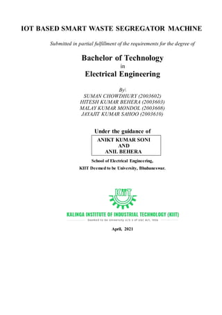
  • 1. IOT BASED SMART WASTE SEGREGATOR MACHINE Submitted in partial fulfillment of the requirements for the degree of Bachelor of Technology in Electrical Engineering By SUMAN CHOWDHURY (2003602) HITESH KUMAR BEHERA (2003603) MALAY KUMAR MONDOL (2003608) JAYAJIT KUMAR SAHOO (2003610) Under the guidance of School of Electrical Engineering, KIIT Deemed to be University, Bhubaneswar. April, 2021 ANIKT KUMAR SONI AND ANIL BEHERA
  • 2. I hereby declare that the thesis entitled “ Design and analysis of a multilevel inverter with boosting feature” submitted by me, for the award of the degree of Bachelor of Technology in Electrical Engineering to KIIT is a record of bonafide work carried out by me under the supervision of Prof. Tapas Roy. I further declare that the work reported in this thesis has not been submitted and will not be submitted, either in part or in full, for the award of any other degree or diploma in this institute or any other institute or university. Place : Bhubaneswar Date : Anirban Jana Anurag Sarkar Arup Kumar Saha Ishad Satyen Signature of the Candidate
  • 3. CERTIFICATE This is to certify that the thesis entitled “Design and Analysis of multileveel inverter with boosting feature” submitted by Anirban Jana, Anurag Sarkar, Arup kumar saha and Ishad satyen bearing roll no 1703085, 1703091, 1703152 and 1703148 School of Electrical Engineering, KIIT, Bhubaneswar, for the award of the degree of Bachelor of Technology in Electrical Engineering , is a record of bonafide work carried out by him under my supervision, as per the KIIT code of academic and research ethics. The contents of this report have not been submitted and will not be submitted either in part or in full, for the award of any other degree or diploma in this institute or any other institute or university. The thesis fulfills the requirements and regulations of the University and in my opinion meets the necessary standards for submission. Place : Bhubaneswar Date : The thesis is satisfactory / unsatisfactory Approved by Evaluation Committee Chairman, PMC Signature of the Guide
  • 4. ACKNOWLEDGEMENT We would like to express our deep sense of gratitude and appreciation to Prof. Tapas Roy for constant and valuable suggestion, guidance, encouragement and influence for bringing out of this project. We would further thankful to the Prof. (Dr.) B. K. Nayak, Dean, School of Electrical Engineering, all faculty members of school of Electrical Engineering and technical assistants of School of Electrical Engineering for their constant support.We would like to thank our project mates, for having many meaningful conversations and sharing those common thoughts together. Anirban Jana 1703085 Anuraag Sarkar 1703091 Arup Kumar Saha 1703152 Ishad Satyen 1703148
  • 5. Executive Summary In this work, the symmetrical and asymmetrical topologies of cascaded multi-level inverter (CMLI) are focused for a photo-voltaic (PV) system which is interconnected with grid through a cascaded H-Bridge (CHB) inverter using suitable modulation technique. The simulation is carried out using MATLAB/SIMULINK platform and total harmonic distortion (THD) level of both topologies is compared which decides the suitability for practical applications. Further the dynamic performance of a cascaded H-Bridge multilevel inverter (CHB-MLI) is described by using dual loop cascaded controller for addressing various issues. It consists of two loops i.e. outer loop and inner loop. The outer loop controller is a proportional-integral (PI) controller used as a voltage controller and inner loop controller is a proportional (P) controller used as a current controller. The steady state voltage i.e. constant output voltage with low THD is achieved with the help of the voltage controller, while the transient/dynamic performance is improved by using the current controller. The effectiveness of the controller has been tested on both linear and non-linear loads. The detailed step-by-step procedures for designing the control parameters of dual loop cascaded controller are given here. Finally, an optimal controller is developed for a grid connected PV system to control the power from PV system to the utility grid. The proposed controller ensures the unity power factor (UPF) operation as a result only active power is injected into the grid. The simulation is carried out using MATLAB/SIMULINK platform to evaluate the feasibility of the proposed controllers for controlling the grid current.
  • 6. CONTENTS Page No. Acknowledgement i Executive Summary ii Table of Contents iii List of Figures iv List of Tables vi Abbreviations viii Symbols and Notations ix S. No. Description Page No. CHAPTER 1 INTRODUCTION 1 1.1 Background 2 1.2 Classical MLIs 11 1.3 Research Motivation 15 1.4 Research Objective 15 1.5 Survey Papers on MLIs 16 CHAPTER 2 PROJECT DESCRIPTION AND GOALS 22 2.1 Goals 22 2.2 Aim 22 2.3 Function 22 2.4 Methodology 23 CHAPTER 3 TECHNICAL SPECIFICATION 27 3.1 Technical Specification of MLIs 27
  • 7. 3.2 Analysis of the proposed design 27 CHAPTER 4 DESIGN APPROACH AND DETAILS 29 4.1 Circuit Description 29 4.2 Design Approach 29 4.3 Codes and standards 33 4.4 Constraints, Alternatives and Trade-Offs 33 CHAPTER 5 SCHEDULE, TASKS AND MILESTONES 35 5.1 Project Development Stage 26 5.2 Road Map 26 CHAPTER 6 PROJECT DEMONSTRATION 36 6.1 Simulation Results 36 6.2 Experiment Analysis 40 6.3 Results and Discussion 44 CHAPTER 7 COST ANALYSIS 46 CHAPTER 8 SUMMARY 42 REFERENCES 44 APPENDIX A (PROGRAMS) 47 APPENDIX B (GANTT CHART) 55
  • 8. i List of Figures Figure No. Title Page No. 1.1 Configuration of Cascaded Multi-Level Inverter 8 1.2 Application areas of MLIs 11 1.3 Configuration of a Conventional Two-Level Inverter 13 1.4 Cascaded H- bridge MLI 13 2.1 Proposed CHB-MLI 17 3.1 Gate pulse generation 20 4.1 Block Diagram of PI Controller 23 4.2 Equivalent Circuit Diagram for Determination of Transfer Function 23 4.3 Principle of SPWM Technique 24 5.1 Road map 27 6.1 (a) Output Voltage (in Volt), (b) Load Current (in Amp) 29 6.2 (a) Voltage THD, (b) Current THD 29 6.3 Gate pulse generation 30
  • 9. ii List of Tables Table No. Title Page No. 1.1 Switching States of a 5-Level Inverter 8 1.2 Switching States of a 7-Level Inverter 9 1.3 Switching States of a 9-Level Inverter 10 1.4 Switching States of a 2-Level Inverter 13 2.1 Parameters for Design 19 4.1 IEEE-519 Standards for output voltage distortion 24 4.2 4.3 6.1 7.1 7.2 IEEE Standards for Current Distortion Limits comparison of new 9 level CHB-MLI with other 9 level topologies Filter and Controller Design Parameters for both Linear and Non-Linear Loads Cost estimation of components Cost Analysis for the measuring instruments and load 25 27 28 36 37
  • 10. iii List of Abbreviations CMLI Cascaded Multilevel Inverter PV Photo Voltaic CHB Cascaded H-Bridge THD Total Harmonic Distortion CHB-MLI Cascaded H-Bridge Multilevel Inverter V1 Input Voltage for Inverter 1 V2 Input Voltage for Inverter 2 Vd Magnitude of DC Input Voltage PI Proportional-Integral P Proportional I Integral UPF Unity Power Factor DG Distribution Generation MLI Multilevel Inverter PWM Pulse Width Modulation IGBT Insulated Gate Bipolar Transistor VLinv Inverter Input Voltage VAB Voltage across AB terminal UPS Uninterruptible Power Supply Kp Proportional Gain Ki Integral Gain fs Switching Frequency ma Modulation Index Vref Magnitude of Reference/Control Voltage Signal Vcar Magnitude of Carrier Voltage Signal SPWM Sinusoidal Pulse Width Modulation
  • 11. iv Symbols and Notations SL NO. SYMBOL Meaning 1 Ω Ohm 2 ° Degree 3 H Henry 4 F Farad 5 V Volt 6 A Ampere
  • 12. 5 CHAPTER 1 INTRODUCTION 1.1 Background Now-a-days most of the researchers have been focused on sources of renewable energy such as wind, solar and hydro power plant to produce energy due to the high availability of such energy in the world. A solar energy is considered as the best energy sources among all other renewable sources on the basis of economic scale of production. The solar energy industry in India is treated as fast growing plants. The government of Indian has already achieved the target of 20 GW for the year 2022 in 2018 [1]. The present installed capacity of solar power plant in India as of 30 Sept.19 is 31101 MW. The solar PV system has several advantages such as robust, freely available in nature and long life periods as compared to other energy sources. low maintenance and less production cost are the advantages so that the PV system is considered as the best candidature of the sources. Moreover, solar PV system can be interconnected with grid as a distribution generation (DG) system. Inverters are power electronic modules that are dedicated to the conversion of the electrical energy from DC power to AC power which is most used by today’s appliances. Inverters, in the family of power electronic converters are gaining more interest today because of the presence in most of renewable energy systems. With the advancement in semiconductor devices and control techniques, the power electronic converters are becoming affordable with better performances than before. The applications of DC/AC converters are one of the widest as they cover from small power applications such as portable devices, to high and medium power level applications such as electric vehicles and renewable energy systems. The applications require converters to produce better quality output voltage waveform. Further, the converter should be highly efficient, simple in control and low cost. For that, improvements are necessary for an efficient and better supply of power with high reliability and continuity. For different applications, different types of inverter topologies have been proposed in this thesis. Considering the output waveform, inverters are classified into [1]: • Two levels inverter • Three levels inverter • Multilevel inverters (MLI)
  • 13. 6 In medium and high power applications, the conventional three-level PWM inverters are becoming less popular because of their limitation to generate output voltage waveform with high magnitude and lesser harmonic distortion. This limitation of PWM inverters is addressed by increasing the switching frequencies. However, increasing switching frequencies create efficiency and electromagnetic interference (EMI) problems because of the increment of switching losses. To overcome these limitations, Multilevel Inverters (MLI) have been proposed that are made up of power switches and some passive components to achieve voltage of high magnitude that has lesser Total Harmonic Distortion (THD) and minimum voltage stress across switches [2]. Generally, the solar panel available in the market has the efficiency of approximately 15- 20%. The power efficiency and the quality of the output volage waveforms can be enhanced by using multilevel inverter (MLI). The solar PV system can be easily integrated with the utility grid with the help of the MLI [2]. This method of generation can be used for the medium to high power applications. In this work, the design and analysis of CMLI is carried out for the solar PV applications and it may or may not integrate with the utility grid [3]. 1.2 Overview of CHB MLIs The cascaded H-bridge (CHB) configurations are commonly used as the effective classic MLI topologies. These configurations comprises of two or more symmetrical single-phase H- Bridge modules which is represented in Figure 1.1. These MLIs can produce an ac voltage with required magnitude and frequency which has low total harmonic distortion (THD). These topologies are useful for the high rated power with less THD and low switching losses applications. The symmetric configuration of CHB MLIs can provide multiple number output voltage levels with multiple controllable semiconductor switches. The asymmetric topology of CHB MLIs with same number of switches can produce more output voltage levels as compared to its symmetrical topology [4]. If V1, V2 … Vn are the voltage supplied by the different PV panel to the indivisual H-n number of solar panels and the output voltage is given by (1). 𝑉𝐴𝐵 = 𝑉01 + 𝑉01 + ⋯+ 𝑉𝑜𝑛 (1)
  • 14. 7 S11 S13 + V1 - S14 S12 + V01 - S21 + S23 Output Voltag e (VAB) + V2 - S24 S22 V02 - S21 S23 + V2 - S24 S22 + V0n - Figure1.1: Configuration of Cascaded Multi-Level Inverter 1.2.1. CascadedMulti-LevelInverter (Symmetric) In symmetrical configuration [5] same magnitude of DC supply are applied to the inverter. 𝑉1 = 𝑉2 = ⋯ = 𝑉n = 𝑉d The number of voltage output levels (m) is evaluated by equatio (3). (2) 𝑚 = 2𝑛 + 1 (3) Where 𝑉𝑀 is maximum voltage produced. 𝑉𝑀 = 𝑛𝑉𝑑 (4) e.g. if n=3 i.e. 3 H-Bridges were connected in cascaded, then it produces 7 levels of output voltage [like -2Vd, -Vd, 0, Vd and 2Vd] with maximum value of voltage of 3Vd. Here, “0” and “1” are represented for “On” and “Off” states of controllable switches. TABLE 1.1: Switching States of a 5-Level Inverter Switches (VAB) Voltage Level Inverter 1 (V1= Vd) Inverter 2 (V2= Vd) S11 S1 2 S1 3 S14 S2 1 S22 S2 3 S2 4 2Vd 1 1 0 0 1 1 0 0 Vd 1 1 0 0 0 1 0 0 0 0 1 0 1 0 1 0 1 -Vd 0 0 1 1 0 1 0 1 -2Vd 0 0 1 1 0 1 1 1
  • 15. 8 1.2.2. Cascaded Multi-Level Inverter (Asymmetric) Due to application unequal magnitude of DC sources the configuration is known as asymmetrical configuration. DC voltage magnitudes of ratio of either 1:2:4 or 1:3:9 are applied. 1.2.3. Binary Asymmetrical MLI If the ratio is 1:2:4, then it is called binary asymmetric MLI [5]. The value of dc source will be evaluated by equation (5). 𝑉𝑛 = 2(𝑛−1) 𝑉𝑑 (5) The number of voltage output levels (m) is determined by equation(6). 𝑚 = 2(𝑛+1) − 1 (6) The maximum voltage produced is 𝑉𝑀 = (2𝑛 − 1)𝑉𝑑 (7) e.g. if n=3 i.e. only 3 H-Bridges were cascaded, to produce 15 levels of output voltage . Here, “0” and “1” are represented for “On” and “Off” states of controllable switches respectively. TABLE 1.2: 7-Level MLIs switching states Switches (VAB) Voltage Level Inverter 1 (V1= Vd) Inverter 2 (V2= 2Vd) S11 S12 S13 S14 S21 S22 S23 S24 3Vd 1 1 0 0 1 1 0 0 2Vd 0 1 0 1 1 1 0 0 Vd 1 1 0 0 0 1 0 1 0 0 1 1 1 0 1 1 1 -Vd 0 0 1 1 0 1 0 1 -2Vd 0 1 0 1 0 0 1 1 -3Vd 0 0 1 1 0 0 1 1
  • 16. 9 1.2.4. Trinary Asymmetrical Multi-Level Inverter If the ratio of DC voltage magnitudes is 1:3:9, then the configuration is called as trinary asymmetric MLI [5]. The dc source value can be evaluated as 𝑉𝑛 = 3(𝑛−1) 𝑉𝑑 (8) The number of voltage output levels (m) is calculated by equation(9). 𝑚 = 3𝑛 (9) The maximum voltage evaluated is represented as 𝑉 = 3𝑛−1 𝑉 (10) 𝑀 2 𝑑 e.g. if n=3 i.e. 3 H-Bridges in cascaded connection generates 27 levels of output voltage Here, “0” and “1” are represented for “On” and “Off” states of controllable switches. TABLE 1.3: Switching States of a 9-Level Inverter Switches (VAB) Voltage Level Inverter 1 (V1= Vd) Inverter 2 (V2= 3Vd) S11 S12 S13 S14 S21 S22 S23 S24 4Vd 1 1 0 0 1 1 0 0 3Vd 0 1 0 1 1 1 0 0 2Vd 0 0 1 1 1 1 0 0 Vd 1 1 0 0 0 1 0 1 0 0 1 0 1 0 1 0 1 -Vd 0 0 1 1 0 1 0 1 -2Vd 1 1 0 0 0 0 1 1 -3Vd 0 1 0 1 0 0 1 1 -4Vd 0 0 1 1 0 0 1 1 Merits of MLI over the conventional two level PWM inverters can be summarized as follow. ● MLI outputs are too close to sinusoidal waveform so that it has low THD. ●The dv/dt stress of MLI is too minimum compered to PWM inverters ● The stress in motor bearing, which use MLI control, is too low due to low common-mode voltage of MLIs: ● MLI works using either fundamental or high switching frequency modulation scheme
  • 17. 10 1.3. Mainapplication area of MLIs Different application area of MLIs are provided in Fig.1.5 [6]. Fig.1.2:Application areas of MLIs MLI has some demerits such as it requires many number of power switches, capacitors gate drivers, heat sinks, DC voltage sources which make it bulky, complex control circuit and costly. Therefore, a number of studies are being conducted to improve them, while some are seeking evolution of new structures, which have least number of power switches, capacitors, gate driver, and DC supply. Moreover, in forging inverters there is an absence of voltage boosting ability. So that the maximum output voltage is less than input voltage. To make the output voltage magnitude greater than the input voltage, it is common to use either DC-to-DC converter or inductor or transformer. However, these methods make the converter circuit more complex, bulky, and less efficient. So that to improve the forgoing shortcomings of MLIs Switched Capacitors (SC) is used in the MLI circuit in parallel/series fashion. The capacitor stores charge when it is connected in parallel with the supply voltage. The capacitor discharges its stored energy toward the load when it is connected in series with supply voltage. The number of capacitors in MLI is decided by the magnitude of the output voltage. In addition, SCMLI works either in fundamental switching frequency or in high switching frequency modulation strategies. One of the major advantages of SCMLI structure is that the structure does not require any complex control algorism to balance the capacitor voltages. However, the SCMLI has the limitation of large requirement of power switches and passive
  • 18. 11 A S1 S3 + Vi,inv Output Voltage - (V ) AB Solar Panel S4 S2 B components as the output voltage level enhances. In addition, SCMLI has higher switching stress and total standing voltage (TSV) To solve the forging shortcomings of SCMLs, this this project work develops a novel inverter structure, which reduces power device count considerably and boosts the output voltage. The structure of this proposed topology compared with recently developed structures. The effectiveness of the structure has been verified by MATLAB/Simulink. 1.3. ResearchMotivation A MLI is a power electronics converter which provides required AC output voltage of higher level using two or more DC voltages of lower level as an input. For designing such inverter circuit, semiconductor switches are used. As IGBT (Insulated Gate Bipolar Transistor) has high power rating, less conduction loss and less switching loss, it is used here as a switch. Mostly a two-level inverter is used in order to generate the AC voltage from DC voltage. The configuration of a two-level inverter is shown in Fig. 1. The MLI has advantages over conventional two-level inverter [4, 6] such as increasing in number of voltage level reduces the harmonic content and hence filter circuits required are reduced. Voltage stresses on the device is less than that of the overall operating voltage. Thus, a high voltage waveform can be obtained with switches having low rated voltage. It can be operated at both high switching frequency and fundamental frequency, but low switching frequency can cause reduce in switching loss with increase in efficiency. Also, grid without transformer can be interconnected with such renewable sources of energy. MLIs can draw low distorted input current compared to a two-level inverter. Figure 1. 3: Configuration of a Conventional Two-LevelInverter In Fig. 1 Vi,inv is the DC input voltage of the inverter taken from the solar panel. For the inverter circuit shown in Fig. 1, the switching states are given in Table 1.4. Here, “0” and “1” are represented for “On” and “Off” states of controllable switches.
  • 19. 12 TABLE 1.4: Switching States of a 2-Level Inverter Switches (VAB) VoltageLevels S1 S2 S3 S4 Vi,inv ON ON OFF OFF 0 ON OFF ON OFF OFF ON OFF ON -Vi,inv OFF OFF ON ON All the controllers referred to in section 1.2 offer good performance. Among these controllers PI controller is the most common used controller because it gives good result with easy design which makes the analysis simpler than others 1.4. Research Objective The ultimate goal of this dissertation is to develop an optimal controller so as to control the power from solar PV to the utility grid and to maintain the power factor at UPF. Another objective is to enhance the dynamic performance of the CHB-MLI by using dual loop cascaded controller so that it can be used for various applications like uninterruptible power supply (UPS) application and grid interconnection of solar PV system. The controller is designed in such a way that it can be used for both linear load as well as non-linear load. It is tested using MATLAB/SIMULINK platform with proper selection of controller parameters i.e. proportional gain (Kp) and integral gain (Ki). Further it has been interconnected with grid along with the loads. The effectiveness of the controller has been tested on both linear and non-linear loads. The detailed step-by-step procedures for designing the control parameters of dual-loop controller are given here. By the end of the thesis work, an optimal controller is developed for a grid connected system to control the power from PV system to the utility grid. The proposed controller ensures the UPF operation as a result only active power has been pumped into the grid. 1.5. Surveyed Papers on MLIs Some papers are related to the scope of renewable energy resources as given in [1]. In past years, a sigle bridge inverter is used to convert the DC voltage into an AC voltage, which is called as conventional two-level inverter and later MLI is used to convert the DC voltage to AC voltage, which gives better performance compared to conventional two-level inverter as given in [2], [4-9].
  • 20. 13 In some papers, various control strategies has been introduced for a grid connected inverter system to control over the grid current. In most of the cases iterative learning control, repetition dependent control and sliding mode control are suggested for pulse width modulation (PWM) technique for improving the dynamic performance of the system as given in [2-12], [13]. As the control scheme is voltage control, the output voltage waveform is sensitive to the variation of load. Some researchers has suggested PI controllers to be used for this control scheme as given in [14-16]. The paper [17] deals with simulation based comparison based on THD of the stand-alone CHB MLI. Different configurations of CHB MLI, such as symmetrical and asymmetrical configurations, are simulated by changing only the individual DC input voltages with the same model having only two bridge inverters cascaded. In symmetrical configuration the magnitudes of DC input voltages are same but in case of asymmetrical topology there are two-types of configurations are present such as binary asymmetric configuration and trinary asymmetric configuration as discussed in chapter 2. An asymmetric configuration of CHB- MLI with two bridge inverters cascaded can generate more levels of output voltage with less THD compare to other two configurations. In this paper, above mentioned all these configurations are modelled with the same two-bridge inverter cascaded module with a common pulse width modulation (PWM) technique using MATLAB/SIMULINK platform and their THD is compared for different switching frequency (fs) and different modulation index (ma). The paper [18] explores the control techniques for the stand-alone CHB MLI, which can be implemented for UPS Applications or can be interconnecting the solar PV system with the utility grid to transfer only active power from the solar to the grid at UPF. A UPS system is used for protecting the equipments like computers and medical devices from data loss caused by power failure interruption i.e. it can be used for any load either linear load or non-linear load. Hence, to improve the efficiency of UPS, an optimal dual loop cascaded controller is modelled in this paper and it is tested using MATLAB/SIMULINK platform. 1.6. Organization of Thesis This thesis work is organised with the following five chapters. Chapter 1 introduces about the thesis work which consists of introduction, literature review, motivation and objective. Chapter 2 is about analysis of CHB-MLI which contains different topologies of CHB inverter along with their switching states and their performance based comparisons are described.
  • 21. 14 Chapter 3 indicates the modulation techniques used for the switching of the inverter. It emphasizes different types of modulation techniques and the simulation of preferred modulation technique. In chapter 4, control of CHB-MLI for UPS application is discussed. In this section the UPS system, controller design for UPS and the simulation of the complete system for different loads are described. Chapter 5 elaborates the grid connected PV system. It includes the design of the controller for the grid current to maintain the power factor at UPF and it is tested using MATLAB/SIMULINK platform. Finally it concludes and the future scope of this thesis work is summarised in chapter 6.
  • 22. 15 CHAPTER 2 PROJECT DESCRIPTION AND GOALS 2.1. Goal i. To analyze the performance of noble CHB 9-level MLI ii. To develop a Hardware prototype of proposed CHB MLI to validate the feasibility of the design. 2.2. Aim i. Design of noble CHB 9-level MLI ii. Hardware prototype of proposed MLI. 2.3. Function: If the ratio of DC voltage magnitudes is 1:2:4, the configuration is called binary asymmetric MLI [5]. The value of each dc source can be determined by using (5). 𝑉𝑛 = 2(𝑛−1) 𝑉𝑑 (5) In binary asymmetric configuration the number of voltage output levels (m) is calculated by using (6). 𝑚 = 2(𝑛+1) − 1 (6) The maximum voltage generated by such arrangement shown in Fig. 1 is 𝑉𝑀 = (2𝑛 − 1)𝑉𝑑 (7) e.g. if n=2 i.e. only 2 H-Bridges were cascaded, then it generates 7 levels of output voltage [like -3Vd, -2Vd, -Vd, 0, Vd, 2Vd and 3Vd] with maximum voltage of 3Vd.
  • 23. 16 S11 S13 + V1 - S14 S12 + V01 - S21 + S23 Output Voltage (VAB) + V2 - S24 S22 V02 - S21 S23 + V2 - S24 S22 + V0n - Fig.2.1. Proposed CHB-MLI 2.4. Methodology The proposed research work has been performed in three following steps: mathematical modeling, simulation and hardware implementation. At first, a brief literature review was carried out to better understand the problems related with multilevel converters. A brief study was made on various types of MLI topologies by considering the application of the number of active and passive elements, proposed control schemes and switching techniques associated with the voltage balancing issue of the capacitor. In this step, existing models, controller, switching techniques and topologies have been simulated in Matlab/Simulink platform to list out the advantages and disadvantages of those reported technologies. The mathematical modeling of both proposed MLI topology and the existing topologies has been done to study the switching performance and design the advanced controllers. The developed topologies have been simulated in SPS with applied controllers to verify the good dynamic performance in stand-alone and grid-connected mode of operation. All possible transient modes such as load changing and AC or DC voltage variation have been investigated through the simulation to prevent any failure in hardware implementation.
  • 24. 17 Finally, proposed converters have been designed and made in the lab to test practically. Controllers and switching techniques have been implemented on dSpace1103 for rapid control prototyping.
  • 25. 18 CHAPTER 3 TECHNICAL SPECIFICATION The proposed 9 level structure is simulated using low frequency simulation strategy for 48V DC each supply. Simulation of proposed 13 level SCMLI is presented for different types of loads such as resistive load, inductive load, resistive-inductive load and dynamic loads In order to verify the feasibility of the proposed multilevel inverter topology and evaluate its performance with the corresponding modulation methods, the proposed 13-level multilevel inverter model is Hardware implemented for practical test. Hardware implementation and test of the proposed topology is practiced to verify the simulation results and the forgoing chapters’ analysis to get 50Hz output waveform. Table 3.1 Parameters for Design Item Name Quantity DC Sources 2 MOSFET Switch (IRF640) with heatsink 8 Gate Driver IC (IR2110) 8 Optocoupler (6N137) 16 Auxiliary circuits for gate driver 8 Isolated transformer 8 Wires - PCB printing for main inverter circuit 1 PCB for gate driver 8 Microcontroller and its auxiliary circuit 1
  • 26. 19 3.1. Analysis of the Proposed Circuit MOSFET IRF640, gate drive IC IR 2110 and electrolytic capacitor 3000µF are the main components are consumed for this experimental test practice. The main controller IC supply gate pulse for the MOSFET switches to fulfil the concept of Table .3.1 and the structures provided in Fig.3.1(a). Gate pulse generation Fig.3.1(b). Practical set-up of 13-level MLI Fig 3.1 and make the MOSFET switches ON and OFF. However, the controller IC output pulses are not enough to drive the MOSFETs gate [2]. Therefore, that amplification of the controller pulse is one of key function of gate driver circuit. To driver the power MOSFET at least 10V-15V is necessary so that gate driver circuit amplifies the main controller output pulse to this voltage level to be able to drive the power MOSFET. There is an optocoupler between the main controller IC and the gate driver IC (IR2110) to isolate from each other. The output of the gate driver is supplies between gate terminal of the MOSFET and the source. Here the technical specifically has been provided for hardware implementation.
  • 27. 20 CHAPTER 4 DESIGN APPROACH AND DETAILS 4.1. Circuit Description The input power is getting from various sources like solar PV system. The range of PV panel is Voltage 100V, Ampere=7.5A The energy is transferred from an unregulated line to a regulated sinusoidal output through a controlled pulses generated by SPWM techniques. Here the H-bridge cells are typically connected in dc input on their ac output side to achieve medium voltage operation and low harmonic distortion. The cascaded H- multilevel bridge inverter requires many isolated dc supplies, each of which feeds an H-bridge power cell. Inverter Its Convert Dc/Ac Ranges Capacitor For Reduce Noise Present In The Circuit  Finally, the inverted output voltage is given to stepup transformer to for load consume. 4.2. Operating Principle The principle of operation of nine level cascaded multilevel DC-link inverter is explained by explaining the operating principles of multilevel DC link voltage source and single phase full bridge inverter. To produce nine level AC output voltage Van the multilevel DC-link source is formed by connecting four H-bridge cells in series with each cell having a separate voltage source controlled by two switches S11 and S12 which will operate in a toggle fashion. The cell source is bypassed with Sak on and Sbk off, or adds to the DC link bus voltage by reversing the switches. The DC bus voltage Vbus is fed to the SPFB inverter. The switching signals shown in Figure 6(b) are given to the SPFB inverter in turn to alternate the
  • 28. 21 voltage polarity of the DC bus voltage Vbus for producing an AC output voltage Van of a stair case shape with (2n+1)=9 levels, whose voltages are - (V1+V2+........+ Vn) , -(V1+V2+.....Vn-1)......,-V2, -V1 ,0, V1, V2,......(V1+V2+....Vn-1), (V1+V2+....Vn). Where V1, V2.......Vn are voltages of cell sources. The desired AC output voltage Van of cascaded H-bridge is shown in the Figure 6(c). (1) The topology has voltage-boosting factor of 2, because from 3Vdc it generates 6Vdc. (2) It does not need any capacitor voltage balancing circuit. (3) The new topology applies three non-isolated symmetric DC voltage supply. 4.3. Controller Design Dual loop cascaded controller is suitable for MLI system for addressing issues. It consists of two loops i.e. outer loop and inner loop as shown in Fig. 11. In the outer loop PI controller is used as a voltage controller and in the inner loop P controller is used as a current controller. PI control system is the mixture of both P and I system. The PI controller is represented in time domain as given in (12) and in S-domain it is as given in (13). The block diagram of PI controller is shown in Fig. 13. The load voltage is sensed and compared with a reference signal for both linear and non-linear loads as shown in Fig. 14 and Fig. 18 respectively. The error voltage signal is sent to the PI controller, the output of which is taken as the reference signal for the current relative to the load current. Now, the present current error signal is fed back to P controller and this controller output is taken as reference/control signal for PWM technique. In time domain, 𝑢(𝑡) = 𝐾 𝑒(𝑡) + 𝐾 𝑡 𝑒(𝑟) 𝑑𝑟 (12) p i ∫𝑐=0 Where, 𝑒(𝑡) = 𝑆𝑉 − 𝑀𝑉 = Error Signal SV = Set Value i.e. Desired Value MV = Measured Value, which may different from SV In S domain i.e. in laplace form, 𝑢(𝑠) = [𝐾p + 𝐾i ]𝑒(𝑠) (13) 𝑠
  • 29. 22 G ( ) 𝑠 | 𝑖 Lf Io Vo,inv Cf Vo L O A D Figure 4.1: Block Diagram of PI Controller To achieve constant maximum output voltage even though any load change occurs, outer loop voltage controller is used and to get the sinusoidal current at the load side inner loop current controller is used. The transfer function [17, 18] for the load current (io) is given in (14) which is calculated from the Fig. 14. As the load current is dependent on load voltage and inverter output voltage hence, the transfer function is calculated as (14). Figure 4.2: Equivalent Circuit Diagram for Determination of Transfer Function For determination of transfer function consider Vo = 0, hence Cf gets opened G𝑜𝑙(𝑠)| = 𝑖𝑜 = 1 (14) 𝑖𝑜 𝑉𝑜=0 𝑉𝑜,𝑖𝑛𝑣 L𝐹s For PI controller, Cut-off frequency (𝑤𝑐𝑢𝑡_𝑜𝑓𝑓)<< Closed loop bandwidth (𝑤𝑐𝑙) 𝑤𝑐𝑢𝑡_𝑜𝑓𝑓 = 𝐾i 𝐾p => 𝐾i 𝐾p ≪ 𝑤𝑐𝑙 (15) G𝑜𝑙 (𝑠)| = (𝐾 + 𝐾i ) G𝑜𝑙(𝑠)| (16) 𝑠𝑦𝑠 𝑠=𝑗𝑤𝑐𝑙 p 𝑗𝑤𝑐𝑙 𝑖𝑜 𝑠=𝑗𝑤𝑐𝑙 From (15) and (16) it can be written as 𝑜𝑙 𝑠𝑦𝑠 𝑠=𝑗𝑤𝑐𝑙 = 𝐾pG𝑜𝑙(𝑠)| 𝑜 𝑠=𝑗𝑤𝑐𝑙 (17) 𝐾p = 1 |G𝑜𝑙 (𝑠)|𝑠=𝑗𝑤 and 𝐾i | = 𝐾𝑝𝑤𝑐𝑙 tan( −𝜋 −< 𝐺𝑜𝑙 (𝑠)|𝑠=𝑗𝑤 ) (18) 𝑖𝑜 𝑐𝑙 18 𝑖𝑜 𝑐𝑙 By using the formula given in (18), the calculated PI controller parameters for the outer loop controller are 𝐾p = 10 and 𝐾i = 100. Similarly, in addition to the transfer function, the p controller parameter for the inner loop has been calculated and found as 𝐾p = 0.2.
  • 30. 23 4.4. SPWM Technique The principle of SPWM technique is that, the reference signal is compared with the carrier signal and the switching pulses are generated as shown in Fig. 8 [6]. The formula for Modulation Index (ma) is given by (11). 𝑚𝑎 = 𝑉𝑅𝑒𝑓 𝑉𝑐𝑎𝑟 (11) Where, Vref = Magnitude of Reference/control Voltage i.e. Peak of Sine wave Vcar=Magnitude of Carrier Voltage i.e. Peak of Triangular wave 1 2 Figure 4.3: Principle of SPWM Technique 4.5. CODES AND STANDARDS As per the IEEE 519, harmonic voltage distortion on power systems 69 kV and below is limited to 5.0% total harmonic distortion (THD) with each individual harmonic limited to 3%. The current harmonic limits vary based on the short circuit strength of the system they are being injected into. Essentially, the more the system is able to handle harmonic currents, the more the customer is allowed to inject. The device used for verify the standard output based on standard ISO: 9000- Table : 4.1 IEEE-519 Standards for output voltage distortion Bus Voltage at PCC Individual Voltage Distortion (%) Total Voltage Distortion THD (%) Carrier Signal Reference Signal For VR ef ≥ Vcar Output is Logic 1 For VR ef ≤ Vcar Output is Logic 1
  • 31. 24 69 kV and below 3.0 5.0 69.001 kV through 161 kV 1.5 2.5 161.001 kV and above 1.0 1.5 Table: 4.2 IEEE Standards for Current Distortion Limits Maximum Harmonic Current Distortion in Percent of IL Individual Harmonic Order (Odd Harmonics) ISC/IL <11 11h<17 17h<23 23h<35 35h TDD <20* 4.0 2.0 1.5 0.6 0.3 5.0 20<50 7.0 3.5 2.5 1.0 0.5 8.0 50<100 10.0 4.5 4.0 1.5 0.7 12.0 100<1000 12.0 5.5 5.0 2.0 1.0 15.0 >1000 15.0 7.0 6.0 2.5 1.4 20.0 4.4. CONSTRAINTS, ALTERNATIVES AND TRADEOFFS 4.4.1. SystemConstraints: The proposed SCMLI have the following shortcoming or limitations i. Multiple DC source is required that can increase the cost of the system ii. Voltage stress of some switches are high iii. The capacitor has limited charging possibility 4.4.2. ALTERNATIVES AND TRADEOFFS Five other SCMLIs are used for this comparison study. Each of these topologies has its own weakness and strength. Table 4.2 shows a general comparison of the proposed voltage boosting SCMLIs with other SCMLIs in terms of equation for Number of switches, path, diodes, capacitors, drivers, DC supply and TSV. As shown in the Table 4.3 level proposed SCMLI is compared with five other SCMLIs in terms of number of DC voltage sources, Switches, drivers, diodes, capacitors, boosting factor, path (number of switches conducting to generate maximum voltage) and total max. Stress voltage (TSV). From the table it is possible to observe that for 13 level generation, the
  • 32. 25 number of switches, diodes, capacitors, drivers, TSV (PU), and path the proposed SCMLIs is minimum than any other five topologies. Table 4.3 comparison of new 9 level CHB-MLI with other 9 level topologies SCMLI presented NLevel Ndc Nsw Ndri Ndio Ncap TSV(pu) Boosting factor Npath [26] 13 2 16 16 2 4 5.6 2 7 [24] 13 2 20 16 0 6 5.3 3 6 [25] 13 3 21 21 12 6 4.5 1.5 9 [28] 13 2 14 11 14 2 5.33 2 5 [20] 13 3 18 18 24 3 7.5 4 9 Proposed one 13 3 13 11 0 1 4.2 2 5
  • 33. 26 CHAPTER 5 SCHEDULE, TASKS AND MILESTONES We decided on a few milestones for our project as we had to complete the project within a time frame of four months. 5.1 Project Development Process and Road Map Fig.5.1. Road map
  • 34. 27 CHAPTER 6 PROJECT DEMONSTRATION The proposed 13 level structure is simulated using low frequency simulation strategy for 48V DC each supply. Simulation of proposed 13 level SCMLI is presented for different types of loads such as resistive load, inductive load, resistive-inductive load and dynamic loads 6.1. Simulation Results The simulation is carried out using MATLAB/SIMULINK to verify the system as per our requirement, the simulation models for both linear load variation and non-liner load are shown in Fig. 15 and Fig. 19 respectively. For both linear load and non-linear load the same inner loop and outer loop controllers are used as shown in Fig. 15 and Fig. 19 with the same controller parameters as given in Table 7. The output voltage has seen by using the scope. THD is measured with the help of POWERGUI block in MATLAB/SIMULINK and the THD of output voltage for linear load and non-linear load is shown in Fig. 18 and in Fig. 22 respectively. Due to the inductive property of the load, the current has pure sinusoidal and 3A peak value as shown in the Fig.6.1 TABLE 6.1: Filter and Controller Design Parameters for both Linear and Non-Linear Loads DesignParameters Symbol Numerical Value InverterInput Voltage Vi,inv 100 Volt AC ReferenceVoltage VRef 80 Volt FilterComponents (LinearandNon-Linear Load) Lf 20 mH Cf 100 µF LinearLoadParameters R1 10Ω R2 10Ω Non-LinearLoadParameters R1 1 Ω R2 4 Ω C 100 µF Loop:PI Controller Kp 10 Ki 100
  • 35. 28 From the waveform, capacitor maximum voltage is 143.6V whereas min. voltage is 138.7V. In addition, the ripple voltages (ΔVC) is found to be 4.9V. As shown in Fig 5.4 (a) and (b) the 285.9V and 2.98A are the peak value of fundamental output voltage and current respectively. Also 6.46% and 0.96% are voltage THD and current THD of the simulation results respectively. For resistive load (R L = 96Ω), output current and voltage are in phase and are 2.89 and 289V are peak value respectively as it is shown in Fig. 6.5. The waveform of inductive load as shown in Fig5.6 voltage and current are out of phase by 90 degrees to each other.Fig.6.7 indicates the dynamic load waveform of current and voltage. As it can be seen from the Fig.6.7 the shape of waveform does not change however, the magnitude of the waveform changes with the load change. Fig.6.1 (a) Output Voltage (in Volt), (b) Load Current (in Amp) Fig.6.2 (a) Voltage THD, (b) Current THD
  • 36. 29 6.2. Experimental Analysis MOSFET IRF640, gate drive IC IR 2110 and electrolytic capacitor 3000µF are the main components are consumed for this experimental test practice. The main controller IC supply gate pulse for the MOSFET switches to fulfil the concept of Table 1.1 and the structures provided in Fig.6.3(a). Gate pulse generation Fig.6.3(b). Practical set-up of for the experiment Fig.2.1 and make the MOSFET switches ON and OFF. However, the controller IC output pulses are not enough to drive the MOSFETs gate [2]. Therefore, that amplification of the controller pulse is one of key function of gate driver circuit. To driver the power MOSFET at least 10V-15V is necessary so that gate driver circuit amplifies the main controller output pulse to this voltage level to be able to drive the power MOSFET. There is an optocoupler between the main controller IC and the gate driver IC (IR2110) to isolate from each other. The output of the gate driver is supplies between gate terminal of the MOSFET and the source. The gate pulse procedure and practical set-up are shown in 6.8 a) and (b). In this experiment of the new topology only 13 level module is implemented. The experimental hardware implementation test is conducted for 13 level 15V DC voltage for more practical realization since one solarunit PV output voltage is 12Vor 24v DC. The
  • 37. 30 Proposed SCMLI is tested for different types of loads such as resistive load, inductive load, resistive- inductive load and dynamic load to verify the practical performance of the topology. The load values for which the test is conducted; resistive load is 100Ω and inductive load 150mH. Fig.6.9 Vo (t) and Io(t) for 10V DC From the above Fig.6.2. it is possible to observe that at an input voltages 10VDC the load voltage has 13 level and Vpeak = 60V peak AC. Moreover, the peak current is 0.6A similar to that of the theoretical explanation.Fig 13.3. (a) Shows that for VDC = 15V input and resistive load (RL) =100Ω, peak output voltage (Vomax) = 90V and the peak output current (Iomax) is also 0.9A AC. Fig 6.3. (b) as well indicate for input 15VDC, the capacitor charged to 45V peak. From Fig.6.4. it can be possible to see that for input 15VDC, the peak to peak capacitor ripple voltage is about 1.56V. Fig.6.5. show that input current varies with charging and discharging of capacitor. But charging and discharging of capacitor doesn’t have visible effect on output voltage and current (a) (b) Fig. 6.10 Voltage, Current output waveform and (b) capacitor DC voltage
  • 38. 31 (a) (b) Fig.6.11. capacitor ripple voltage (a) Multi Cycle (b) One Cycle (a) (b) Fig.6.12. Input current and capacitor waveform (a) for iin1(t) and iin2(t) (b) iin3(t) and ic(t)and Vo Fig.6.6. indicates the stress voltage across switches S1 , S2 ,S3,S4 and S5 which is 45VDCmaximum or 3VDC. We can see that S1 and S2are complementary to each other i.e. when S1 is made ON S2 will be OFF and vice versa. Fig.6.7 shows the stress voltage across Switches S6, S7, S8 and S9. It is possible to observe the Fig.6.7 switches S6and S7 and S8 and S9 are complementary to each other. From the maximum stress voltage across S6, S7, S8 and S9is about 45V which is 3Vdc. Fig. 13.8 shows that switches S10and S11 are complementary to each other; that is when switch S10 is made ON, switch S11 will be OFF. Moreover, the maximum stress voltage across the switches is 45V as we can see from the Fig.6.13.
  • 39. 32 (a) (b) Fig.6.13. Stress voltage across :(a) S1 and S2 (b) S3, S4 and S5 and Vo(t) (a) (b) Fig. 6.14. Stress voltage across of (a) S6 and S7 (b) S8and S9 Fig 6.14 Stress voltage across switch S10and S11 The maximum stress current through the switches S1, S10 , S4 and S7for resistive load RL=100Ω as shown in Fig.6.9 (a) , (b) and is 0.8A. From Fig.6.14 (b) and (c) we can see that maximum current stress through switches S3, S5 and S9 is 3.7A. This 3.7A stress
  • 40. 33 current across switches S3, S5and S9 is due to charging and discharging of the capacitor. Therefore, the maximum switch stress occurs across switches during capacitor charging. (a) (b) (c) Fig.6.15 current stress across (a) S1 and S10(b) S3, S4 and S5 (c) S7 and S9 The test also conducted for R-L load to observe the new topology feasibility for different types of loads. Fig 6.15. (a) show us the output current and voltage for L =50mH, and RL= 50Ω. Load. It possible to see that phase difference between current and voltage which indicates as the load has more inductive property. Similarly, Fig.6.16 (b) is for output current and voltage for R-L load. In this case the phase difference is too small to say the load is more resistive (L=50mH, RL=100Ω) Fig. 6.17 indicates the output voltage & current for pure inductive load with RL = 10Ω and L = 150mH & possible see 90- degree phase difference
  • 41. 34 (a) (b) Fig.6.16 output voltage waveform for R-L load (a) more inductive load (b) more resistive load . Fig.6.17 pure inductive load
  • 42. 35 CHAPTER 7 COST ANALYSIS This chapter describes the cost analysis of the project work. The hardware laboratory prototype has been developed within 500W. The cost of the inverter depends on the power rating of the proposed inverter. The inverter requires 3 DC sources, 13 switches and their attached heat- sinks, gate driver circuits, isolated transformers, switched capacitor, optocouplers. The gate pulses for the inverter has been realized by low cost microcontrollers. 7.1. Cost Analysis The detail cost of the project in terms of $ and Rs are shown in Table 7.1. Fig.7.1. Cost Analysis for the proposed Inverter circuit Table: 7.1 Cost estimation of components Item Name Quantity Cost per item in $(Rs) Total cost in $(Rs) DC Sources 3 $628.3(Rs.46000) $1884.9(Rs.138000) MOSFET Switch (IRF640) with heatsink 13 $1.707 (Rs. 125) $18.78(Rs.1375) Gate Driver IC (IR2110) 11 $1.23 (Rs. 90) $13.53(Rs.990) Optocoupler (6N137) 22 $0.41 (Rs. 30) $9.02(Rs.660) Auxiliary circuits for gate driver 11 $2.73 (Rs. 200) $30.03(Rs.2200) Isolated transformer 11 $3.41 (Rs. 250) $37.51(Rs.2750) Wires - $3.00 (Rs. 220) $3.00(Rs.220)
  • 43. 36 PCB printing for main inverter circuit 1 $10.92 (Rs. 800) $10.92 (Rs. 800) PCB for gate driver 11 $4.09 (Rs. 300) $44.99(Rs.3300) Microcontroller and its auxiliary circuit 1 $19.12 (Rs. 1400) $19.12 (Rs. 1400) Total cost of the proposed inverter with out measuring instruments and load $2071.8(Rs.1,51,676) Along with the above cost of the inverter prototype, the set-up associated with the measuring instruments such as isolated oscilloscope, voltage probes, current probes, load inductance and resistance, digital voltmeter. Furthermore, the whole soldering process has been done in the research lab. So there is the cost of soldering station, solder wires etc. The summarize cost involved in the above mentioned items are shown in below Table. Table.7.2. 0 Item Name Quantity Cost per item in $(Rs) Total cost in $(Rs) 4 channel Isolated Oscilloscope 1 $8195.3(Rs.600000) $8195.3(Rs.600000) Isolated voltage probes 4 $61.46 (Rs. 4500) $245.84(Rs.18000) Isolated current probes 3 $273.18 (Rs. 20000) $819.54(Rs.60000) Soldering station, and accessories 1 $75.12 (Rs. 5500) $75.12 (Rs. 5500) Load and accessories 1 $71.02 (Rs. 5200) $71.02 (Rs. 5200) Total cost of the measuring instruments and load $9406.8(Rs.6,88,673)
  • 44. 1 CHAPTER 8 SUMMARY 2.1. Societal Impact The project focuses on the modeling and simulation study of a modified SCMLI structure. The structure uses 3 sources and 1 capacitor to realize 13 output voltage level. The societal impact of this project work is as follows: In recent years, one of the major challenges of mankind is the global warming. To reduce the global warming, the prime solution is the production of clean energy from renewable sources such as PV, hydrogen gas, and fuel cells. However, to harvest the energy from these sources, an efficient, cost effective conversion system is required. In this conversion system, one of the major elements is the inverter system. The proposed inverter can realize high quality output voltage waveform with boosting factor of 2 that means can realize double voltage at the output from a source. This boosting feature of the proposed inverter can reduce the size of the inverter with respect to the conventional inverter. Furthermore, the inverter needs lower switches and single capacitor 13 level output voltage that is significantly lower than other inverters. This reduce part count minimizes the losses and improve the efficiency of the inverter as well as the overall conversion system. So one of the important societal impact of proposed inverter is the reduction of carbon emission by improving the system efficiency and reducing the cost of the inverter structure. 2.2. Conclusion From the forging chapters it is possible to observe that the proposed topology in this thesis having SC as a basic unit can produce double output voltage compared to input voltage with
  • 45. 2 minimum number of components. Some other merits of this project work are: All the sources can be added to each other and with the capacitor to supply higher output voltage. Therefore, that output voltage is higher than the input voltage.The topology proposed in this thesis has no H – bridge. The proposed topology has three non-isolated DC sources.Simulation of the proposed topology is conducted for resistive, resistive-inductive, inductive, and dynamic loads to see the feasibility of the topology for different loads. 2.3. Future works  Hardware implementation of the proposed SCMLI structure  Integration of PV module with the proposed inverter Reference [1] B. R. Singh and O. Singh, “Future Scope of Solar Energy in India.,” SAMRIDDHI A J. Phys. Sci. Eng. Technol., vol. 8, no. 1, 2016. [2] J. Rodriguez, S. Bernet, B. Wu, J. O. Pontt, and S. Kouro, “Multilevel voltage- source-converter topologies for industrial medium-voltage drives,” IEEE Trans. Ind. Electron., vol. 54, no. 6, pp. 2930–2945, Dec. 2007. [3] L. G. Franquelo; J. Rodriguez, J. I. Leon, S. Kouro, R. Portillo, and M. A. M. Prats, “The age of multilevel converters arrives,” IEEE Ind.Electron. Mag., vol. 2, no. 2, pp. 28–39, Jun. 2008. [4] G. Jayapalan and B. Edward, “Comparison of Symmetrical and Asymmetrical Cascaded H-Bridge Multilevel Inverter Using Pulse Width Modulation,” IJPAM, Vol. 118, no. 17, February, 2018. [5] M. Calais, V. G. Agelidis, “Multilevel Converter for Single-Phase Grid Connected Photo Voltaic Systems – An Overview”, Proc. IEEE Int. Symp. Industrial Electronics, 1998, Vol. 1. [6] A. Sinha, M. K. Das, and K. C. Jana, “Control of asymmetrical cascaded multilevel inverter for a grid-connected photovoltaic system,” IET Renew.
  • 46. 3 Power Gener., vol. 13, no. 9, pp. 1456–1465, 2019. [7] A. Prayag, S. Bodkhe, and G. H. Raisoni, “A Comparative Study of Symmetrical and Asymmetrical Cascaded H Bridge Multilevel Inverter Topology for Industrial Drive,” IRJET, pp. 1931–1936, 2018. [8] M. H. Rashid, “Power Electronic Circuits, Devices and Application,” 3rd Edition. Pearson Prentice Hall, 2004. [9] J. G. Shankar and J. Belwin Edward, "A 15-level asymmetric cascaded H bridge multilevel inverter with less number of switches for photo voltaic system," 2016 International Conference on Circuit, Power and Computing Technologies (ICCPCT), Nagercoil, 2016, pp. 1-10. [10] A. K. Ranjan, D. V. Bhaskar, and N. Parida, “Analysis and simulation of cascaded H-Bridge multi level inverter using level-shift PWM technique,” IEEE Int. Conf. Circuit, Power Comput. Technol. ICCPCT 2015, vol. 1, pp. 1– 5, 2015. [11] N. Bhargava, S. Gupta, and S. P. Phulambrikar, “Analysis of Asymmetrical Cascaded 7 Level and 9 Level Multilevel Inverter Design for Asynchronous Motor,” IJERT, vol. 3, no. 8, pp. 499–504, 2014. [12] O. Kukrer, H. Komurcugil, and A. Doganalp, “A three-level hysteresis function approach to the sliding-mode control of single-phase UPS inverters,” IEEE Trans. Ind. Electron., vol. 56, no. 9, pp. 3477–3486, 2009. [13] I. J. Nagrath, M. Gopal, “Control Systems Engineering,” 5th Edition, New Age International Publishers. [14] P. K. Sahu and S. Maity, "Dynamic performance enhancement of voltage source inverter by constant-frequency hysteretic current controller," Proceedings of the 2014 IEEE Students' Technology Symposium, Kharagpur, 2014, pp. 193-198. [15] M. Tariq, Md. Meeraj, A. Azeem, B. Chokkalingam “Evaluation of Level- Shifted and Phase-Shifted PWM Schemes for Seven Level Single-Phase Packed U Cell Inverter,” CPSS Trans. Power Electron. Appl., vol. 3, no. 3, pp. 232–242, 2018. [16] F. Liu, Y. Zhou, S. Duan, J. Yin, B. Liu, and F. Liu, "Parameter Design of a Two-Current-Loop Controller Used in a Grid-Connected Inverter System With LCL Filter," in IEEE Transactions on Industrial Electronics, vol. 56, no. 11, pp. 4483-4491, Nov. 2009.
  • 47. 4 [17] M. H. Mahlooji, H. R. Mohammadi, and M. Rahimi, “A review on modeling and control of grid-connected photovoltaic inverters with LCL filter,” Renew. Sustain. Energy Rev., vol. 81, no. August 2017, pp. 563–578, 2018. [18] B. Pal, P. K. Sahu and S. Mohapatra, "A review on feedback current control techniques of grid-connected PV inverter system with LCL filter," 2018 Technologies for Smart-City Energy Security and Power (ICSESP), Bhubaneswar, 2018, pp. 1-6. [19] A. K. Acharya, P. K. Sahu, Kundan Kumar and KVVSR Chowdary, "Simulation and Analysis of Single-Phase Cascaded H-Bridge Multi-Level Inverter for Solar PV Application," International Conference on Emerging Trends for Smart Grid Automation and Industry 4.0 (ICETSGAI 4.0), Dec- 2019, pp. 1-10. [20] A. K. Acharya, P. K. Sahu, Kundan Kumar and KVVSR Chowdary, "Enhancement of Dynamic Performance of a Single Phase Cascaded H-Bridge Multilevel Inverter Using Closed Loop Controllers," IEEE International Conference on Computational Intelligence for Smart Power System and Sustainable Energy (CISPSSE-2020), May-2020, pp. 1-5.
  • 48. 5 Capstone Project Project Title Design and analysis of a multilevel inverter with boosting feature Team Members (Names and Reg Nos.) Anirban Jana , Anurag Sarkar, Arup Kumar Saha and Ishan Satyen Faculty Guide Prof. Tapas Roy Semester/ Year VIII / IV year Project Abstract (not more than 200 words) Multilevel Inverter (MLI) is one of the main component associated with energy conversion systems. Highly efficient, compact and lower weight inverter structure has a prominent demand in different industrial applications such as motor drives, uninterrupted power supplies (UPS), induction heating, electric vehicles etc.. Switched capacitor multilevel inverters (SCMLIs) can overcome the different limitations of conventional MLIs. They can balance the capacitor voltages inherently. They have the boosting feature that is essential for PV applications. Importantly SCMLIs require a lower count of DC sources as compared to cascaded MLI that reduces the cost of the inverter for realizing same quality of output voltage. In this project work, a novel MLI structure using switched capacitor principle has been proposed. The structure needs lower components such as power switches, capacitors as compared to the recently developed SCMLIs. Extensive simulation study has been presented on proposed 13 level structure to verify its performances. Project Title Design and analysis of a multilevel inverter with boosting feature List codes and standards that significantly affect your project. IEEE 519 and ISO: 9000 List at least two significant realistic design constraints that are applied to your project. The proposed SCMLI design constraints are as follows: i. 3 number of DC source is required that can increase the cost of the system
  • 49. 6 ii. Voltage stress of some switches are high iii. The capacitor has limited charging possibility Briefly explain two significant trade-offs considered in your design, including options considered and the solution chosen The proposed 13 level proposed SCMLI is compared with five other SCMLIs in terms of number of DC voltage sources, Switches, drivers, diodes, capacitors, boosting factor, path (number of switches conducting to generate maximum voltage) and total max. Stress voltage (TSV). It is designed in such a way that the number of switches, diodes, capacitors, drivers, TSV (PU), and path the proposed SCMLI is minimum than any other five topologies. Describe the computing aspects, if any, of your project. Specifically identifying hardware-software trade-offs, interfaces, and/or interactions First of all, the idea of the proposed gets confirmed after the rigorous literature survey to have the advantages ofminimum number of switches, diodes,capacitors, drivers, TSV (PU) . For detail analysis, the MATLAB/Simulink has been used and for validation the experimental setup has been created. Background Knowledge from the course 3rd semester Analog Circuit: EC 2015 3rd Semester Network Analysis EE 2003 5th Semester: Power Electronics EE 3005