Download as PDF, PPTX

![Thermal Vias
effective vertical thermal conductivity
(0,8mm FR4 board, 25µm Cu plating in vias)
120.0
100.0
via diameter
100.0E-6
W/mK]
80.0 200.0E-6
thermal conductivity [W
300.0E 6
300 0E-6
400.0E-6
500.0E-6
60.0 700.0E-6
1.0E-3
40.0
20.0
20 0
-
000 0 0
000.0E+0 200.0E-6
00 0 6 400.0E-6
00 0 6 600 0 6
600.0E-6 800 0 6
800.0E-6 1.0E-3
0 3
via pitch [m]
LED Fundamentals | External Thermal Resistance - Substrates| Page 5](https://image.slidesharecdn.com/osram-osledfundamentalsexternalthermalresistance-substrates1-3-2012-121218091358-phpapp01/85/External-Thermal-Resistance-Substrates-LED-Fundamentals-5-320.jpg)


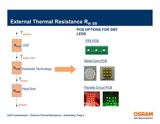
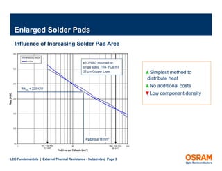
The document discusses the fundamentals of external thermal resistance in relation to LED substrates, detailing various substrate technologies, including FR4 PCB and metal core PCB, and their thermal conductivity characteristics. It also highlights design considerations such as enlarged solder pads and thermal vias to improve heat transfer and manage junction temperatures. Furthermore, it emphasizes the impact of these factors on LED performance and the importance of careful design to avoid potential issues.