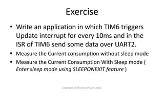
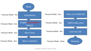
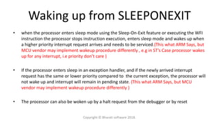
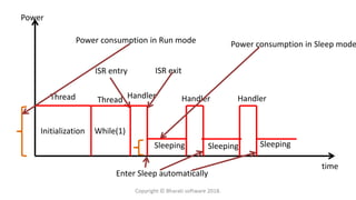
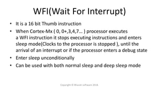
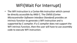
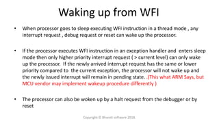
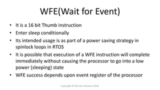
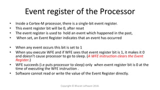
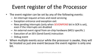
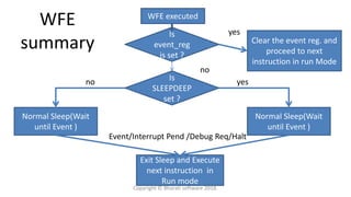
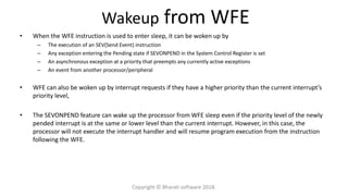
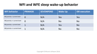
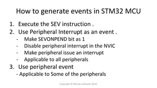
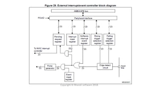
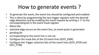
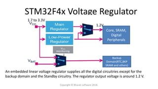
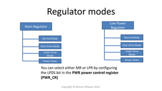
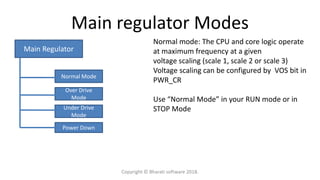
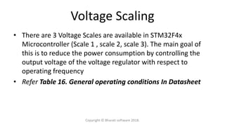
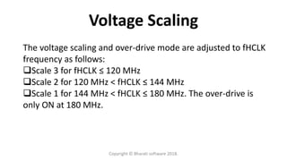
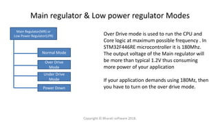
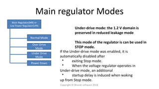
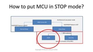
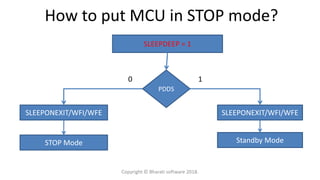
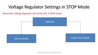
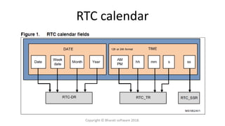
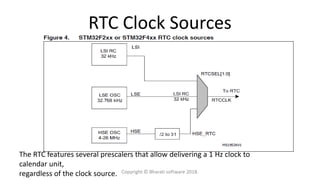
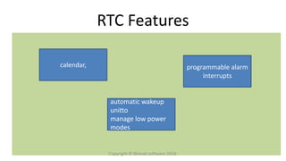
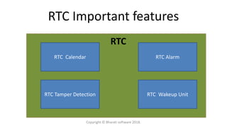
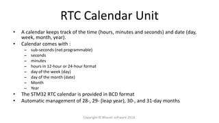
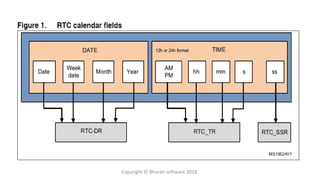
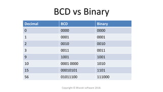
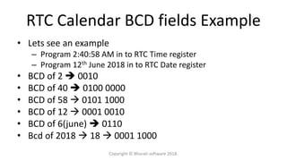
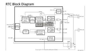
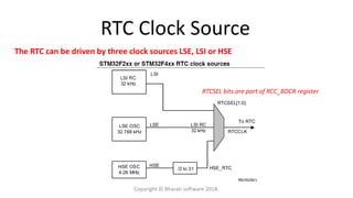
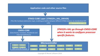
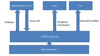
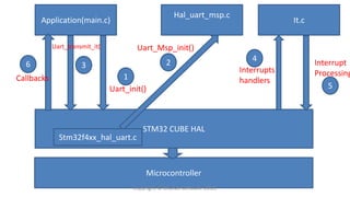
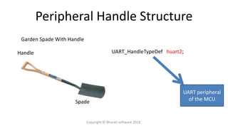
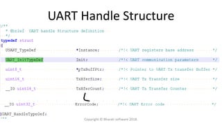
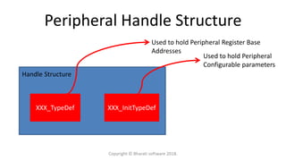
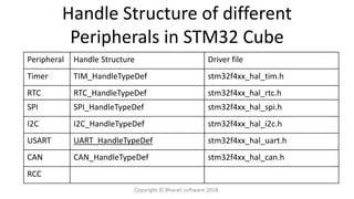
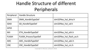
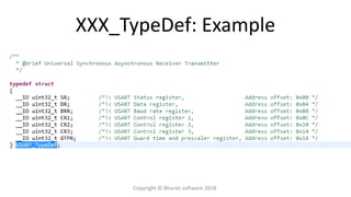
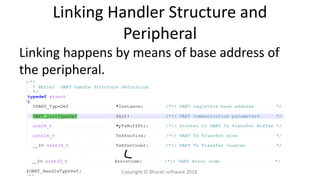
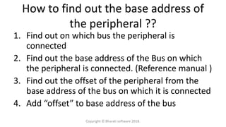
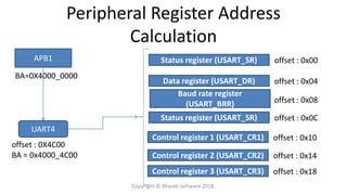
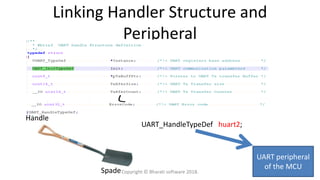
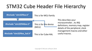
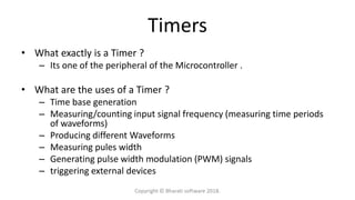
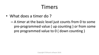
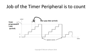
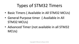
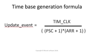
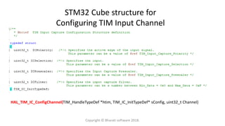
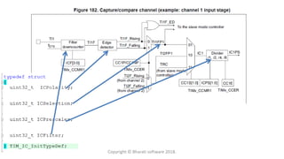
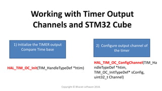
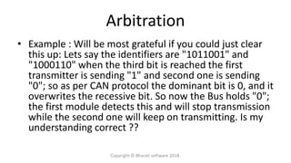
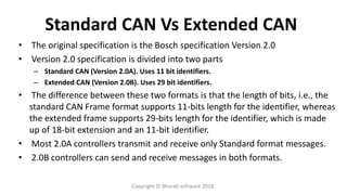
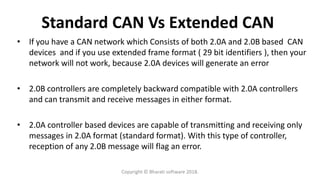
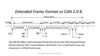
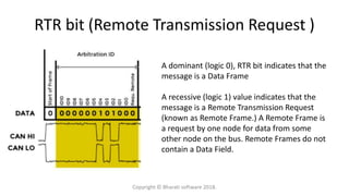
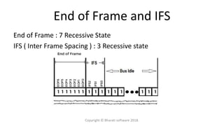
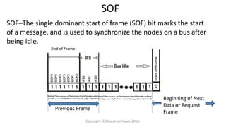
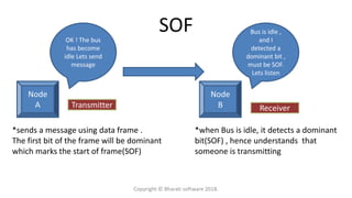
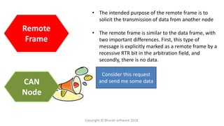
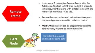
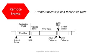
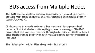
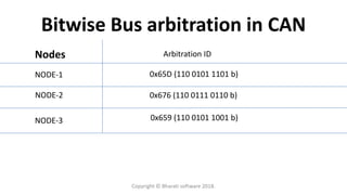
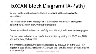
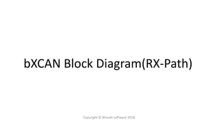
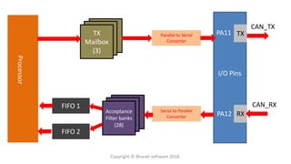
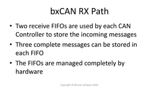
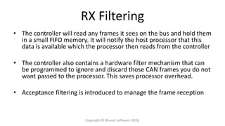
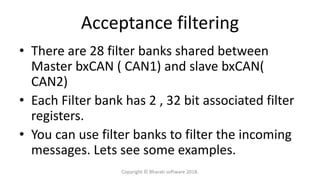
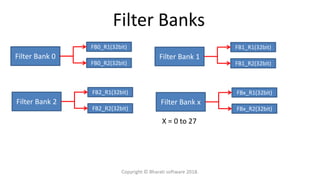
This document provides an overview of the Fastbit Embedded Brain Academy's online training on microcontrollers, including setup procedures and relevant configurations for STM32 microcontrollers using HAL (Hardware Abstraction Layer). It discusses timer functionality, initialization, and interrupt handling, culminating in practical exercises for UART and timer usage. Key elements include the structure of peripherals, register management, and the integration of HAL for effective programming in embedded systems.


![bxCAN Tx and STM32 Cube
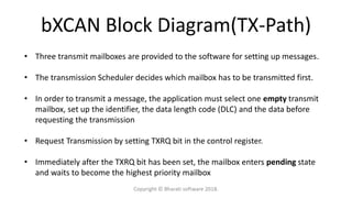
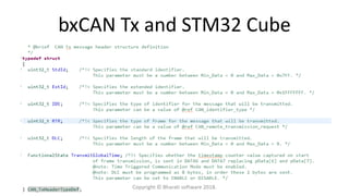
HAL_CAN_AddTxMessage(CAN_HandleTypeDef *hcan,
CAN_TxHeaderTypeDef *pHeader,
uint8_t aData[], uint32_t *pTxMailbox)
Copyright © Bharati software 2018.](https://image.slidesharecdn.com/mcu2-190826062428/85/Mastering-Microcontroller-TIMERS-PWM-CAN-RTC-LOW-POWER-165-320.jpg)

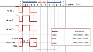
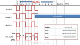
![31 30 29 28 27 26 25 24 23 22 21 20 19 18 17 16 15 14 13 12 11 10 9 8 7 6 5 4 3 2 1 0
0
R
T
R
ID
EEXID[4:0]EXID[12:5]EXID[17:13]STID[10:3] STID[2:0]
31 30 29 28 27 26 25 24 23 22 21 20 19 18 17 16 15 14 13 12 11 10 9 8 7 6 5 4 3 2 1 0
31 30 29 28 27 26 25 24 23 22 21 20 19 18 17 16 15 14 13 12 11 10 9 8 7 6 5 4 3 2 1 0
Identifier Register
Mask Register
fields Mapping
Filter Bank 0
FB0_R1(32bit)
FB0_R2(32bit)
Copyright © Bharati software 2018.](https://image.slidesharecdn.com/mcu2-190826062428/85/Mastering-Microcontroller-TIMERS-PWM-CAN-RTC-LOW-POWER-173-320.jpg)
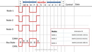
![31 30 29 28 27 26 25 24 23 22 21 20 19 18 17 16 15 14 13 12 11 10 9 8 7 6 5 4 3 2 1 0
0
R
T
R
ID
EEXID[4:0]EXID[12:5]EXID[17:13]STID[10:3] STID[2:0]
31 30 29 28 27 26 25 24 23 22 21 20 19 18 17 16 15 14 13 12 11 10 9 8 7 6 5 4 3 2 1 0
31 30 29 28 27 26 25 24 23 22 21 20 19 18 17 16 15 14 13 12 11 10 9 8 7 6 5 4 3 2 1 0
Identifier Register-1
Identifier Register-2
fields Mapping
Filter Bank 0
FB0_R1(32bit)
FB0_R2(32bit)
Copyright © Bharati software 2018.](https://image.slidesharecdn.com/mcu2-190826062428/85/Mastering-Microcontroller-TIMERS-PWM-CAN-RTC-LOW-POWER-174-320.jpg)
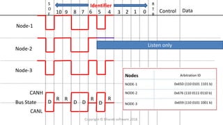
![31 30 29 28 27 26 25 24 23 22 21 20 19 18 17 16 15 14 13 12 11 10 9 8 7 6 5 4 3 2 1 0
0
R
T
R
ID
EEXID[4:0]EXID[12:5]EXID[17:13]STID[10:3] STID[2:0]
31 30 29 28 27 26 25 24 23 22 21 20 19 18 17 16 15 14 13 12 11 10 9 8 7 6 5 4 3 2 1 0
31 30 29 28 27 26 25 24 23 22 21 20 19 18 17 16 15 14 13 12 11 10 9 8 7 6 5 4 3 2 1 0
Identifier Register
Mask Register
fields Mapping
Filter Bank 0
FB0_R1(32bit)
FB0_R2(32bit)
FilterIdHigh FilterIdLow
FilterMaskIdHigh FilterMaskIdLow
Copyright © Bharati software 2018.](https://image.slidesharecdn.com/mcu2-190826062428/85/Mastering-Microcontroller-TIMERS-PWM-CAN-RTC-LOW-POWER-187-320.jpg)