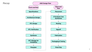
● Placement: Placementis the process of automatically assigning correct
position to standard cells inside core area with no overlapping. By
global placement, standard cells will placed be inside core area roughly.
By the detailed placement the standard cells will place in site rows
(legalize placement). After placement stage we check for congestion
and Timing we also reduce it.
● CTS (clock tree synthesis): In this stage we build the clock tree by using
inverters and buffers. In the chip clock signal is essential to the flip
flops. To supply the clock signal from clock source we built the clock
tree. It is the process of balancing the clock skew and minimizing
insertion delay in order to meet timing and power.
3
Physical Design Terminology
4.
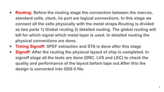
● Routing: Beforethe routing stage the connection between the macros,
standard cells, clock, i/o port are logical connections. In this stage we
connect all the cells physically with the metal straps.Routing is divided
as two parts 1) Global routing 2) detailed routing. The global routing will
tell for which signal which metal layer is used. In detailed routing the
physical connections are done.
● Timing Signoff: SPEF extraction and STA is done after this stage
● Signoff: After the routing the physical layout of chip is completed. In
signoff stage all the tests are done (DRC, LVS and LEC) to check the
quality and performance of the layout before tape out.After this the
design is converted into GDS II file.
4
5.
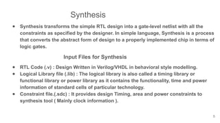
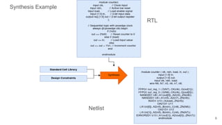
Synthesis
● Synthesis transformsthe simple RTL design into a gate-level netlist with all the
constraints as specified by the designer. In simple language, Synthesis is a process
that converts the abstract form of design to a properly implemented chip in terms of
logic gates.
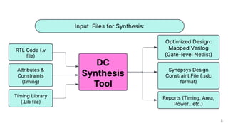
Input Files for Synthesis
● RTL Code (.v) : Design Written in Verilog/VHDL in behavioral style modelling.
● Logical Library file (.lib) : The logical library is also called a timing library or
functional library or power library as it contains the functionality, time and power
information of standard cells of particular technology.
● Constraint file.(.sdc) : It provides design Timing, area and power constraints to
synthesis tool ( Mainly clock information ).
5
6.
Synthesis
● Synthesis transformsthe simple RTL design into a gate-level netlist
with all the constraints as specified by the designer. In simple language,
Synthesis is a process that converts the abstract form of design to a
properly implemented chip in terms of logic gates.
6
7.
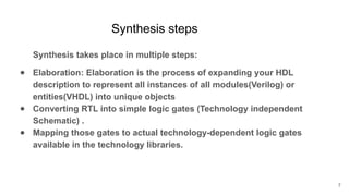
Synthesis steps
Synthesis takesplace in multiple steps:
● Elaboration: Elaboration is the process of expanding your HDL
description to represent all instances of all modules(Verilog) or
entities(VHDL) into unique objects
● Converting RTL into simple logic gates (Technology independent
Schematic) .
● Mapping those gates to actual technology-dependent logic gates
available in the technology libraries.
7
Output from Synthesistool:
● Verilog Netlist (.v)
● Constraint file (.sdc)
Checks performed During synthesis :
● Static Timing Analysis: Setup and hold check
● Power Analysis
● Area Analysis
9
10.
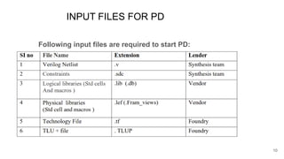
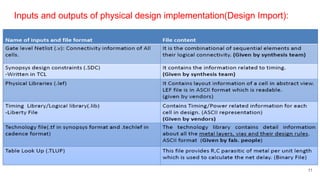
INPUT FILES FORPD
Following input files are required to start PD:
10
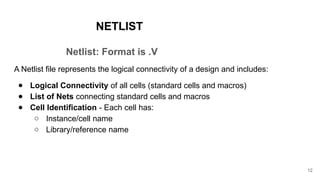
NETLIST
Netlist: Format is.V
A Netlist file represents the logical connectivity of a design and includes:
● Logical Connectivity of all cells (standard cells and macros)
● List of Nets connecting standard cells and macros
● Cell Identification - Each cell has:
○ Instance/cell name
○ Library/reference name
12
13.
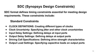
SDC (Synopsys DesignConstraints)
SDC format defines timing constraints essential for meeting design
requirements. These constraints include:
Standard Constraints
● CLOCK DEFINITIONS: Creating different types of clocks
● Clock Uncertainty: Specifying jitter and other clock uncertainties
● Input Delay Settings: Defining delays at input ports
● Output Delay Settings: Defining delays at output ports
● Driving Cell Specifications: Defining drive strength characteristics
● Output Load Settings: Specifying capacitive loads on output ports
13
14.
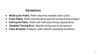
Exceptions
● Multi-cycle Paths:Paths requiring multiple clock cycles
● False Paths: Paths that should be ignored during timing analysis
● Half-cycle Paths: Paths with half-cycle timing requirements
● Disabled Timing Arcs: Specific timing arcs to be ignored
● Case Analysis: Analysis under specific operating conditions
14
15.
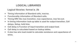
LOGICAL LIBRARIES
Logical libraries:format is .lib
● Timing information of Standard cells, macros.
● Functionality information of Standard cells.
● Timing DRV like max transition, max capacitance, max fan-out.
● In timing information look-up table is used for output transition, Cell
delays, Setup, hold time.
● Cell delay is Function of input transition and output load.
● Cell delay is calculated based on lookup tables.
● It also has wire load model to calculate resistance and capacitance of
wires.
15
16.
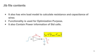
● It alsohas wire load model to calculate resistance and capacitance of
wires
● Functionality is used for Optimization Purpose.
● It also Contain Power information of Std cells.
16
.lib file contents
17.
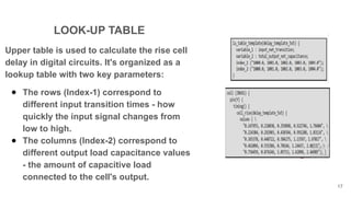
LOOK-UP TABLE
17
Upper tableis used to calculate the rise cell
delay in digital circuits. It's organized as a
lookup table with two key parameters:
● The rows (Index-1) correspond to
different input transition times - how
quickly the input signal changes from
low to high.
● The columns (Index-2) correspond to
different output load capacitance values
- the amount of capacitive load
connected to the cell's output.
18.
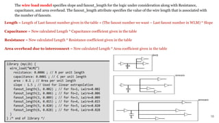
The wire loadmodel specifies slope and fanout_length for the logic under consideration along with Resistance,
capacitance, and area overhead. The fanout_length attribute specifies the value of the wire length that is associated with
the number of fanouts.
18
Length = Length of Last fanout number given in the table + (The fanout number we want – Last fanout number in WLM) * Slope
Capacitance = New calculated Length * Capacitance coefficient given in the table
Resistance = New calculated Length * Resistance coefficient given in the table
Area overhead due to interconnect = New calculated Length * Area coefficient given in the table
19.
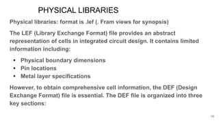
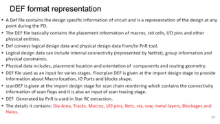
PHYSICAL LIBRARIES
Physical libraries:format is .lef (. Fram views for synopsis)
The LEF (Library Exchange Format) file provides an abstract
representation of cells in integrated circuit design. It contains limited
information including:
● Physical boundary dimensions
● Pin locations
● Metal layer specifications
However, to obtain comprehensive cell information, the DEF (Design
Exchange Format) file is essential. The DEF file is organized into three
key sections:
19
20.
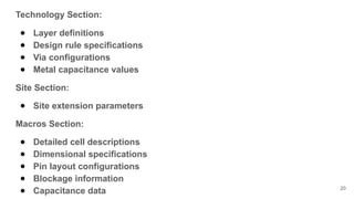
Technology Section:
● Layerdefinitions
● Design rule specifications
● Via configurations
● Metal capacitance values
Site Section:
● Site extension parameters
Macros Section:
● Detailed cell descriptions
● Dimensional specifications
● Pin layout configurations
● Blockage information
● Capacitance data 20
21.
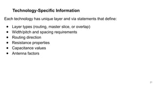
Technology-Specific Information
Each technologyhas unique layer and via statements that define:
● Layer types (routing, master slice, or overlap)
● Width/pitch and spacing requirements
● Routing direction
● Resistance properties
● Capacitance values
● Antenna factors
21
22.
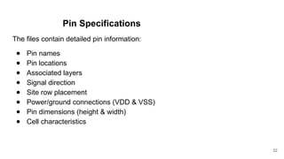
Pin Specifications
The filescontain detailed pin information:
● Pin names
● Pin locations
● Associated layers
● Signal direction
● Site row placement
● Power/ground connections (VDD & VSS)
● Pin dimensions (height & width)
● Cell characteristics
22
23.
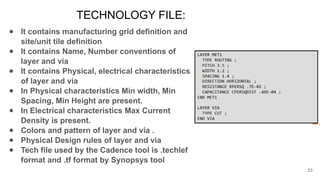
TECHNOLOGY FILE:
● Itcontains manufacturing grid definition and
site/unit tile definition
● It contains Name, Number conventions of
layer and via
● It contains Physical, electrical characteristics
of layer and via
● In Physical characteristics Min width, Min
Spacing, Min Height are present.
● In Electrical characteristics Max Current
Density is present.
● Colors and pattern of layer and via .
● Physical Design rules of layer and via
● Tech file used by the Cadence tool is .techlef
format and .tf format by Synopsys tool
23
24.
TLU PLUS
TLU+ (TableLook-Up Plus) is a binary table format specifically designed to
store RC (Resistance-Capacitance) Coefficients. These files provide several
key advantages:
● They enable accurate RC extraction by accounting for multiple factors
affecting resistance coefficients:
○ Width variations
○ Spacing considerations
○ Density effects
○ Temperature changes
24
25.
Mapping Function
The associatedmap file serves as a translation layer between different naming
conventions:
● It correlates layer and via names in the Milkyway technology file with
corresponding names in the ITF (Interconnect Technology Format) file
Primary Functions
● TLU+ files perform critical tasks in the design process:
● Determining the resistance and capacitance parasitics of metal per unit length
● Providing essential data for calculating net delays
● Serving as the primary source for parasitic data (when TLU+ files are
unavailable, this information is extracted from the .ITF file instead)
25
26.
Implementation Requirements
● Toproperly implement TLU+ files in a design flow:
● Three distinct files must be loaded:
○ Maximum TLU+ file
○ Minimum TLU+ file
○ Map file
● The map file establishes the connection between the .ITF file and the .tf file
for layer and via naming conventions
26
27.
MAP file.
● MAPfile maps the layer and via names of TLU+ file and .tf file .MAP
file maps the layer and via names of TLU+ file and .tf file.
UPF- File (Unified Power Format)
● UPF is designed to reflect the power intent of a design at a relatively
high level.
● UPF scripts describe which power rails should be routed to individual
blocks, when blocks are expected to be powered up or shut
down(primary power supply to a domain is removed)
● It describes how voltage levels should be shifted as signals cross from
one power domain to another and whether measures should be taken to
retain register and memory-cell contents if the primary power supply to
a domain is removed
27
28.
Floor Planning
The floorplanis a crucial foundation of physical design that significantly
impacts the quality of your chip implementation. A well-executed
floorplan streamlines the entire implementation process (placement,
clock tree synthesis, routing, and timing closure), while a poor floorplan
creates cascading issues throughout the design.
Impact of Floorplan Quality
Benefits of an excellent floorplan:
● Simplifies implementation process
● Reduces congestion
28
29.
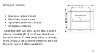
● Improves timingclosure
● Minimizes noise issues
● Optimizes power distribution
● Enhances reliability
A bad floorplan will blow up the area, power &
affects reliability,life of the IC and also it can
increase overall IC cost (more effort to closure,
more LVTs/ULVTs). A bad floorplan will blow up
the area, power & affects reliability,
29
Optimized Floorplan
30.
● Improves timingclosure
● Minimizes noise issues
● Optimizes power distribution
● Enhances reliability
30
31.
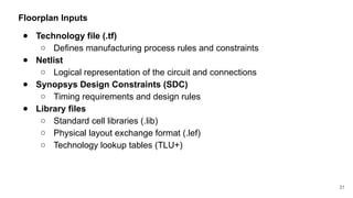
Floorplan Inputs
● Technologyfile (.tf)
○ Defines manufacturing process rules and constraints
● Netlist
○ Logical representation of the circuit and connections
● Synopsys Design Constraints (SDC)
○ Timing requirements and design rules
● Library files
○ Standard cell libraries (.lib)
○ Physical layout exchange format (.lef)
○ Technology lookup tables (TLU+)
31
32.
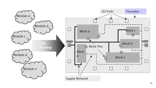
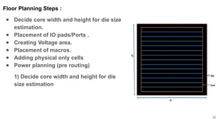
Floor Planning Steps:
● Decide core width and height for die size
estimation.
● Placement of IO pads/Ports .
● Creating Voltage area.
● Placement of macros.
● Adding physical only cells
● Power planning (pre routing)
1) Decide core width and height for die
size estimation
32
33.
Core area dependsupon:
Aspect ratio: Aspect ratio will decide the size and shape of the chip. ratio of height
and width of core.
Aspect ratio = width/height
Core utilization: - Utilization will define the area occupied by the standard cells,
macros, and other cells. If core utilization is 0.8 (80%) that means 80% of the core
area is used for placing the standard cells, macros, and other cells, and the
remaining
20% is used for routing purposes.
core utilization = (macros area + std cell area )/ total core area 33
34.
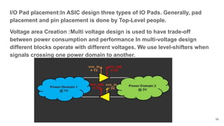
I/O Pad placement:InASIC design three types of IO Pads. Generally, pad
placement and pin placement is done by Top-Level people.
Voltage area Creation :Multi voltage design is used to have trade-off
between power consumption and performance In multi-voltage design
different blocks operate with different voltages. We use level-shifters when
signals crossing one power domain to another.
34
35.
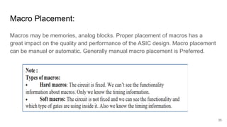
Macro Placement:
Macros maybe memories, analog blocks. Proper placement of macros has a
great impact on the quality and performance of the ASIC design. Macro placement
can be manual or automatic. Generally manual macro placement is Preferred.
35
36.
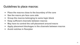
Guidelines to placemacros:
● Place the macros close to the boundary of the core
● See the macro pin face core side
● Group the macros belonging to same logic block
● Keep sufficient channels between macros
● May have to control the cell placement around macro
● Apply placement blockages in the channels between macros
● Avoid notches in floorplan
36
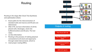
Routing
Routing is thestage after Clock Tree Synthesis
and optimization where:
● Exact paths for the interconnection of
standard cells and macros and I/O pins are
determined.
● After CTS, we have information of all the
placed cells, blockages, clock tree
buffers/inverters and I/O pins. The tool
relies
● on this information.
● Routing is the process of making physical
connections to all clock and signal pins
through metal interconnects, which to
● meet proper routing DRCs.
39
40.
Routing Objective:
● Thereshould be no Timing (drv’s , setup and hold) and DRC violation.
● Establishing connectivity with minimum no. of vias
Routing Prerequisites:
● CTS and optimization should be complete.
● The measured congestion should be acceptable.
● Timing DRC violations and Timing QoR estimated after CTS must be
acceptable.
● The PG nets must be pre-routed and physically connected to all macros
and standard cells.
40
41.
Inputs of routing:
●CTS DEF file
● CTS Netlist (.v)
● Synopsys design constraints (SDC)
● Timing library/logical library(.Lib), Physical library(.Lef)
● Technology file (.tf)
● TLU+(Table Look Up)
Goals of Routing:
● Minimize the total interconnect/wire length and congestion hotspots.
● Complete the connections without increasing the total area of the block.
● Minimize the number of layer changes that the connections have to
make (minimizing the number vias).
41
42.
The different tasksthat are performed in the routing stage are as follows:
● Global Routing.
● Track assignment.
● Detailed Routing.
● Search and Repair.
Global Routing:
● GR first partitions the routing region into tiles/rectangles called global
routing cells (g-cells) and decides tile-to-tile paths for all nets while
attempting to optimize some given objective function (e.g. total wire
length and circuit timing), But doesn’t make actual connections or
assign nets to specific paths within the routing regions.
42
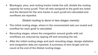
43.
● Blockages, pins,and routing tracks inside the cell, dictate the routing
capacity for every g-cell. Then all nets assigned to the gcell are noted
and the demand for the wire tracks in each g-cell are calculated and
overflows are reported.
Global routing is done in two stages namely:
● The initial routing stage, where in the unconnected nets are routed and
overflow for each gcell is calculated.
● Rerouting stages, where the congestion around gcells with net
overflows are reduced by ripping off and rerouting the net.
● After the initial routing stage and each rerouting stage, design statistics
and congestion data are reported. A summary of wire length and via
count at the end of the Global routing stage.
43
44.
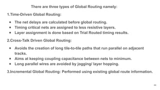
There are threetypes of Global Routing namely:
1.Time-Driven Global Routing:
● The net delays are calculated before global routing.
● Timing critical nets are assigned to less resistive layers.
● Layer assignment is done based on Trial Routed timing results.
2.Cross-Talk Driven Global Routing:
● Avoids the creation of long tile-to-tile paths that run parallel on adjacent
tracks.
● Aims at keeping coupling capacitance between nets to minimum.
● Long parallel wires are avoided by jogging/ layer hopping.
3.Incremental Global Routing: Performed using existing global route information.
44
45.
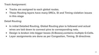
Track Assignment:
● Tracksare assigned to each global routes.
● These Routing layers have many DRCs, SI and Timing violation issues
in this stage
Detail Routing:
● In initial Detailed Routing, Global Routing plan is followed and actual
wires are laid down to connect pins to corresponding nets.
● Design is broken into bigger boxes (S-Boxes),contains multiple G-Cells.
● Layer assignments are done as per Congestion, Timing, SI directives
45
46.
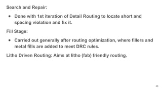
Search and Repair:
●Done with 1st iteration of Detail Routing to locate short and
spacing violation and fix it.
Fill Stage:
● Carried out generally after routing optimization, where fillers and
metal fills are added to meet DRC rules.
Litho Driven Routing: Aims at litho (fab) friendly routing.
46
47.
Checklist After Routing
●Timing (drv’s , setup and hold)
● Drc’s ( design rule checks )
● Core utilization, Cell legality, Congestion
● Power Analysis must be done and total Power
Consumption in Design.
47
48.
ROUTING OPTIMIZATION
● Routingoptimization is a step performed after detailed routing
in the flow.
● Inaccurate modeling of the routing topology may cause timing,
signal integrity(noise, cross-talk) and logical design constraint
related
● violations.
● This may cause conditions where in fixing a violation would
create other violations and many such scenarios may cascade to
make it very
● difficult for timing closure with no timing DRCs.
● Hence it is necessary to fix and optimize the routing topology.
48
49.
Routing optimization involves
●Fixing timing violations.
● Fixing LVS (opens & shorts).
● Fixing DRCs.
● Fixing Timing DRCs (Meet max transition, max capacitance and max
fanout).
● Finding & Fixing Antenna violations (using jumpers and antenna
diodes).
● Area and Leakage power recovery.
● Fixing SI related issues.
● Redundant via insertion.
49
50.
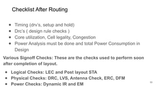
Checklist After Routing
●Timing (drv’s, setup and hold)
● Drc’s ( design rule checks )
● Core utilization, Cell legality, Congestion
● Power Analysis must be done and total Power Consumption in
Design
50
Various Signoff Checks: These are the checks used to perform soon
after completion of layout.
● Logical Checks: LEC and Post layout STA
● Physical Checks: DRC, LVS, Antenna Check, ERC, DFM
● Power Checks: Dynamic IR and EM