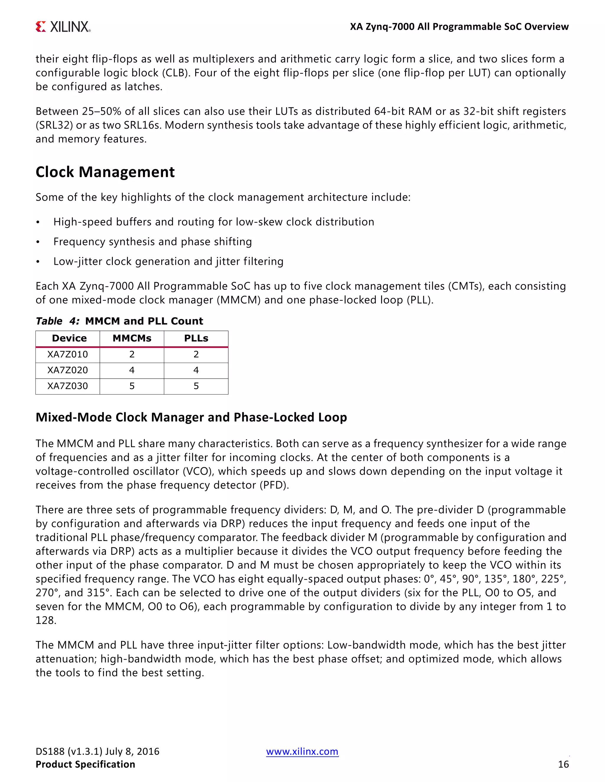
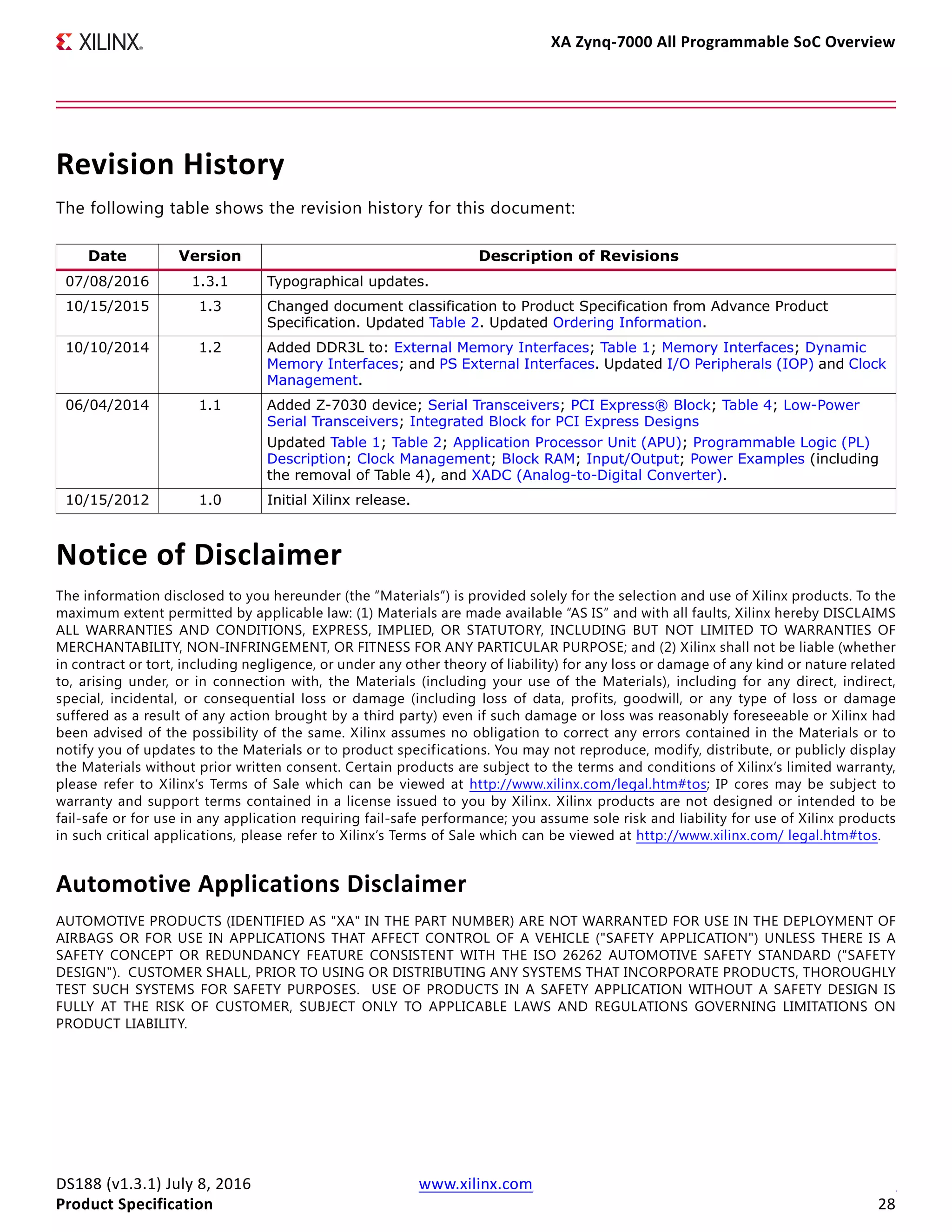
Download to read offline
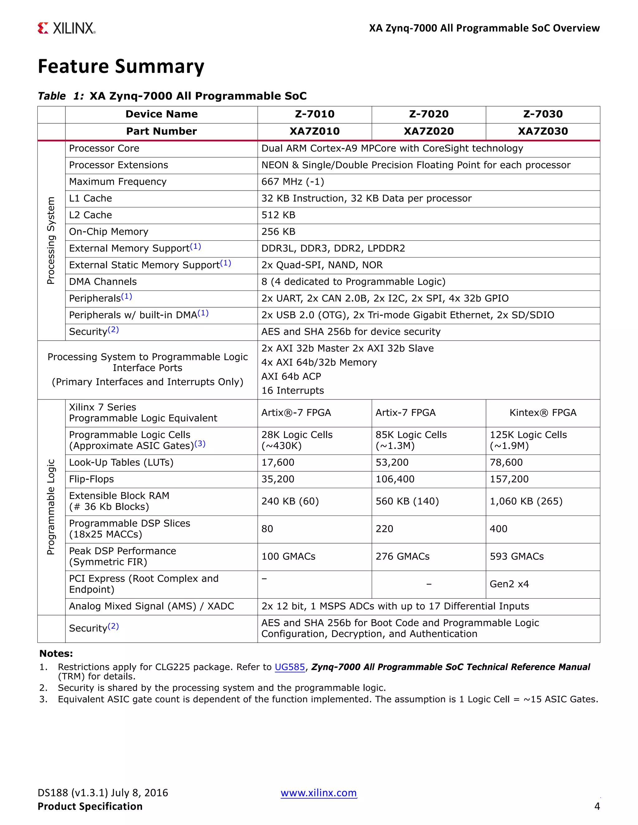
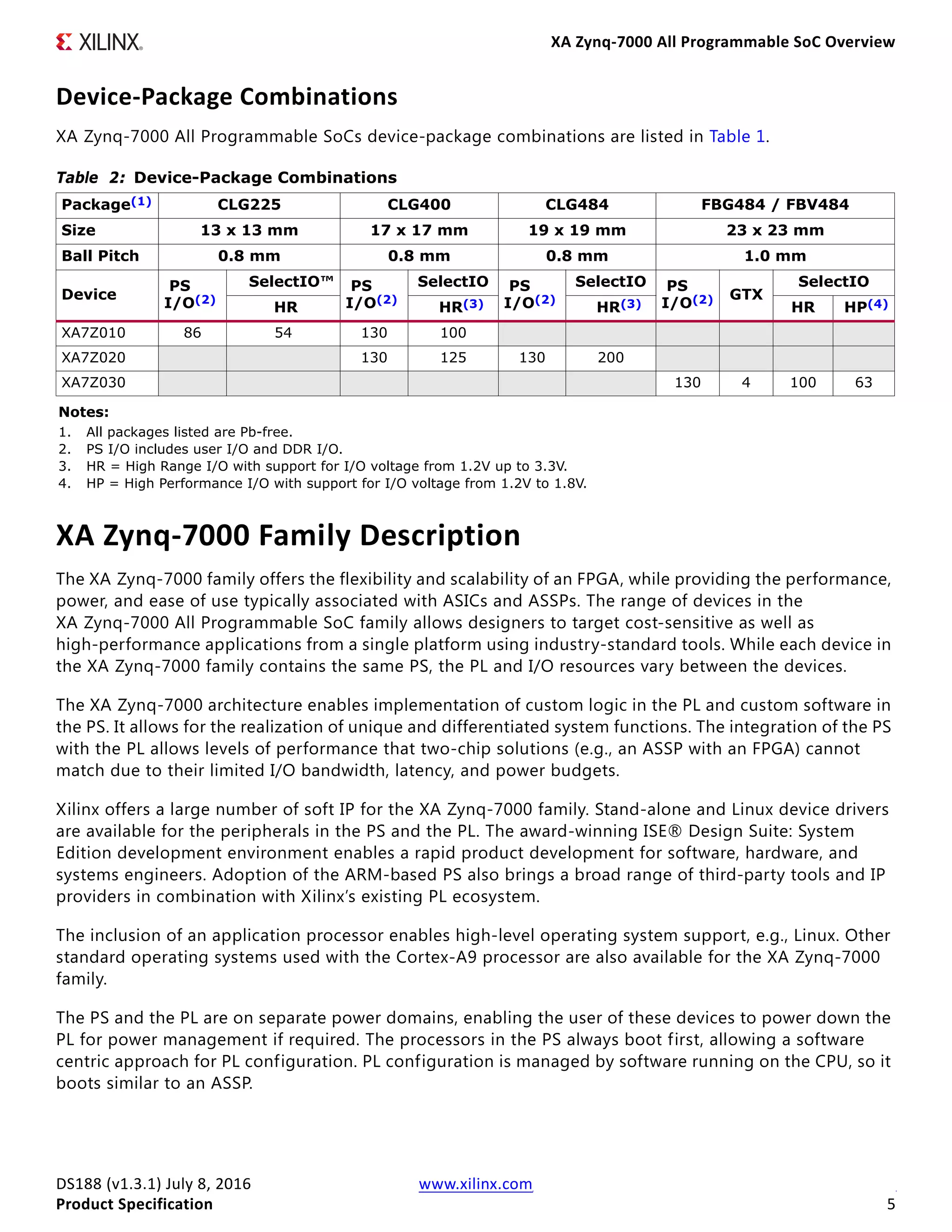
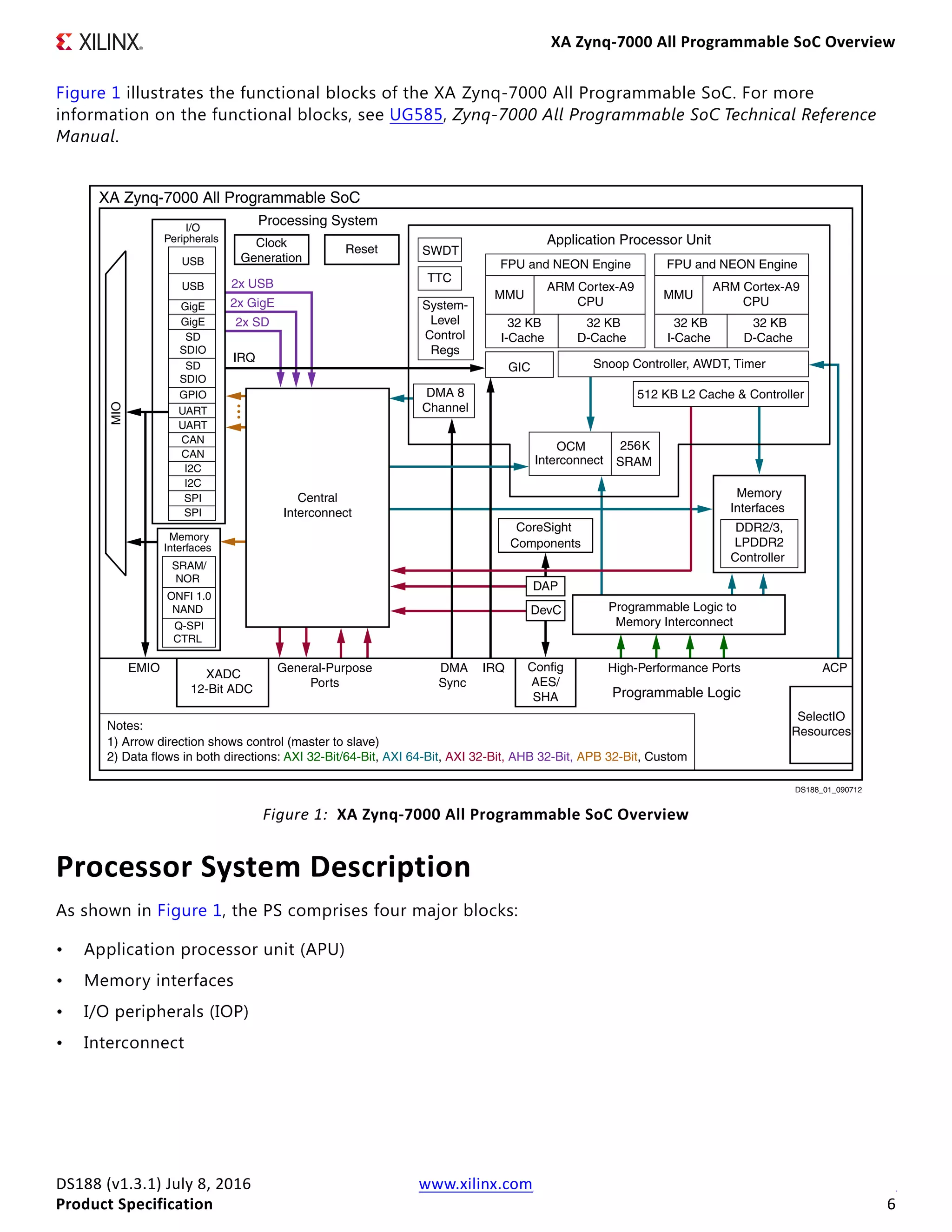

The document describes the XA Zynq-7000 All Programmable SoC, which integrates a dual-core ARM Cortex-A9 processor and programmable logic. The processor system includes the application processor unit with two 667MHz Cortex-A9 cores, on-chip memory, external memory interfaces, and peripherals. It connects to the programmable logic through high-bandwidth interfaces. The programmable logic contains logic resources like LUTs and block RAM, as well as DSP slices. The SoC provides processing system and programmable logic integration in a single device for applications requiring both processing and custom logic.