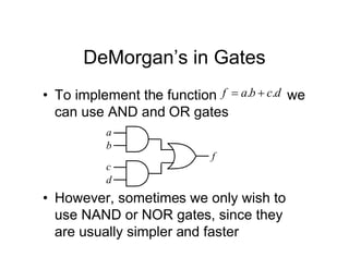
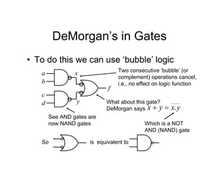
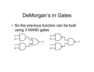
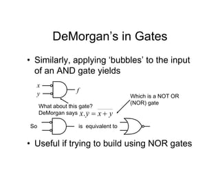
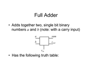
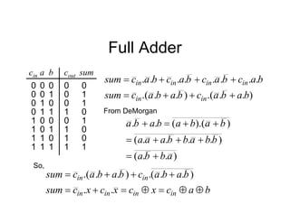
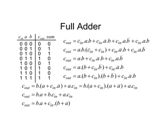
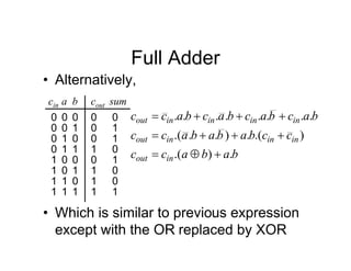
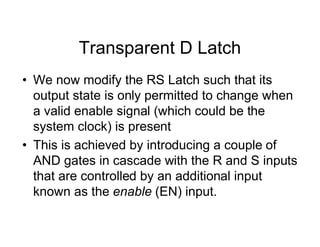
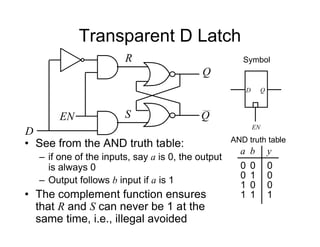
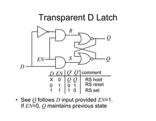
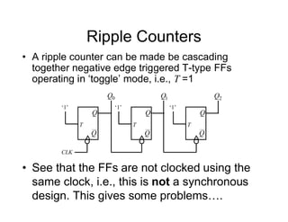
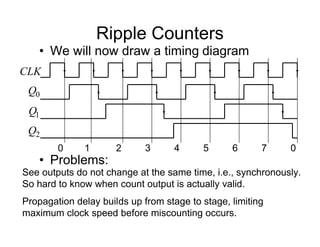
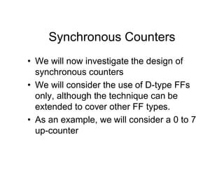
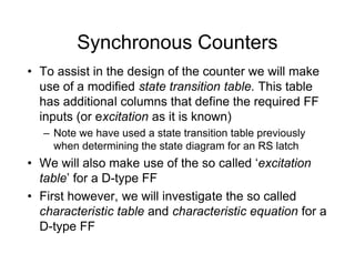
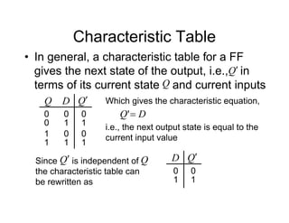
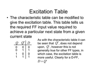
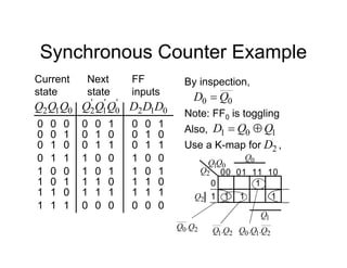
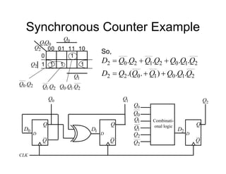
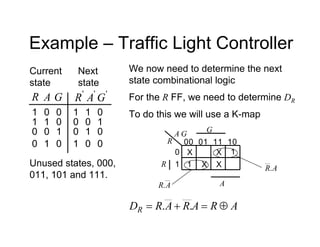
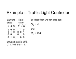
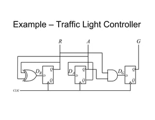
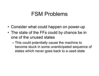
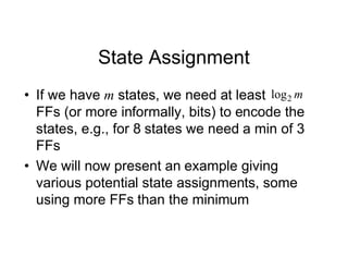
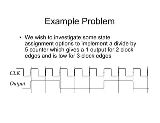
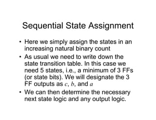
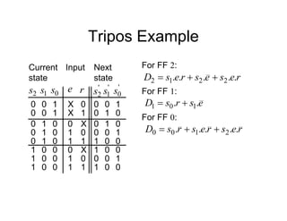
This document provides an overview of a course on digital electronics that covers combinational and sequential logic. The course consists of 11 lectures and 6 hardware lab workshops. The objectives are for students to learn about combinational and sequential logic circuits, how digital logic gates are built using transistors, and how to design and construct simple digital electronic systems. Key topics that will be covered include Boolean algebra, logic gates, combinational logic, sequential logic, and how digital systems are constructed from semiconductors to computers. Recommended textbooks are also listed.


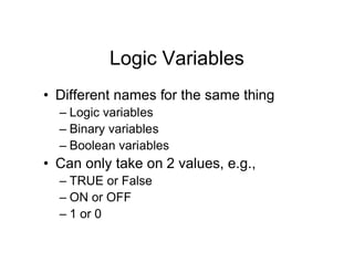

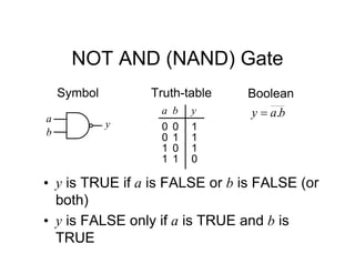

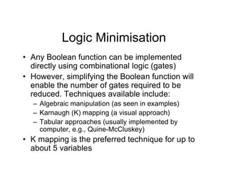
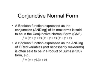

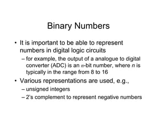
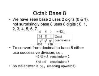
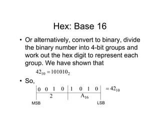
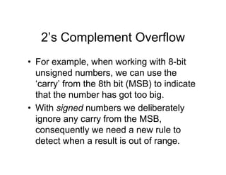
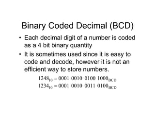


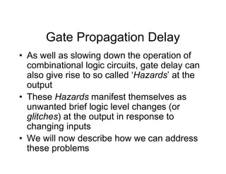


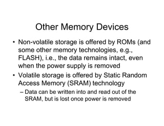
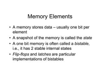
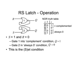
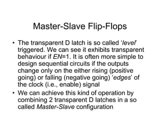

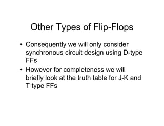
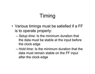
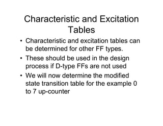
![Tripos Example
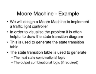
• The state diagram for a synchroniser is shown.
It has 3 states and 2 inputs, namely e and r.
The states are mapped using sequential
assignment as shown.
[s1 s0]
FF labels
Sync Hunt
Sight
[10] [00]
[01]
r
r
r
e.
r
e.
r
e. r
e.
e
e
An output, s should be
true if in Sync state](https://image.slidesharecdn.com/debasicspdf-240215175513-2e86b8f3/85/Digital-Electronics-basics-book1_pdf-pdf-212-320.jpg)
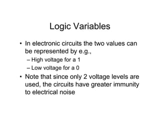
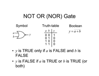
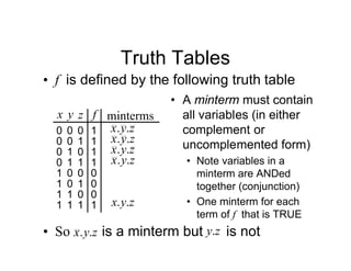
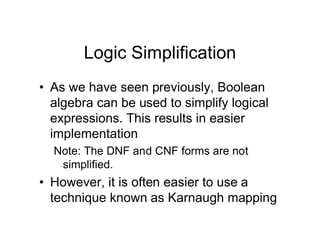
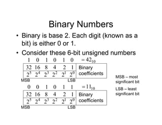
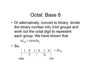
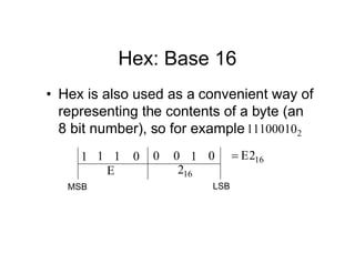
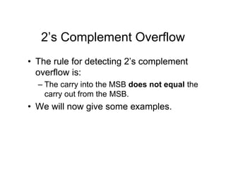
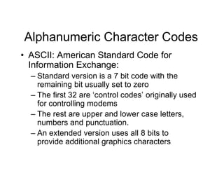
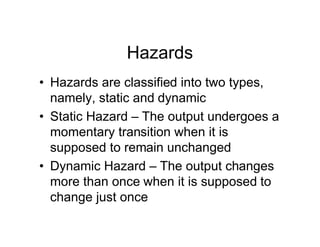
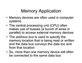
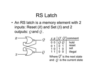
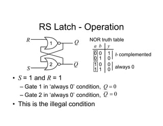
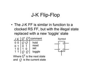
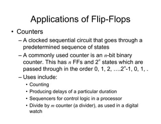
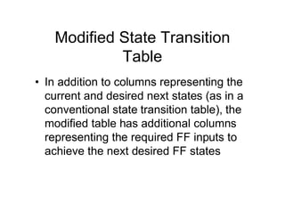
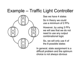
![Tripos Example
Sync Hunt
Sight
[10] [00]
[01]
r
r
r
e.
r
e.
r
e. r
e.
e
e
Unused state 11
Current
state
r
e
0
X
1
X
'
1
s '
0
s
0
1
0
0
Next
state
0
s
0
0
0
0
Input
1
s
X
0 1
0
0
1 0
0
1
0
1
0
1
1 0
1
1
0
0
1 0
0
0
1
X
0 0
1
0
1
1
1 0
1
0
1
X
X X
X
1
1
From inspection, 1
s
s ](https://image.slidesharecdn.com/debasicspdf-240215175513-2e86b8f3/85/Digital-Electronics-basics-book1_pdf-pdf-213-320.jpg)
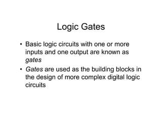
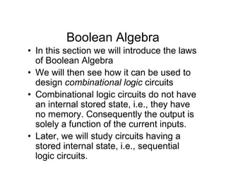
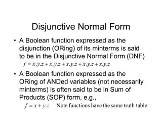
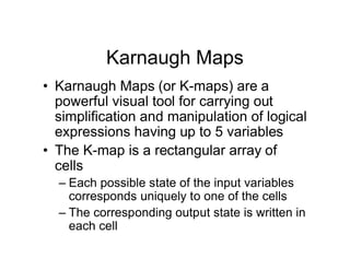
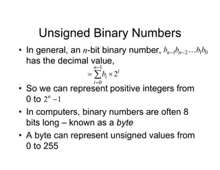
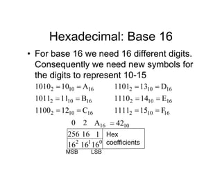
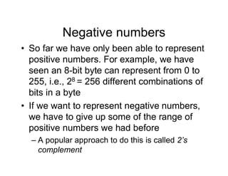
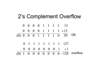
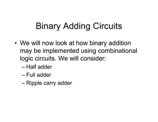
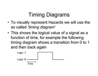
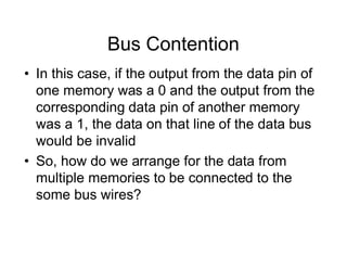
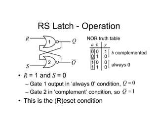
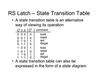
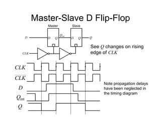
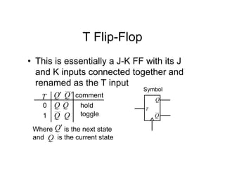
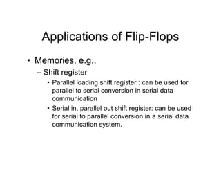
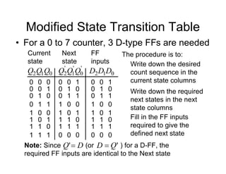
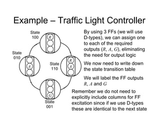
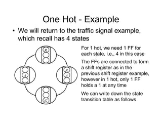
![Tripos Example
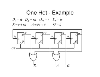
• We will now re-implement the synchroniser
using a 1 hot approach
• In this case we will need 3 FFs
Sync Hunt
Sight
[100] [001]
[010]
r
r
r
e.
r
e.
r
e. r
e.
e
e
[s2 s1 s0]
FF labels
An output, s should be
true if in Sync state
From inspection, 2
s
s ](https://image.slidesharecdn.com/debasicspdf-240215175513-2e86b8f3/85/Digital-Electronics-basics-book1_pdf-pdf-216-320.jpg)
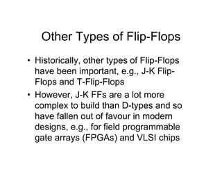
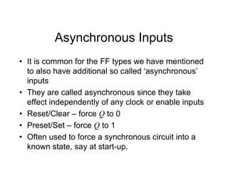
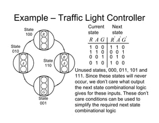
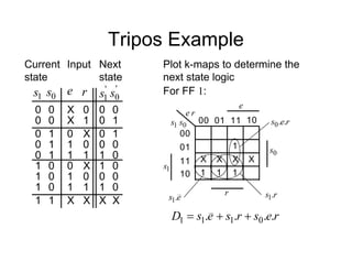
![Tripos Example
Sync Hunt
Sight
[100] [001]
[010]
r
r
r
e.
r
e.
r
e. r
e.
e
e
Current
state
r
e
0
X
1
X
'
2
s
0
0
Next
state
0
s
1
1
Input
X
0 0
0
1 0
0
0
1
1 1
0
0
1 0
0
X
0 1
0
1
1 1
0
'
1
s
0
1
1
0
0
0
0
0
0
0
1
s
1
1
1
0
0
0
'
0
s
1
0
0
1
0
1
0
0
0
0
2
s
0
0
0
1
1
1
Remember when interpreting this table, because of the 1-
hot shift structure, only 1 FF is 1 at a time, consequently it
is straightforward to write down the next state equations](https://image.slidesharecdn.com/debasicspdf-240215175513-2e86b8f3/85/Digital-Electronics-basics-book1_pdf-pdf-217-320.jpg)
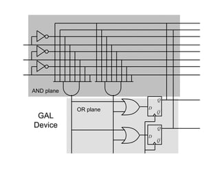
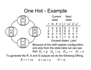
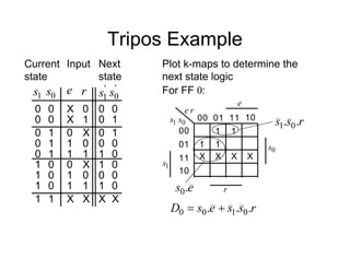
![Tripos Example
Sync Hunt
Sight
[100] [001]
[010]
r
r
r
e.
r
e.
r
e. r
e.
e
e
Note that it is not strictly
necessary to write down the
state table, since the next state
equations can be obtained from
the state diagram
It can be seen that for each
state variable, the required
equation is given by terms
representing the incoming arcs
on the graph
For example, for FF 2: r
e
s
e
s
r
e
s
D .
.
.
.
. 2
2
1
2
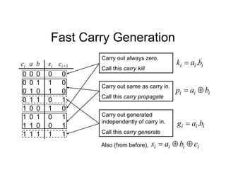
Also note some simplification is possible by noting that:
1
0
1
2
s
s
s (which is equivalent to e.g., )
0
1
2 s
s
s
](https://image.slidesharecdn.com/debasicspdf-240215175513-2e86b8f3/85/Digital-Electronics-basics-book1_pdf-pdf-219-320.jpg)