What are the advantages and disadvantages of membrane structures.pptx
DE Unit1-3-13 (1).pdf
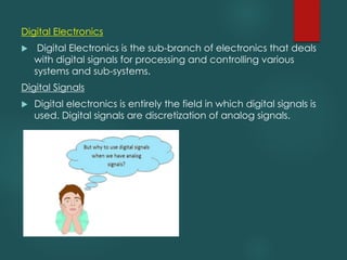
1. Digital Electronics
u Digital Electronics is the sub-branch of electronics that deals
with digital signals for processing and controlling various
systems and sub-systems.
Digital Signals
u Digital electronics is entirely the field in which digital signals is
used. Digital signals are discretization of analog signals.
2. u Analog signals are more likely to get affected by noise,
while digital signals are noise immune. Besides, the
designing and operations of a digital circuit is simpler than
analog circuit.
u It is better to use digital signals if we need accurate and
precised operation of the devices.
3.
4. Advantages of Digital Systems
u Easier Designing: The Digital systems can be easily designed as they involve
digital signals. It comprises of basically two values 0 and 1 .
u Noise Immune: The analog signal will be affected more because it varies
continuous with time so it is difficult to identify that noise has destroyed
which value of voltage. While in case of digital system, noise effect the
particular range of the signal thus, it is clear to identify the particular range
of filtering is also easy in case of digital signals.
u Information Storage is Simpler: The storage of information in digital systems is
easy.
u High Accuracy And Precision: The digital signal offers high accuracy and
precision. This is because the processing of digital signal is done through the
switching circuit.
u Programmable: The digital systems are easily programmable but analog
system becomes complex when excessive programming of components is
done.
Disadvantages of Digital Systems
u Expensive: Digital systems are expensive because it involves switching
elements.
u Analog nature of Real World Entities: We need to convert the digital output
in analog form because all the real world entities are analog.
5. Why is it named Digital ?
u Digital systems deal with things that are in one of two distinct
states. The easiest example is anything that is either on or off. If
you look at many devices today, you will find that the on/off
switch is a single push button with the symbol shown in Figure .
u This icon represents a 1 and a 0, the numerical digits used to
describe the two states in a digital system. We use numeric
digits 0 and 1 to represent the two states off and on,
respectively. Since there are only two digits, we call them
binary digits, or bits .
6. Digital Hardware
u Logic circuits are used to build computer hardware, as well as
many other types of products. All such products are broadly
classified as digital hardware.
u A computer is a common digital system. Hardware refers to the
physical parts of the computer that you can touch. A desktop
computer includes the case (or tower), the monitor, keyboard and
mouse.
u The technology used to build digital hardware has evolved
dramatically over the past four decades. Until the 1960s logic
circuits were constructed with bulky components, such as
transistors and resistors that came as individual parts. The advent of
integrated circuits made it possible to place a number of
transistors, and thus an entire circuit, on a single chip.
u For most digital hardware products, it is also necessary to design
and build some logic circuits from scratch. For implementing these
circuits, three main types of chips may be used: standard chips,
programmable logic devices, and custom chips.
8. Design of Digital Hardware
u Assuming that we have a design concept for a large circuit.
u An orderly way of dealing with the complexity involved is to
partition the circuit into smaller blocks and then to design each
block separately.
u The interconnection between the blocks must be defined,
which effectively combines these blocks into a single large
circuit.
u Now it is necessary to simulate this complete circuit and correct
any errors. Depending on the errors encountered, it may be
necessary to go back to the previous steps as indicated by the
paths A, B, and C in the flowchart.
u Successful completion of functional simulation suggests that the
designed circuit will correctly perform all of its functions. The
next step is to decide how to realize this circuit on a PCB. The
physical location of each chip on the board has to be
determined, and the wiring pattern needed to make
connections between the chips has to be defined. This step is
known as physical design of the PCB.
9. u Some errors may be caused by incorrect connections between
the blocks, in which case these connections have to be
redefined, following path C.
u Some blocks may not have been designed correctly, in which
case path B is followed and the erroneous blocks are redesigned.
u Another possibility is that the very first step of partitioning the
overall large circuit into blocks was not done well, in which case
path A is followed.
u A timing simulation may reveal potential performance problems,
which can then be corrected by using the CAD tools to make
changes in the physical design of the PCB. Having completed the
design process, the designed circuit is ready for physical
implementation.
10.
11. u The PCB in the figure contains one processor chip and various
memory and support chips. Complex logic circuits are needed to
form the interface between the processor and the rest of the
system.