Download to read offline
![1999 Sep 28 3
Philips Semiconductors Preliminary Device Specification
TV signal processor-Teletext decoder with
embedded µ-Controller
TDA935X/6X/8X series
µ-Controller
• 80C51 µ-controller core standard instruction set and
timing
• 1 µs machine cycle
• 32 - 128Kx8-bit late programmed ROM
• 3 - 12Kx8-bit Auxiliary RAM (shared with Display and
Acquisition)
• Interrupt controller for individual enable/disable with two
level priority
• Two 16-bit Timer/Counter registers
• WatchDog timer
• Auxiliary RAM page pointer
• 16-bit Data pointer
• IDLE and Power Down (PD) mode
• 14 bits PWM for Voltage Synthesis Tuning
• 8-bit A/D converter
• 4 pins which can be programmed as general I/O pin,
ADC input or PWM (6-bit) output
Data Capture
• Text memory for 1 or 10 pages
• In the 10 page versions inventory of transmitted Teletext
pages stored in the Transmitted Page Table (TPT) and
Subtitle Page Table (SPT)
• Data Capture for US Closed Caption
• Data Capture for 525/625 line WST, VPS (PDC system
A) and Wide Screen Signalling (WSS) bit decoding
• Automatic selection between 525 WST/625 WST
• Automatic selection between 625 WST/VPS on line 16
of VBI
• Real-time capture and decoding for WST Teletext in
Hardware, to enable optimized µ-processor throughput
• Automatic detection of FASTEXT transmission
• Real-time packet 26 engine in Hardware for processing
accented, G2 and G3 characters
• Signal quality detector for video and WST/VPS data
types
• Comprehensive teletext language coverage
• Full Field and Vertical Blanking Interval (VBI) data
capture of WST data
Display
• Teletext and Enhanced OSD modes
• Features of level 1.5 WST and US Close Caption
• Serial and Parallel Display Attributes
• Single/Double/Quadruple Width and Height for
characters
• Scrolling of display region
• Variable flash rate controlled by software
• Enhanced display features including overlining,
underlining and italics
• Soft colours using CLUT with 4096 colour palette
• Globally selectable scan lines per row (9/10/13/16) and
character matrix [12x10, 12x13, 12x16 (VxH)]
• Fringing (Shadow) selectable from N-S-E-W direction
• Fringe colour selectable
• Meshing of defined area
• Contrast reduction of defined area
• Cursor
• Special Graphics Characters with two planes, allowing
four colours per character
• 32 software redefinable On-Screen display characters
• 4 WST Character sets (G0/G2) in single device (e.g.
Latin, Cyrillic, Greek, Arabic)
• G1 Mosaic graphics, Limited G3 Line drawing
characters
• WST Character sets and Closed Caption Character set
in single device](https://image.slidesharecdn.com/datasheet-191115162427/85/Datasheet-3-320.jpg)


![Philips Semiconductors Preliminary specification
1999 Sep 28 12
TV signal processor-Teletext decoder with
embedded µ-Controller
TDA 935X/6X/8X series
Microcontroller
The functionality of the microcontroller used on the device is described here with reference to the industry
standard 80C51 microcontroller. A full description of its functionality can be found in the "80C51 Based 8-Bit
Microcontrollers - Philips Semiconductors (ref. IC20)" (Reference [1])
Memory Organisation
The device has the capability of a maximum of 128K PROGRAM ROM and 12K DATA RAM internally.
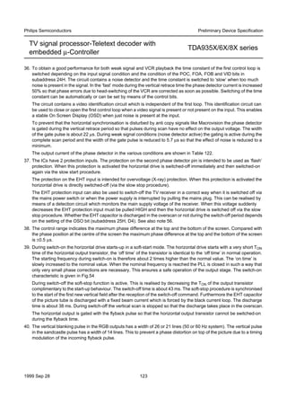
ROM BANK SWITCHING
Devices with up to 64K Program ROM have a continuous address space. Devices with over 64K Program ROM
use ROM bank switching. The 128K version is arranged in four banks of 32K. One of the 32K banks is common
and is always addressable. The other three banks(Bank0,Bank1,Bank2) can be accessed by selecting the right
bank via the SFR ROMBK bits 1/0.
Figure 5 ROM Bank Switching memory map
ROMBK<2:0> 0 to 32K 32K to 64K
00 Common Bank0
01 Common Bank1
10 Common Bank2
11 Reserved Reserved
Table 2 ROM Bank Selection
7FFFH
0000H
FFFFH
8000H 8000H 8000H
FFFFH FFFFH
Common
32K
Bank0
32K
Bank2
32K
Bank1
32K](https://image.slidesharecdn.com/datasheet-191115162427/85/Datasheet-12-320.jpg)


![Philips Semiconductors Preliminary specification
1999 Sep 28 33
TV signal processor-Teletext decoder with
embedded µ-Controller
TDA 935X/6X/8X series
PORT TYPE
All individual ports bits can be programmed to function in one of four modes, the mode is defined by eight Port
Configuration SFR’s (P0CFGA/P0CFGB, P1CFGA/P1CFGB, P2CFGA/P2CFGB and P3CFGA/P3CFGB). The
modes available are Open Drain, Quasi-bidirectional, High Impedance, Push-Pull.
Open Drain
The Open drain mode can be used for bi-directional operation of a port. It requires an external pull-up resistor,
the pull-up voltage has a maximum value of 5.5V, to allow connection of the device into a 5V environment.
Quasi-bidirectional
The quasi-bidirectional mode is a combination of open drain and push pull. It requires an external pull-up resistor
to VDDp (nominally 3.3V). When a signal transition from 0 to 1 is output from the device, the pad is put into push-
pull mode for one clock cycle (166ns) after which the pad goes into open drain mode. The mode may be used
to speed up the edges of signal transitions. This is the default mode of operation of the pads after reset.
High Impedance
The high impedance mode can be used for Input only operation of the port. When using this configuration the
two output transistors are turned off.
Push-Pull
The push pull mode can be used for output only. In this mode the signal is driven to either 0V or VDDp, which
is nominally 3.3V.
Interrupt System
The device has 7 interrupt sources, each of which can be enabled or disabled. When enabled each interrupt
can be assigned one of two priority levels. There are four interrupts that are common to the 80C51, two of these
are external interrupts (EX0 and EX1) and the other two are timer interrupts (ET0 and ET1). In addition to the
conventional 80c51, two application specific interrupts are incorporated internal to the device which have
following functionality:-
ECC (Closed Caption Data Ready Interrupt) - This interrupt is generated when the device is configured in
Closed Caption Acquisition mode. The interrupt is activated at the end of the currently selected Slice Line as
defined in the CCLIN SFR.
EBUSY (Display Busy Interrupt) - An interrupt is generated when the Display enters either a Horizontal or
Vertical Blanking Period. i.e. Indicates when the micro-controller can update the Display RAM without causing
undesired effects on the screen. This interrupt can be configured in one of two modes using the MMR
Configuration Register (Address 87FF, Bit-3 [TXT/V]):-
• TeXT Display Busy: An interrupt is generated on each active horizontal display line when the Horizontal
Blanking Period is entered.
• Vertical Display Busy: An interrupt is generated on each vertical display field when the Vertical Blanking
Period is entered.](https://image.slidesharecdn.com/datasheet-191115162427/85/Datasheet-33-320.jpg)


![Philips Semiconductors Preliminary specification
1999 Sep 28 36
TV signal processor-Teletext decoder with
embedded µ-Controller
TDA 935X/6X/8X series
TCON, TMOD, TL0, TH0, TL1 and TH1.
The Timer/Counter function is selected by control bits C/T in the Timer Mode SFR(TMOD). These two Timer/
Counter have four operating modes, which are selected by bit-pairs (M1.M0) in the TMOD. Details of the modes
of operation are given in the "80C51 Based 8-Bit Microcontrollers - Philips Semiconductors (ref. IC20)"
(Reference [1]).
TL0 and TH0 are the actual timer/counter registers for timer 0. TL0 is the low byte and TH0 is the high byte. TL1
and TH1 are the actual timer/counter registers for timer 1. TL1 is the low byte and TH1 is the high byte.
WatchDog Timer
The WatchDog timer is a counter that when it overflows forces the microcontroller in to a reset. The purpose of
the WatchDog timer is to reset the microcontroller if it enters an erroneous processor state (possibly caused by
electrical noise or RFI) within a reasonable period of time. When enabled, the WatchDog circuitry will generate
a system reset if the user program fails to reload the WatchDog timer within a specified length of time known as
the WatchDog interval.
The WatchDog timer consists of an 8-bit counter with an 11 bit prescaler. The prescaler is fed with a signal
whose frequency is 1/12 fosc (1MHz). The 8 bit timer is incremented every ‘t’ seconds where:
t=12x2048x1/fosc=12x2048x1/12x106
= 2.048ms
WATCHDOG TIMER OPERATION
The WatchDog operation is activated when the WLE bit in the Power Control SFR (PCON) is set. The WatchDog
can be disabled by Software by loading the value 55H into the WatchDog Key SFR (WDTKEY). This must be
performed before entering Idle/Power Down mode to prevent exiting the mode prematurely.
Once activated the WatchDog timer SFR (WDT) must be reloaded before the timer overflows. The WLE bit must
be set to enable loading of the WDT SFR, once loaded the WLE bit is reset by hardware, this is to prevent
erroneous Software from loading the WDT SFR.
The value loaded into the WDT defines the WatchDog interval.
WatchDog interval = (256 - WDT) * t = (256 -WDT)*2.048ms
The range of intervals is from WDT = 00H which gives 524ms to WDT = FFH which gives 2.048ms
PORT Alternate Functions
The Ports 1,2 and 3 are shared with alternate functions to enable control of external devices and circuitry. The
alternate functions are enabled by setting the appropriate SFR and also writing a logic ‘1’ to the Port bit that the
function occupies.
If the Pulse Width Modulator outputs (PWM) are required on Ports 3.0 to 3.3, they require an additional bit to be
set in the Character ROM. If this facility is required, it should be requested when ordering the Language Set.
The PWMs may be enabled per pin, thus giving any combination of either PWM output, SFR output or SAD
input.](https://image.slidesharecdn.com/datasheet-191115162427/85/Datasheet-36-320.jpg)


![Philips Semiconductors Preliminary specification
1999 Sep 28 39
TV signal processor-Teletext decoder with
embedded µ-Controller
TDA 935X/6X/8X series
SAD DC Comparator mode
The SAD module incorporates a DC Comparator mode which is selected using the ‘DC_COMP’ control bit in
the SADB SFR. This mode enables the microcontroller to detect a threshold crossing at the input to the selected
analog input pin (P3.0/ADC0, P3.1/ADC1, P3.2/ADC2 or P3.3/ADC3) of the software ADC. A level sensitive
interrupt is generated when the analog input voltage level at the pin falls below the analog output level of the
SAD Digital-to-Analog Converter.
This mode is intended to provide the device with a wake-up mechanism from Power-down or Idle mode when
a key-press on the front panel of the TV is detected.
The following software sequence should be used when utilizing this mode for Power-down or Idle mode:
1. Disable INT1 using the IE SFR
2. Set INT1 to level sensitive using the TCON SFR
3. Set the DAC digital input level to the desired threshold level using SAD/SADB SFRs and select the required
input pin (P3.0, P3.1, P3.2 or P3,3) using CH1 and CH0 in the SAD SFR
4. Enter DC Compare mode by setting the ‘DC_COMP’ enable bit in the SADB SFR
5. Enable INT1 using the IE SFR
6. Enter Power-down/Idle mode. Upon wake-up the SAD should be restored to its conventional operating mode
by disabling the ‘DC_COMP’ control bit.
I2C Serial I/O Bus
The I2
C bus consists of a serial data line (SDA on Port P1.7) and a serial clock line (SCL on Port P1.6).
These Ports may be enabled/disabled using TXT21.0 (I2
C Port Enable Bit).
Within the device, two separate hardware modules utilise this Bus: The Micro-controller and the TV Signal
Processor. The Micro-controller I2
C peripheral may operate in four different configurations:
• Master Transmitter
• Master Receiver
• Slave Transmitter
• Slave Receiver
The TV Signal Processor may be addressed in Slave Mode only, either via the 80C51 micro-controller or from
Port P1.6 and Port P1.7 by another master in the system.
I2C-bus control of the TV signal processor
For compatibility and possible re-use of software blocks, the I2
C-bus control for the TV signal processor is
organised as in the stand-alone TV signal processors. The internal communication is independent of the
programming of the Ports P1.6 and P1.7. All details on the control of the TV signal processor are given in the
description of the TV signal processor.
The byte level I2
C serial port on the device is identical in operation/configuration to the I2
C serial port on the
8xC558, with the exception of the clock rate selection bits CR<2:0>. The operation of the I2
C subsystem is
described in detail in the 8xC558 datasheet contained in reference [1].](https://image.slidesharecdn.com/datasheet-191115162427/85/Datasheet-39-320.jpg)


![Philips Semiconductors Preliminary specification
1999 Sep 28 46
TV signal processor-Teletext decoder with
embedded µ-Controller
TDA 935X/6X/8X series
Multi Rate Video Input Processor
The multi rate video input processor is a Digital Signal Processor designed to extract the data in serial form and
recover the clock from a digitised CVBS signal.
DATA STANDARDS
The data and clock standards that can be recovered are shown in Table 12.
Data Capture Timing
The Data Capture timing section uses the Synchronisation information extracted from the CVBS signal to
generate the required Horizontal and Vertical reference timings.
The timing section automatically recognises and selects the appropriate timings for either 625 (50Hz)
synchronisation or 525 (60Hz) synchronisation. A flag TXT12.Video Signal Quality is set when the timing section
is locked correctly to the incoming CVBS signal. When TXT12.Video Signal Quality is set another flag
TXT12.625/525 SYNC can be used to identify the standard.
Acquisition
The acquisition sections extracts the relevant information from the serial data stream received from the MulVIP
section and writes it in to display memory.
WST ACQUISITION
The device is capable of acquiring level 1.5 625 Line and 525 Line World System Teletext (see Reference [3]
and Reference [4]]).
BROADCAST SERVICE DATA DETECTION
When a packet 8/30 is detected, or a packet 4/30 when the device is receiving a 525 line transmission, the
TXT13. Pkt 8/30 flag is set. The flag can be reset by writing a logic 0 into the SFR bit.
FASTEXT DETECTION
When a packet 27, designation code 0 is detected, whether or not it is acquired, the TXT13. FASTEXT bit is set.
If the device is receiving 525 line teletext, a packet X/0/27/0 is required to set the flag. The flag can be reset by
writing a logic 0 into the SFR bit.
Data Standard Clock Rate
625WST 6.9375 MHz
525WST 5.7272MHz
VPS 5.0MHz
WSS 5.0MHz
Closed Caption 500KHz
Table 12 Data Slicing Standards](https://image.slidesharecdn.com/datasheet-191115162427/85/Datasheet-46-320.jpg)
![Philips Semiconductors Preliminary specification
1999 Sep 28 47
TV signal processor-Teletext decoder with
embedded µ-Controller
TDA 935X/6X/8X series
VPS ACQUISITION
When the TXT0. VPS ON bit is set, any VPS data present on line 16, field 0 of the CVBS signal at the input of
the teletext decoder is error checked and stored. The device automatically detects whether teletext or VPS is
being transmitted on this line and decodes the data appropriately
Figure 18 VPS Data Storage
Each VPS byte in the memory consists of 4 biphase decoded data bits (bits 0-3), a biphase error flag (bit 4) and
three 0s (bits5-7).
The TXT13. VPS Received bit is set by the hardware whenever VPS data is acquired. The flag can be reset by
writing a logic 0 into the SFR bit.
Full details of the VPS system can be found in Reference [5].
WSS ACQUISITION
The Wide Screen Signalling data transmitted on line 23 gives information on the aspect ratio and display
position of the transmitted picture, the position of subtitles and on the camera/film mode. Some additional bits
are reserved for future use. A total of 14 data bits are transmitted.
All of the available data bits transmitted by the Wide Screen Signalling signal are captured and stored in SFR’s
WSS1, WSS2 and WSS3. The bits are stored as groups of related bits and an error flag is provided for each
group to indicate when a transmission error has been detected in one or more of the bits in the group.
Wide screen signalling data is only acquired when the TXT8.WSS ON bit is set.
The TXT8.WSS RECEIVED bit is set by the hardware whenever wide screen signalling data is acquired. The
flag can be reset by writing a logic 0 into the SFR bit.
CLOSED CAPTION ACQUISITION
The US Closed Caption data is transmitted on line 21 (525 line timings) and is used for Captioning information,
Text information and Extended Data Services. Full Details can be found in Reference [6].
Closed Caption data is only acquired when TXT21.CC ON bit is set
Two bytes of data are stored per field in SFR’s, the first bye is stored in CCDAT1 and the second byte is stored
in CCDAT2. The value in the CCDAT registers are reset to 00h at the start of the Closed Caption line defined
by CCLIN.CS<4:0>. At the end of the Closed Caption line an interrupt is generated if IE.ECC is active.
The processing of the Closed Caption data to convert into a displayable format is performed by the embedded
Software.
Teletext page
header data
VPS
byte 11
VPS
byte 12
VPS
byte 13
VPS
byte 14
VPS
byte 15
VPS
byte 4
VPS
byte 5
0 9 10 11 12 13 14 15 16 17 18 19 20 21 22 23
column
row 25](https://image.slidesharecdn.com/datasheet-191115162427/85/Datasheet-47-320.jpg)


![Philips Semiconductors Preliminary specification
1999 Sep 28 70
TV signal processor-Teletext decoder with
embedded µ-Controller
TDA 935X/6X/8X series
TV SCAN LINES PER ROW
The number of TV scan lines per field used for each display row can be defined, the value is independent of the
character size being used. The number of lines can be either 10/13/16 per display row. The number of TV scan
lines per row is defined TXT21.DISP_LINES<1:0>.
A value of 9 lines per row can be achieved if the display is forced into 525 line display mode by
TXT17.DISP_FORCE<1:0>, or if the device is in 10 line mode and the automatic detection circuitry within
display finds 525 line display syncs.
CHARACTER MATRIX (HXV)
There are three different character matrices available, these are 12 x 10, 12 x 13 and 12 x 16. The selection is
made using TXT21.CHAR_SIZE<1:0> and is independent of the number of display lines per row.
If the character matrix is less than the number of TV scan lines per row then the matrix is padded with blank
lines. If the character matrix is greater than the number of TV scan lines then the character is truncated.
DISPLAY MODES
CC:- When attributes superimpose or boxing (see Table 21 Serial Mode 0/1, bit 6) are set, the resulting display
depends on the setting of the following screen control mode bits in the MMR REG0:Display Control.
TXT:- The display mode is controlled by the bits in the TXT5 and TXT6. There are 3 control functions - Text on,
Background on and Picture on. Separate sets of bits are used inside and outside Teletext boxes so that different
display modes can be invoked. TXT6 is used if the newsflash (C5) or subtitle (C6) bits in row 25 of the basic
page memory are set otherwise TXT5 is used. This allows the software to set up the type of display required on
newsflash and subtitle pages (e.g. text inside boxes, TV picture outside) this will be invoked without any further
software intervention when such a page is acquired
Display Mode MOD
[1.0]
Description
Video 00 Video mode disables all display activities and sets the RGB
to true black and VDS to video.
Full Text 01 Full Text mode displays screen colour at all locations not
covered by character foreground or background colour. The
box attribute has no effect.
Mixed Screen Colour 10 Mixed Screen mode displays screen colour at all locations
not covered by character foreground, within boxed areas or,
background colour.
Mixed Video 11 Mixed Video mode displays video at all locations not covered
by character foreground, within boxed areas or, background
colour.
Table 22 Display Modes](https://image.slidesharecdn.com/datasheet-191115162427/85/Datasheet-70-320.jpg)


![Philips Semiconductors Preliminary specification
1999 Sep 28 80
TV signal processor-Teletext decoder with
embedded µ-Controller
TDA 935X/6X/8X series
CHARACTER TABLE
CC:- The CC character table is shown in Table 30.
Redefinable Characters
A number of Dynamically Redefinable Characters (DRC) are available. These are mapped onto the normal
character codes, and replace the pre-defined ROM value.
There are 32 DRC’s, the first 16 occupy the character codes 80H to 8FH, the second 16 occupy the locations
90H to 9FH. This allows for 32 DRCs or 16 Special DRCs. The re-mapping of the standard OSD to the DRCs
is activated when the TXT21.DRCS ENABLE bit is set. The selection of Normal or Special OSD symbols is
defined by the TXT21.OSD PLANES.
Character code columns (Bits 4-7)
0 1 2 3 4 5 6 7 8 9 A B C D E F
Charactercoderows(Bits0-3)
0 ® SP 0 @ P ú p
1 ˚ ! 1 A Q a q
2 1/2 " 2 B R b r
3 ¿ # 3 C S c s
4 ™ $ 4 D T d t
5 ¢ % 5 E U e u
6 £ & 6 F V f v
7 ´ 7 G W g w
8 à ( 8 H X h x
9 _ ) 9 I Y i y
A è á : J Z j z
B â + ; K [ k ç
C ê , < L é l
D î - = M ] m Ñ
E ô . > N í n ñ
F û / ? O ó o n
Table 30 Closed Caption Character Table
Special Characters in column 8 & 9.
Additional table locations for normal characters
Table locations for normal characters](https://image.slidesharecdn.com/datasheet-191115162427/85/Datasheet-80-320.jpg)


![Philips Semiconductors Preliminary specification
1999 Sep 28 86
TV signal processor-Teletext decoder with
embedded µ-Controller
TDA 935X/6X/8X series
References
[1] 80C51 Based 8-Bit Microcontrollers - Philips Semiconductors (ref. IC20)
[2] The I2C bus and how to use it (including specification). Philips Semiconductors
[3] Enhanced Teletext Specification. European Telecommunication Standard ETS 300 706
[4] World System Teletext and Data Broadcasting System. DTI. December 1987 (525 WST only)
[5] Specification of the Domestic Video Programme delivery Control System (PDC) EBU Tech. 3262-E
[6] Recommended Practise for Line 21 data Service EIA-608](https://image.slidesharecdn.com/datasheet-191115162427/85/Datasheet-86-320.jpg)


The document provides a data sheet for the TDA935X/6X/8X series of integrated circuits that combine a TV signal processor with a microcontroller and teletext/closed caption decoder. The ICs have multi-standard video processing and color decoding capabilities. They also include a microcontroller for teletext/caption decoding and on-screen display, with features like 1 or 10-page teletext memory, data capture for teletext and closed captions, and character-based display functions. The document describes the features, specifications, functional differences between IC versions, and provides a block diagram of the chip architecture.


