BITS Pilani, PilaniCampus
20
: 1
21
: 2
22
: 4
23
: 8
24
: 16
25
: 32
26
: 64
27
: 128
28
: 256
29
: 512
210
: 1024 or 1K
210
: 1 K
211
: 2 K
212
: 4 K
213
: 8 K
214
: 16 K
215
: 32 K
216
: 64 K
217
: 128 K
218
: 256 K
219
: 512 K
220
: 1024 K or 1M
220
: ?
221
: ?
222
: ?
223
: ?
2 24
: ?
225
: ?
226
: ?
227
: ?
228
: ?
229
: ?
230
: ? 1G
5.
BITS Pilani, PilaniCampus
• Internal Memory
• Also known as main memory or Primary Memory
• Small data storage but quick access.
• Examples : RAM, ROM
• External Memory
• Also Known as secondary Memory
• Huge data stored persistently
• Examples: hard disk, solid state drives, USB flash
drives etc.
Internal Memory Organization
BITS Pilani, PilaniCampus
• Key features
– RAM is traditionally packaged as a
chip.
– Basic storage unit is normally a cell
(one bit per cell).
– Multiple RAM chips form a
memory.
• RAM comes in two varieties:
– SRAM (Static RAM)
– DRAM (Dynamic RAM)
• SRAM and DRAM are volatile
memories
– Loose information if powered off.
Random-Access Memory (RAM)
8.
BITS Pilani, PilaniCampus
DRAM v/s SRAM Summary
Trans. Access Needs Needs
per bit time refresh? EDC? Cost Applications
SRAM 4 to 6 1X No Maybe 100x Cache
DRAM 1 10X Yes Yes 1X Main memories,
frame buffers
Charge : 1
No charge : 0
9.
BITS Pilani, PilaniCampus
• Permanent Storage and Nonvolatile Memories
• Read Only Memory Variants:
– Read-only memory (ROM): programmed during production
– Programmable ROM (PROM): can be programmed once
– Erasable PROM (EPROM): can be bulk erased (UV, X-Ray)
– Electrically erasable PROM (EEPROM): electronic erase
capability
– Flash memory: EEPROMs. with partial (block-level) erase
capability
• Wears out after about 100,000 erasing
• Firmware
Read Only Memory
10.
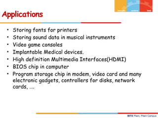
BITS Pilani, PilaniCampus
• Storing fonts for printers
• Storing sound data in musical instruments
• Video game consoles
• Implantable Medical devices.
• High definition Multimedia Interfaces(HDMI)
• BIOS chip in computer
• Program storage chip in modem, video card and many
electronic gadgets, controllers for disks, network
cards, ….
Applications
11.
BITS Pilani, PilaniCampus
CPU places address A and then read control signal on
the memory bus
Memory Read Operation (1)
Load operation: MOV R4, A
R4 [A]
ALU
Register file
Bus interface
A
0
A
x
Main memory
I/O bridge
R4
12.
BITS Pilani, PilaniCampus
Main memory reads A from the memory bus, retrieves
word x, and places it on the bus
Memory Read Operation (2)
Load operation: MOV R4, A
R4 [A]
ALU
Register file
Bus interface
x 0
A
x
Main
memory
R4
I/O bridge
13.
BITS Pilani, PilaniCampus
CPU read word x from the bus and copies it into
register R4.
Memory Read Operation (3)
x
ALU
Register file
Bus interface x
Main memory
0
A
R4
I/O bridge
Load operation: MOV R4, A
R4 [A]
14.
BITS Pilani, PilaniCampus
CPU places address A and WRITE control signal on bus.
Main memory reads them and waits for the
corresponding data word to arrive.
Memory Write Operation (1)
Load operation: MOV A, R4
[A] R4
y
ALU
Register file
Bus interface
A
Main memory
0
A
R4
I/O bridge
15.
BITS Pilani, PilaniCampus
CPU places data word y on the bus
Memory Write Operation (2)
y
ALU
Register file
Bus interface
y
Main memory
0
A
R4
I/O bridge
Load operation: MOV A, R4
[A] R4
16.
BITS Pilani, PilaniCampus
Main memory reads data word y from the bus and
stores it at address A.
Memory Write Operation (3)
y
ALU
Register file
Bus interface y
main memory
0
A
R4
I/O bridge
Load operation: MOV A, R4
[A] R4
17.
BITS Pilani, PilaniCampus
SDR Single Data Rate
DDR Double Data Rate
SDR Vs DDR
Clk
Data
Clk
Data
SDR
DDR
18.
BITS Pilani, PilaniCampus
Construct 1K X4 bit memory using 1Kx1 bit chip
Typical Memory Connection
Examples
CE
D3 D0
D1
D2
R / W
C3
1K x 1
C1
1K x 1
C0
1K x 1
C2
1K x 1
Address Bus – A9 - A0
19.
BITS Pilani, PilaniCampus
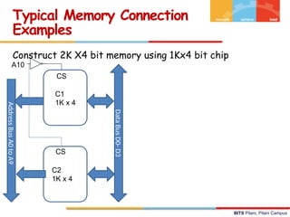
Construct 2K X4 bit memory using 1Kx4 bit chip
Typical Memory Connection
Examples
C1
1K x 4
C2
1K x 4
Data
Bus
D0-
D3
Address
Bus
A0
to
A9
A10
CS
CS
20.
BITS Pilani, PilaniCampus
• Hard Failure
– Caused by harsh environmental abuse or
manufacturing defects or wear
– Memory cell is permanently stuck at 0 or 1
– Permanent defect
• Soft Error
– Random, non-destructive
– alters the contents of one or more memory cells
without damaging the memory.
– No permanent damage to memory
– Caused by power supply problems
• Detected using Hamming error correcting code
Error Correction
BITS Pilani, PilaniCampus
• The comparison logic receives two K-bit values -
Computed check bits and check bits in the message. A
bit-by-bit exclusive-OR is done on the two inputs. The
result is called the Syndrome word.
• The comparison yields one of three results
1. No errors are detected.
2. An error is detected and it is possible to correct the
error
3. An error is detected but it is not possible to correct
it.
Error Correcting Code Function
23.
BITS Pilani, PilaniCampus
• What should be the length of the code K ?
• Result of comparison is known as syndrome word
• length of the syndrome word is K bits, Length of Data
is “M” bits
• Length of K should satisfy 2K
-1 >= M+K
• For 8 bit data(i.e. M is 8 )
• K = 1, 21
– 1 >= 8 + 1
• K = 2, 22
– 1 >= 8 + 2
3 >= 10
• K = 3, 23
– 1 >= 8 + 3
7 >= 11
• K = 4, 24
– 1 >= 8 + 4
15 >= 12 If M = 8, then K is 4
Hamming Code…..
24.
BITS Pilani, PilaniCampus
• Generate 4-bit syndrome for an 8 bit data word with
following characteristics
– If the syndrome contains all 0’s, no error has been
detected.
– If the syndrome contains one and only one bit set
to one, then an error has occurred in one of the 4
check bits. No correction is needed
– If the syndrome contains more than one bit set to
1, then the numerical value of the syndrome
indicates the position of the data bit in error. This
data bit is inverted to correction
Hamming code….
25.
BITS Pilani, PilaniCampus
Truth Table of XOR
⊕
A B A B
⊕
0 0 0
0 1 1
1 0 1
1 1 0
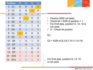
Layout of Data and Check bits
Bit
position 12 11 10 9 8 7 6 5 4 3 2 1
Position
Number
1100 1011 1010 1001 1000 0111 0110 0101 0100 0011 0010 0001
Data bit D8 D7 D6 D5 C4 D4 D3 D2 C3 D1 C2 C1
Dn : Data bits, Cn : Check bits
26.
BITS Pilani, PilaniCampus
Position C4 C3 C2 C1
1 C1 0 0 0 1
2 C2 0 0 1 0
3 D1 0 0 1 1
4 C3 0 1 0 0
5 D2 0 1 0 1
6 D3 0 1 1 0
7 D4 0 1 1 1
8 C4 1 0 0 0
9 D5 1 0 0 1
10 D6 1 0 1 0
11 D7 1 0 1 1
12 D8 1 1 0 0
13 D9 1 1 0 1
14 D10 1 1 1 0
15 D11 1 1 1 1
• Position 0000 not listed
• Check bit = XOR of position = 1
• For 8 bit data, position13, 14, 15 is
not used.
• 2n
: Check bit position
Ex:
C2 = XOR of (2,3,6,7,10,11,14,15)
For 8 bit data, position13, 14, 15
is not used
27.
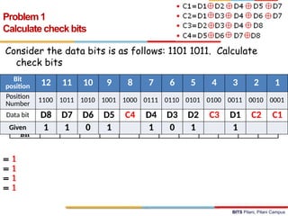
BITS Pilani, PilaniCampus
Consider the data bits is as follows: 1101 1011. Calculate
check bits
Problem 1
Calculate check bits
Bit
position 12 11 10 9 8 7 6 5 4 3 2 1
Position
Number
1100 1011 1010 1001 1000 0111 0110 0101 0100 0011 0010 0001
Data bit D8 D7 D6 D5 C4 D4 D3 D2 C3 D1 C2 C1
Given 1 1 0 1 1 0 1 1
= 1
= 1
= 1
= 1
28.
BITS Pilani, PilaniCampus
Consider the data + code k is as follows: 1101 0101 1101
Find out if there is an error. If so which bit is having
error and what is the actual data.
Problem 2
29.
BITS Pilani, PilaniCampus
Problem 2 - Solution
Bit
position 12 11 10 9 8 7 6 5 4 3 2 1
Position
Number 1100 1011 1010 1001 1000 0111 0110 0101 0100 0011 0010 0001
Data bit D8 D7 D6 D5 C4 D4 D3 D2 C3 D1 C2 C1
Received 1 1 0 1 0 1 0 1 1 1 0 1
Consider the data + code k is as follows: 1101 0101 1101
Find out if there is an error. If so which bit is having
error and what is the actual data.
30.
BITS Pilani, PilaniCampus
Problem 2 – solution…
Bit
position 12 11 10 9 8 7 6 5 4 3 2 1
Position
Number 1100 1011 1010 1001 1000 0111 0110 0101 0100 0011 0010 0001
Data bit D8 D7 D6 D5 C4 D4 D3 D2 C3 D1 C2 C1
Received 1 1 0 1 0 1 0 1 1 1 0 1
Calculate C1
= 1
Consider the data + code k is as follows: 1101 0101 1101
Find out if there is an error. If so which bit is having
error and what is the actual data.
31.
BITS Pilani, PilaniCampus
Problem 2 – solution…
Bit
position 12 11 10 9 8 7 6 5 4 3 2 1
Position
Number
1100 1011 1010 1001 1000 0111 0110 0101 0100 0011 0010 0001
Data bit D8 D7 D6 D5 C4 D4 D3 D2 C3 D1 C2 C1
Received 1 1 0 1 0 1 0 1 1 1 0 1
Calculate C2
Consider the data + code k is as follows: 1101 0101 1101
Find out if there is an error. If so which bit is having
error and what is the actual data.
= 1
32.
BITS Pilani, PilaniCampus
Problem 2 – solution…
Bit
position 12 11 10 9 8 7 6 5 4 3 2 1
Position
Number
1100 1011 1010 1001 1000 0111 0110 0101 0100 0011 0010 0001
Data bit D8 D7 D6 D5 C4 D4 D3 D2 C3 D1 C2 C1
Received 1 1 0 1 0 1 0 1 1 1 0 1
Calculate C3
Consider the data + code k is as follows: 1101 0101 1101
Find out if there is an error. If so which bit is having
error and what is the actual data.
= 1
33.
BITS Pilani, PilaniCampus
Problem 2 – solution…
Bit
position 12 11 10 9 8 7 6 5 4 3 2 1
Position
Number
1100 1011 1010 1001 1000 0111 0110 0101 0100 0011 0010 0001
Data bit D8 D7 D6 D5 C4 D4 D3 D2 C3 D1 C2 C1
Received 1 1 0 1 0 1 0 1 1 1 0 1
Calculate C4
Consider the data + code k is as follows: 1101 0101 1101
Find out if there is an error. If so which bit is having
error and what is the actual data.
= 1
34.
BITS Pilani, PilaniCampus
Problems 2 – solution…
Bit
position 12 11 10 9 8 7 6 5 4 3 2 1
Position
Number
1100 1011 1010 1001 1000 0111 0110 0101 0100 0011 0010 0001
Data bit D8 D7 D6 D5 C4 D4 D3 D2 C3 D1 C2 C1
Received 1 1 0 1 0 1 0 1 1 1 0 1
Computed value of C4 C3 C2 C1 : 1 1 1 1
In message : 0 1 0 1
-----------------------------------------------------------
XOR to find error bit position: 1 0 1 0 => (10)10
-----------------------------------------------------------
Toggle the 10th
bit position(i.e. D6) in the given data
Correct message is 1111 0101 1101
Consider the data + code k is as follows: 1101 0101 1101
Find out if there is an error. If so which bit is having
error and what is the actual data.
35.
BITS Pilani, PilaniCampus
Data : 10101100 (M = 8)
Compute Check Bits
Problem 3
Bit
position 12 11 10 9 8 7 6 5 4 3 2 1
Position
Number
1100 1011 1010 1001 1000 0111 0110 0101 0100 0011 0010 0001
Data bit D8 D7 D6 D5 D4 D3 D2 D1
Check bit C4 C3 C2 C1
1 0 1 0 ? 1 1 0 ? 0 ? ?
36.
BITS Pilani, PilaniCampus
• Magnetic Disk
– RAID
– Removable
• Optical
– CD-ROM
– CD-Recordable (CD-R)
– CD-R/W
– DVD
• Magnetic Tape
Types of External Memory
37.
BITS Pilani, PilaniCampus
Magnetic Disk Drive
Spindle
Arm
Actuator
Platters
Electronics
(including a
processor
and memory!)
SCSI
connector
Image courtesy of Seagate Technology
38.
BITS Pilani, PilaniCampus
• Disks consist of
platters, each with
two surfaces.
• Each surface consists
of concentric rings
called tracks
• Aligned tracks form a
cylinder
• Each track consists of
sectors separated by
gaps.
Disk Geometry
Surface 0
Surface 1
Surface 2
Surface 3
Surface 4
Surface 5
Cylinder k
Spindle
Platter 0
Platter 1
Platter 2
Spindle
Surface
Tracks
Track k
Sectors
Gaps
39.
BITS Pilani, PilaniCampus
• Capacity: maximum number of bits that can be stored.
– Vendors express capacity in units of gigabytes (GB
/TB), where 1 GB = 230
Bytes, 1 TB = 240
Bytes,
• Capacity is determined by these technology factors:
– Recording density (bits/in): number of bits that
can be squeezed into a 1 inch segment of a track.
– Track density (tracks/in): number of tracks that
can be squeezed into a 1 inch radial segment.
– Areal density (bits/in2): product of recording and
track density.
Disk Capacity
40.
BITS Pilani, PilaniCampus
• Modern disks partition tracks into
disjoint subsets called recording
zones
– Each track in a zone has the
same number of sectors,
determined by the
circumference of innermost
track.
– Each zone has a different
number of sectors/track,
outer zones have more
sectors/track than inner
zones.
– So we use average number of
sectors/track when computing
capacity.
Recording zones
41.
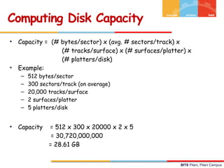
BITS Pilani, PilaniCampus
• Capacity = (# bytes/sector) x (avg. # sectors/track) x
(# tracks/surface) x (# surfaces/platter) x
(# platters/disk)
• Example:
– 512 bytes/sector
– 300 sectors/track (on average)
– 20,000 tracks/surface
– 2 surfaces/platter
– 5 platters/disk
• Capacity = 512 x 300 x 20000 x 2 x 5
= 30,720,000,000
= 28.61 GB
Computing Disk Capacity
42.
BITS Pilani, PilaniCampus
Disk Operation (Single-Platter View)
The disk
surface
spins at a fixed
rotational rate
By moving radially, the arm
can position the read/write
head over any track.
The read/write head
is attached to the end
of the arm and flies over
the disk surface on
a thin cushion of air.
spindle
spindle
spindle
spindle
spindle
43.
BITS Pilani, PilaniCampus
Disk Operation (Multi-Platter View)
Arm
Read/write heads
move in unison
from cylinder to cylinder
Spindle
44.
BITS Pilani, PilaniCampus
Disk Access
Need to access a sector
colored in blue
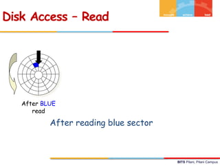
BITS Pilani, PilaniCampus
Disk Access – Read
After BLUE
read
After reading blue sector
49.
BITS Pilani, PilaniCampus
Disk Access – Read
After BLUE
read
Red request scheduled next
50.
BITS Pilani, PilaniCampus
Disk Access – Seek
After BLUE
read
Seek for RED
Seek to red’s track
Disk Access – Seek
51.
BITS Pilani, PilaniCampus
Disk Access – Rotational Latency
After BLUE
read
Seek for RED Rotational latency
Wait for red sector to rotate around
52.
BITS Pilani, PilaniCampus
Disk Access – Read
After BLUE
read
Seek for RED Rotational latency After RED read
Complete read of red
53.
BITS Pilani, PilaniCampus
Disk Access – Access Time Components
After BLUE
read
Seek for RED Rotational latency After RED read
Data transfer Seek Rotational
latency
Data transfer
Editor's Notes
#6 1 k x 8 bits memory organization needs to be explained.
#7 Begin with types of semiconductor memory : ROM and RAM
#11 Explain the operation with respect to the load operation
#13 At the end summarize the read operation.
A MAR Address Bus
Read Control Bus
Memory reads the data from the memory location data bus
Data bus MDR
MDR R4 resister
#15 R4 MBR
A MAR Address Bus
Write Signal Control Bus
Memory reads the address and Control signal
MDR Data bus
Data bus Memory
#16 R4 MBR
A MAR Address Bus
Write Signal Control Bus
Memory reads the address and Control signal
MDR Data bus
Data bus Memory
#17 Most desktops and notebooks use one of several popular types of dynamic random access memory (DRAM) for the main system memory.
Single data rate (SDR) SDRAM is the older type of memory, commonly used in computers prior to 2002.
Double data rate (DDR) SDRAM hit the mainstream computer market around 2002 and is a straightforward evolution from SDR SDRAM. The most significant difference between DDR and SDR is that DDR reads data on both the rising and falling edges of the clock signal, enabling a DDR memory module to transfer data twice as fast as an SDR memory module.
Systems implementing the follow up technology to DDR, called DDR2, began to appear in mid-2004. DDR2 achieves speeds beyond that of DDR, delivering bandwidth of up to 8.5 GB per second. Frequently, DDR2-based systems can use memory installed in pairs to run in "dual channel mode" to increase memory throughput even further.
DDR3, DDR4 and DDR5 represent further improvements in memory technology, with improvements in bandwidth as well as power consumption, leading to better performance and stability as time went on and the standards evolved.
Generally speaking, motherboards are built to support only one type of memory. You cannot mix and match SDRAM, DDR, DDR2, DDR3, DDR4, or DDR5 memory on the same motherboard in any system. They will not function and will not even fit in the same sockets.
The right type of memory to use is the one that your computer is compatible with
#20 Alpha Particle: a helium nucleus emitted by some radioactive substances, originally regarded as a ray.
==============
A semiconductor memory system is subject to errors. These can be categorized as
hard failures and soft errors. A hard failure is a permanent physical defect so that the
memory cell or cells affected cannot reliably store data but become stuck at 0 or 1 or switch erratically between 0 and 1. Hard errors can be caused by harsh environmental
abuse, manufacturing defects, and wear. A soft error is a random, nondestructive
event that alters the contents of one or more memory cells without damaging the
memory. Soft errors can be caused by power supply problems or alpha particles.
These particles result from radioactive decay and are distressingly common because
radioactive nuclei are found in small quantities in nearly all materials. Both hard and
soft errors are clearly undesirable, and most modern main memory systems include
logic for both detecting and correcting errors.
#21 Figure 5.7 illustrates in general terms how the process is carried out. When
data are to be read into memory, a calculation, depicted as a function f, is performed
on the data to produce a code. Both the code and the data are stored. Thus, if an
M-bit word of data is to be stored and the code is of length K bits, then the actual
size of the stored word is M Kbits.
#41 Divide the number by 1024x1024x1024
Clearly mention to students that 1 G is not 10^9 but it is 2^30 = 1024x1024x1024


![BITS Pilani, Pilani Campus
CPU places address A and then read control signal on
the memory bus
Memory Read Operation (1)
Load operation: MOV R4, A
R4 [A]
ALU
Register file
Bus interface
A
0
A
x
Main memory
I/O bridge
R4](https://image.slidesharecdn.com/cosscontactsession02-251220232332-5a06d7b2/85/Computer_Organization_Contact_Session_02-pptx-11-320.jpg)
![BITS Pilani, Pilani Campus
Main memory reads A from the memory bus, retrieves
word x, and places it on the bus
Memory Read Operation (2)
Load operation: MOV R4, A
R4 [A]
ALU
Register file
Bus interface
x 0
A
x
Main
memory
R4
I/O bridge](https://image.slidesharecdn.com/cosscontactsession02-251220232332-5a06d7b2/85/Computer_Organization_Contact_Session_02-pptx-12-320.jpg)
![BITS Pilani, Pilani Campus
CPU read word x from the bus and copies it into
register R4.
Memory Read Operation (3)
x
ALU
Register file
Bus interface x
Main memory
0
A
R4
I/O bridge
Load operation: MOV R4, A
R4 [A]](https://image.slidesharecdn.com/cosscontactsession02-251220232332-5a06d7b2/85/Computer_Organization_Contact_Session_02-pptx-13-320.jpg)
![BITS Pilani, Pilani Campus
CPU places address A and WRITE control signal on bus.
Main memory reads them and waits for the
corresponding data word to arrive.
Memory Write Operation (1)
Load operation: MOV A, R4
[A] R4
y
ALU
Register file
Bus interface
A
Main memory
0
A
R4
I/O bridge](https://image.slidesharecdn.com/cosscontactsession02-251220232332-5a06d7b2/85/Computer_Organization_Contact_Session_02-pptx-14-320.jpg)
![BITS Pilani, Pilani Campus
CPU places data word y on the bus
Memory Write Operation (2)
y
ALU
Register file
Bus interface
y
Main memory
0
A
R4
I/O bridge
Load operation: MOV A, R4
[A] R4](https://image.slidesharecdn.com/cosscontactsession02-251220232332-5a06d7b2/85/Computer_Organization_Contact_Session_02-pptx-15-320.jpg)
![BITS Pilani, Pilani Campus
Main memory reads data word y from the bus and
stores it at address A.
Memory Write Operation (3)
y
ALU
Register file
Bus interface y
main memory
0
A
R4
I/O bridge
Load operation: MOV A, R4
[A] R4](https://image.slidesharecdn.com/cosscontactsession02-251220232332-5a06d7b2/85/Computer_Organization_Contact_Session_02-pptx-16-320.jpg)