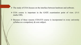
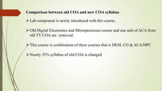
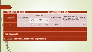
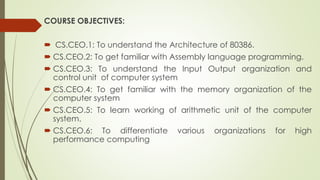
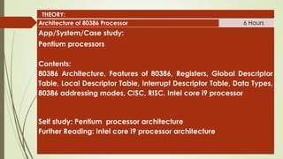
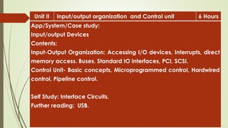
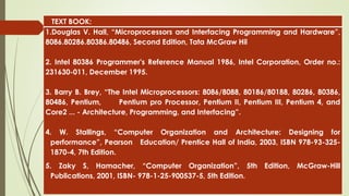
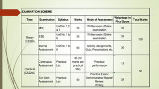
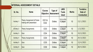
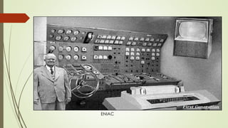
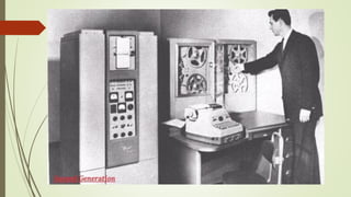
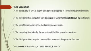
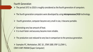
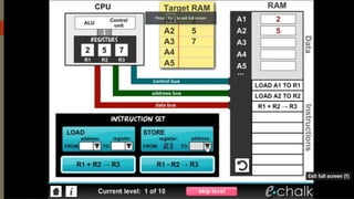
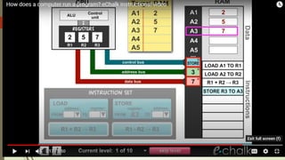
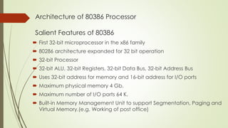
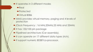
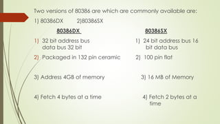
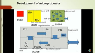
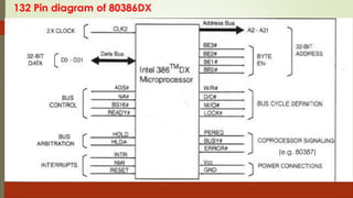
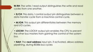
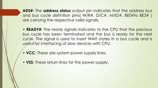
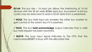
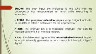
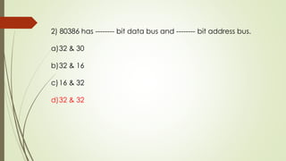
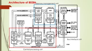
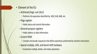
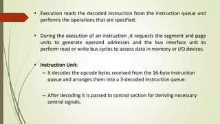
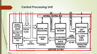
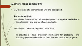
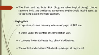
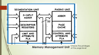
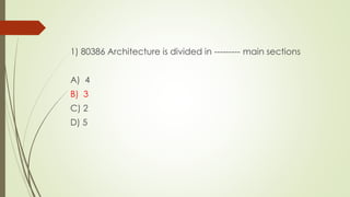
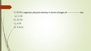
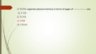
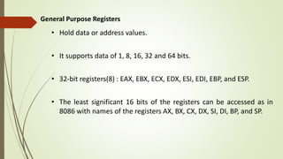
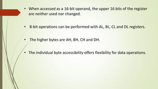
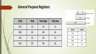
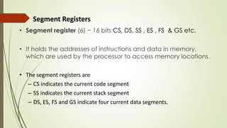
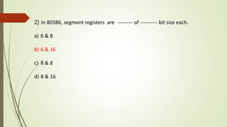
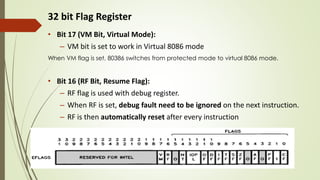
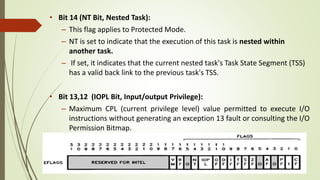
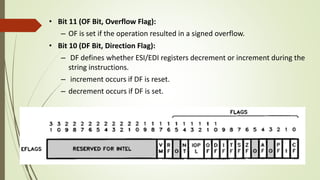
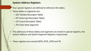
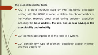
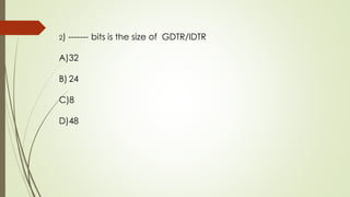
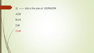
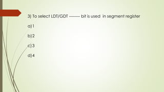
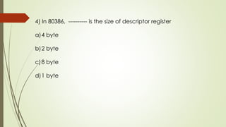
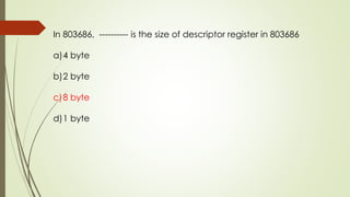
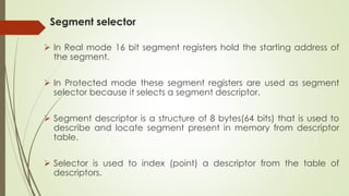
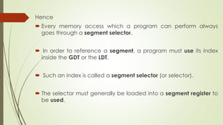
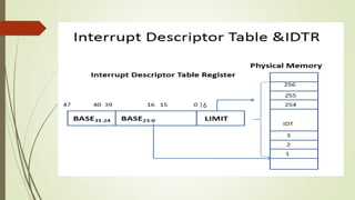
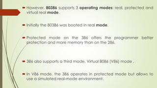
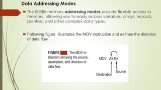
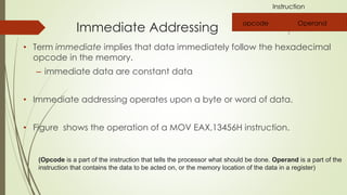
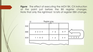
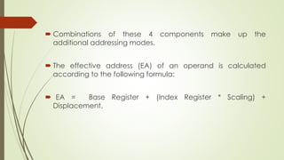
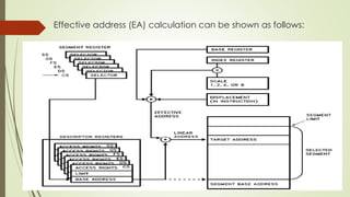
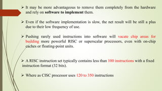
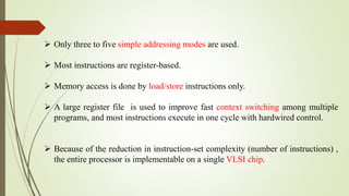
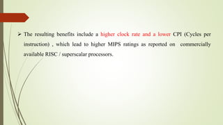
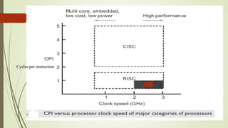
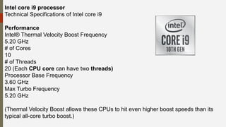
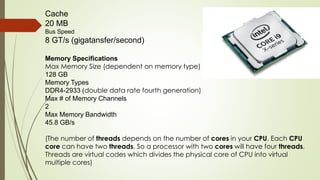
The document outlines the importance of the Computer Organization and Architecture (COA) course, describing its relevance in everyday applications and its foundational role in computer science. It details the course structure, including units focused on microprocessor architecture, input/output organization, memory systems, and arithmetic operations, as well as teaching and evaluation schemes. Additionally, the document provides historical context for computer generations and introduces various microprocessors, particularly the 80386, emphasizing its architecture and capabilities.


![Figure The operation of the MOV AL,[1234H] instruction
when DS=10000H .
• This instruction transfers a copy contents of memory location 11234H
into AL.
– the effective address is formed by adding
1234H (the offset address) and 10000H](https://image.slidesharecdn.com/coauniti-241010164456-e21022fd/85/Computer-Organisation-and-Architecture-Unit-I-pdf-167-320.jpg)
![Figure 4 The operation of the MOV AX,[BX] instruction when BX =
1000H and DS = 0100H. Note that this instruction is shown after the
contents of memory are transferred to AX.
(100*10)](https://image.slidesharecdn.com/coauniti-241010164456-e21022fd/85/Computer-Organisation-and-Architecture-Unit-I-pdf-170-320.jpg)
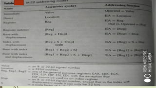
![• Figure 6 shows how data are addressed by the
MOV DX,[BX + DI] instruction when the microprocessor operates
in the real mode.
• The Intel assembler requires this addressing mode appear as
[BX][DI] instead of [BX + DI].
• The MOV DX,[BX + DI] instruction is MOV DX,[BX][DI] for a
program written for the Intel ASM assembler.](https://image.slidesharecdn.com/coauniti-241010164456-e21022fd/85/Computer-Organisation-and-Architecture-Unit-I-pdf-172-320.jpg)
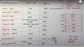
![Figure An example showing how the base-plus-index addressing
mode functions for the MOV DX,[BX + DI] instruction.
Notice that memory address 02010H is accessed because DS=0100H,
BX=1000H and DI=0010H.](https://image.slidesharecdn.com/coauniti-241010164456-e21022fd/85/Computer-Organisation-and-Architecture-Unit-I-pdf-173-320.jpg)


![COA_UNIT-1new[1].pdf](https://cdn.slidesharecdn.com/ss_thumbnails/coaunit-1new1-230919072310-a464b1d1-thumbnail.jpg?width=640&height=640&fit=bounds)