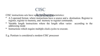
Introduction: CISC
• CISCmeans Complex Instruction Set Computer chips that are easy to program and which make
efficient use of memory. Since the earliest machines were programmed in assembly language and
memory was slow and expensive, the CISC philosophy was commonly implemented in large
computers as the PDP-11 and the DECsystem 10 and 20 machines.
• Most common microprocessor designs such as the Intel 80x86 and Motorola 68K series
followed the CISC philosophy.
• CISC was developed to make compiler development simpler. It shifts most of the burden of generating
machine instructions to the processor.
• For example, instead of having to make a compiler write long machine instructions to calculate a
square-root, a CISC processor would have a built-in ability to do this.
4.
CISC
Attributes
CISC instructions setshave some common characteristics:
• A 2-operand format, where instructions have a source and a destination. Register to
register, register to memory, and memory to register commands.
• Variable length instructions where the length often varies according to the
addressing mode
• Instructions which require multiple clock cycles to execute.
E.g. Pentium is considered a modern CISC processor
5.
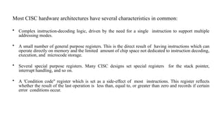
Most CISC hardwarearchitectures have several characteristics in common:
• Complex instruction-decoding logic, driven by the need for a single instruction to support multiple
addressing modes.
• A small number of general purpose registers. This is the direct result of having instructions which can
operate directly on memory and the limited amount of chip space not dedicated to instruction decoding,
execution, and microcode storage.
• Several special purpose registers. Many CISC designs set special registers for the stack pointer,
interrupt handling, and so on.
• A 'Condition code" register which is set as a side-effect of most instructions. This register reflects
whether the result of the last operation is less than, equal to, or greater than zero and records if certain
error conditions occur.
6.
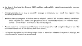
At the timeof their initial development, CISC machines used available technologies to optimize computer
performance.
• Microprogramniing is as easy as assembly language to implement, and much less expensive than
hardwiring a control unit.
• The ease of microcoding new instructions allowed designers to make CISC machines upwardly compatible:
a new computer could run the same programs as earlier computers because the new computer would
contain a superset of the instructions of the earlier computers.
• As each instruction became more capable, fewer instructions could be used to implement a given task. This
made more efficient use of the relatively slow main memory.
• Because microprogram instruction sets can be written to match the constructs of high-level languages, the
compiler does not have to be as complicated.
7.
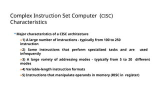
Complex Instruction SetComputer (CISC)
Characteristics
Major characteristics of a CISC architecture
»1) A large number of instructions - typically from 100 to 250
instruction
»2) Some instructions that perform specialized tasks and are used
infrequently
»3) A large variety of addressing modes - typically from 5 to 20 different
modes
»4) Variable-length instruction formats
»5) Instructions that manipulate operands in memory (RISC in register)
8.
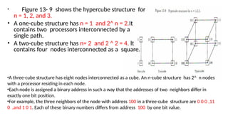
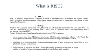
What is RISC?
•RISC?
RISC, or Reduced Instruction Set Computer. is a type of microprocessor architecture that utilizes a small,
highly-optimized set of instructions, rather than a more specialized set of instructions often found in other
types of architectures.
• History
The first RISC projects came from IBM, Stanford, and UC-Berkeley in the late 70s and early 80s. The
IBM 801, Stanford MIPS, and Berkeley RISC 1 and 2 were all designed with a similar philosophy which
has become known as RISC.
Certain design features have been characteristic of most RISC processors:
– one cycle execution time: RISC processors have a CPI (clock per instruction) of one cycle. This is due
to the optimization of each instruction on the CPU and a technique called PIPELINING
– pipelining: a techique that allows for simultaneous execution of parts, or stages, of instructions to more
efficiently process instructions;
– large number of registers: the RISC design philosophy generally incorporates a larger
number of registers to prevent in large amounts of interactions with memory
9.
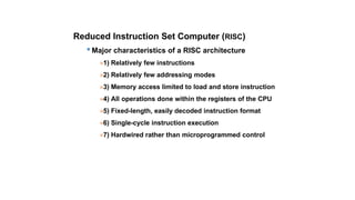
Reduced Instruction SetComputer (RISC)
Major characteristics of a RISC architecture
»1) Relatively few instructions
»2) Relatively few addressing modes
»3) Memory access limited to load and store instruction
»4) All operations done within the registers of the CPU
»5) Fixed-length, easily decoded instruction format
»6) Single-cycle instruction execution
»7) Hardwired rather than microprogrammed control
10.
– RISC Instruction
•Only use LOAD and STORE instruction when communicating between memory and
CPU
• All other instructions are executed within the registers of the CPU without referring to
memory
Program to evaluate X = ( A + B ) * ( C + D )
LOAD R1, A R1 M [ A]
LOAD R2, B R2 M [B]
LOAD R3, C R3 M [C]
LOAD R4, D R4 M [D]
ADD R1, R1, R2 R1 R1 R2
ADD R3, R3, R4 R3 R3 R4
MUL R1, R1, R3 R1 R1 R3
STORE X, R1 M [ X ] R1
•Load instruction transfers the operand from memory to CPU
Register.
•Add and Multiply operations are executed with data in the registers
without accessing the memory.
•Result is then stored in the memory with store information.
11.
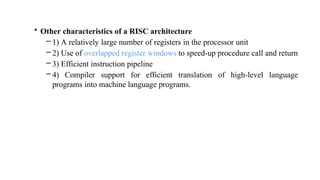
• Other characteristicsof a RISC architecture
– 1) A relatively large number of registers in the processor unit
– 2) Use of overlapped register windows to speed-up procedure call and return
– 3) Efficient instruction pipeline
– 4) Compiler support for efficient translation of high-level language
programs into machine language programs.
12.
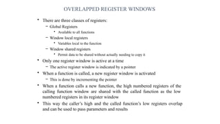
OVERLAPPED REGISTER WINDOWS
•There are three classes of registers:
– Global Registers
• Available to all functions
– Window local registers
• Variables local to the function
– Window shared registers
• Permit data to be shared without actually needing to copy it
• Only one register window is active at a time
– The active register window is indicated by a pointer
• When a function is called, a new register window is activated
– This is done by incrementing the pointer
• When a function calls a new function, the high numbered registers of the
calling function window are shared with the called function as the low
numbered registers in its register window
• This way the caller’s high and the called function’s low registers overlap
and can be used to pass parameters and results
13.
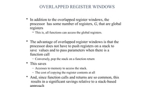
OVERLAPPED REGISTER WINDOWS
•In addition to the overlapped register windows, the
processor has some number of registers, G, that are global
registers
– This is, all functions can access the global registers.
• The advantage of overlapped register windows is that the
processor does not have to push registers on a stack to
save values and to pass parameters when there is a
function call
– Conversely, pop the stack on a function return
• This saves
– Accesses to memory to access the stack.
– The cost of copying the register contents at all
• And, since function calls and returns are so common, this
results in a significant savings relative to a stack-based
approach
14.
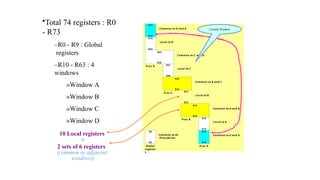
R15
R10
R73
R64
R63
R58
R57
R48
R47
R42
R41
R32
R31
R26
R15
R10
R25
R16
Common to Dand A
Local to D
Common to C and D
Local to C
Common to B and C
Local to B
Common to A and B
Local to A
Common to A and D
R9
R0
Common to all
Procedures
Global
register
s
Proc A
Proc B
Proc C
Proc D
Circular Window
10 Local registers
+
2 sets of 6 registers
(common to adjacent
windows)
•Total 74 registers : R0
- R73
–R0 - R9 : Global
registers
–R10 - R63 : 4
windows
»Window A
»Window B
»Window C
»Window D
15.
• Example) ProcedureA calls procedure B
– R26 - R31
» Store parameters for procedure B
» Store results of procedure B
– R16 - R25 : Local to procedure A
– R32 - R41 : Local to procedure B
• Window Size = L + 2C + G = 10 + ( 2 X 6 ) + 10 = 32 registers
• Register File (total register) = (L + C) X W + G = (10 + 6 ) X 4 + 10 = 74 registers
– G : Global registers = 10
L : Local registers = 10
C : Common registers = 6
W : Number of windows = 4
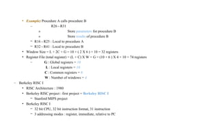
– Berkeley RISC I
• RISC Architecture : 1980
• Berkeley RISC project : first project = Berkeley RISC I
– Stanford MIPS project
• Berkeley RISC I
– 32 bit CPU, 32 bit instruction format, 31 instruction
– 3 addressing modes : register, immediate, relative to PC
16.
Instruction Set: Tab. 8-12
Instruction Format : Fig. 8-10
Register Mode : bit 13 = 0
» S2 = register
» Example) ADD R22, R21, R23
ADD Rs, S2, Rd : Rd = Rs + S2
Register Immediate Mode : bit 13 = 1
» S2 = sign extended 13 bit
constant
» Example) LDL (R22)#150, R5
LDL (Rs)S2, Rd : Rd =
M[R22] + 150
PC Relative Mode
» Y = 19 bit relative address
» Example) JMPR COND, Y
Jump to PC = PC + Y
» CWP (Current Window
Pointer)
CALL, RET?stack pointer ?????
RISC Architecture
Originator
S2
5
Not used
8
Rs
5
Rd
5
0
5 4
1 4 1 3 1 2
0
1
19 1 8
3 1 2 4 2 3
Op co d e
8
(a) Register m o d e : (S2 specifies a register)
S2
1 3
Rs
5
Rd
5
0
1 9 18 1 4 1 3 1 2
1
1
3 1 24 2 3
Opco de
8
(b) Register-immediate m o d e : (S2 specifies an operand)
0
3 1 2 4 2 3 19 1 8
Op co de COND
Y
8 5
1 9
(c) PC relative m o d e :
Architecture Originator Licensees
Alpha D E C Mitsubishi, Samsung
MIPS MIPS Technologies NEC, Toshiba
PA-RISC Hewlett Packard Hitachi, Samsung
PowerPC Apple, IBM, Motorola Bul
Sparc Sun Fujitsu, Hyundai
i960 Intel Intel only (Embedded Controler)
17.
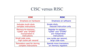
CISC versus RISC
CISCRISC
Emphasis on hardware Emphasis on software
Includes multi-clock
complex instructions
Single-clock,
reduced instruction only
Memory-to-memory:
"LOAD" and "STORE"
incorporated in
instructions
Register to register:
"LOAD" and "STORE"
are independent
instructions
Small code sizes,
high cycles per second
Low cycles per second,
large code sizes
Transistors used for storing
complex instructions
Spends more transistors
on memory registers
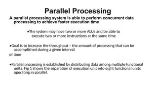
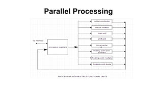
Parallel Processing
A parallelprocessing system is able to perform concurrent data
processing to achieve faster execution time
•The system may have two or more ALUs and be able to
execute two or more instructions at the same time
•Goal is to increase the throughput – the amount of processing that can be
accomplished during a given interval
of time
•Parallel processing is established by distributing data among multiple functional
units. Fig 1 shows the separation of execution unit into eight functional units
operating in parallel.
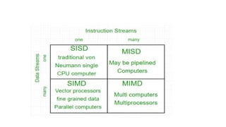
Flynn’s Taxonomy
There arevariety of ways parallel processing can be classified.
Parallel processing occuring in instruction stream/data stream or both.
Flynn’s classification divides computer into four major groups as
follows:
Single instruction stream, single data stream – SISD
Single instruction stream, multiple data stream – SIMD
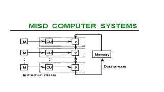
Multiple instruction stream, single data stream – MISD
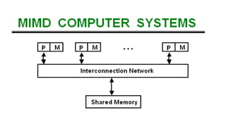
Multiple instruction stream, multiple data stream – MIMD
23.
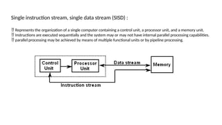
Single instruction stream,single data stream (SISD) :
Represents the organization of a single computer containing a control unit, a processor unit, and a memory unit.
Instructions are executed sequentially and the system may or may not have internal parallel processing capabilities.
parallel processing may be achieved by means of multiple functional units or by pipeline processing.
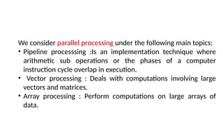
We consider parallelprocessing under the following main topics:
• Pipeline processsing :Is an implementation technique where
arithmetic sub operations or the phases of a computer
instruction cycle overlap in execution.
• Vector processing : Deals with computations involving large
vectors and matrices.
• Array processing : Perform computations on large arrays of
data.
28.
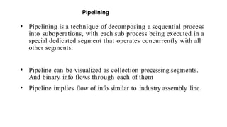
Pipelining
• Pipelining isa technique of decomposing a sequential process
into suboperations, with each sub process being executed in a
special dedicated segment that operates concurrently with all
other segments.
• Pipeline can be visualized as collection processing segments.
And binary info flows through each of them
• Pipeline implies flow of info similar to industry assembly line.
29.
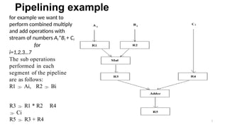
Pipelining example
for examplewe want to
perform combined multiply
and add operations with
stream of numbers Ai*Bi + Ci
for
i=1,2,3…7
The sub operations
performed in each
segment of the pipeline
are as follows:
R1 Ai, R2 Bi
R3 R1 * R2 R4
Ci
R5 R3 + R4 7
30.
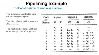
Pipelining example
Content ofregisters of pipelining example
•The five registers are loaded with
new data every clock pulse.
•The effect of each clock is shown in
table as shown
•The clock must continue until last
output emerges out of the pipeline.
31.
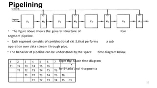
Pipelining
• The figureabove shows the general structure of four
segment pipeline.
• Each segment consists of combinational ckt Si that performs a sub
operation over data stream through pipe.
• The behavior of pipeline can be understood by the space time diagram below.
Refer the space time diagram
for 6-tasks and 4 segments
1 2 3 4 5 6 7 8 9
T1 T2 T3 T4 T5 T6 •
T1 T2 T3 T4 T5 T6
T1 T2 T3 T4 T5 T6
T1 T2 T3 T4 T5 T6
31
32.
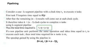
Pipelining
Consider a case: k-segment pipeline with a clock time tp to execute n tasks
First task T1requires time equal to Ktp
After that the remaining (n - 1) results will come out at each clock cycle.
It therefore takes k + (n - 1) clock cycles to complete n tasks
using k-segment pipeline
Thus the total time required is:
If a non pipeline unit performs the same operation and takes time equal to tn to
execute each task ; then total time required for n tasks is ntn
The speedup gained by using the pipeline is:
S= ntn / (k + n - 1)tp
33.
Now consider nonpipeline unit that performs the same operation
and takes time equal to tn to complete each task.
Total time required is ntn.
The speedup ration is given as:
35.
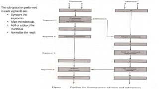
Arithmetic Pipeline
• Pipelinearithmetic units are usually found in very high speed computers.
• They are used to implement floating point operations.
• We will now discuss the pipeline unit for the floating point addition and
subtraction.
• The inputs to floating point adder pipeline are two normalized floating point
numbers.
• A and B are mantissas and a and b are the exponents.
• The floating point addition and subtraction can be performed in four segments.
36.
The sub-operation performed
ineach segments are:
• Compare the
exponents
• Align the mantissas
• Add or subtract the
mantissas
• Normalize the result
37.
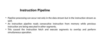
Instruction Pipeline
• Pipelineprocessing can occur not only in the data stream but in the instruction stream as
well.
• An instruction pipeline reads consecutive instruction from memory while previous
instruction are being executed in other segments.
• This caused the instruction fetch and execute segments to overlap and perform
simultaneous operation.
38.
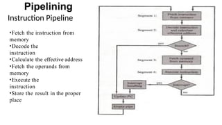
Pipelining
Instruction Pipeline
•Fetch theinstruction from
memory
•Decode the
instruction
•Calculate the effective address
•Fetch the operands from
memory
•Execute the
instruction
•Store the result in the proper
place
39.
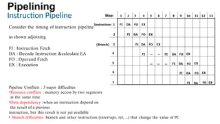
Pipelining
Instruction Pipeline
Consider thetiming of instruction pipeline
as shown adjoining
FI : Instruction Fetch
DA : Decode Instruction &calculate EA
FO : Operand Fetch
EX : Execution
Pipeline Conflicts : 3 major difficulties
•Resource conflicts : memory access by two segments
at the same time
•Data dependency :when an instruction depend on
the result of a previous
instruction, but this result is not yet available
• Branch difficulties :branch and other instruction (interrupt, ret, ..) that change the value of PC
40.
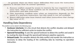
Handling Data Dependency
Thisproblem can be solved in the following ways:
• Hardware interlocks: It is the circuit that detects the conflict situation and delayed
the instruction by sufficient cycles to resolve the conflict.
• Operand Forwarding: It uses the special hardware to detect the conflict and avoid it
by routing the data through the special path between pipeline segments.
• Delayed Loads: The compiler detects the data conflict and reorder the instruction as
necessary to delay the loading of the conflicting data by inserting no operation
instruction.
41.
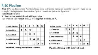
RISC Pipeline
RISC CPUhas Instruction Pipeline ;Single-cycle instruction execution Compiler support Here for an
example 3 Suboperations Instruction Cycle is considered ( show in fig) where
I : Instruction fetch
A : Instruction decoded and ALU operation
E : Transfer the output of ALU to a register, memory, or PC
42.
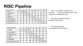
RISC Pipeline
• Thereare several techniques for
reducing branch penalties one of the
method is of delayed branch
• The above fig shows using no
operation instruction ;
• The below fig shows
rearranging the instructions
43.
Vector Processing
Computers withvector processing capabilities are in demand in specialized applications. The
following are representative application areas where vector processing is of the utmost importance.
•Long-range weather forecasting
•Petroleum explorations
•Seismic data analysis
•Medical diagnosis
•Aerodvnamics and space flight simulations
•Artificial intelligence and expert systems
•Mapping the human genome
•Image processing
• Many scientific problems require arithmetic operations on large arrays of numbers.
• These numbers are usually formulated as vectors and matrices of floating-point numbers.
• A vector is an ordered set of a one-dimensional array of data items.
• The element Vi of vector V is written as V(I) and the index I refers to a memory address or register
where the number is stored.
• A vector V of length n is represented as a row vector by
V = [V1 V2 V3 •• Vn ]
44.
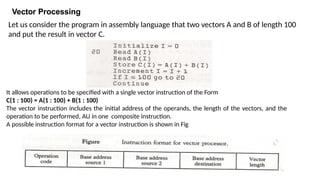
Vector Processing
It allowsoperations to be specified with a single vector instruction of the Form
C(1 : 100) = A(1 : 100) + B(1 : 100)
The vector instruction includes the initial address of the operands, the length of the vectors, and the
operation to be performed, AU in one composite instruction.
A possible instruction format for a vector instruction is shown in Fig
Let us consider the program in assembly language that two vectors A and B of length 100
and put the result in vector C.
45.
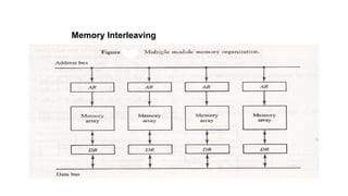
Vector Processing
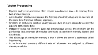
• Pipelineand vector processors often require simultaneous access to memory from
two or more sources.
• An instruction pipeline may require the fetching of an instruction and an operand at
the same time from two different segments.
• Similarly, an arithmetic pipeline usually requires two or more operands to enter the
pipeline at the same time.
• Instead of using two memory buses for simultaneous access, the memory can be
partitioned into a number of modules connected to a common memory address and
data buses.
• The advantage of a modular memory is that it allows the use of a technique called
interleaving.
• In an interleaved memory, different sets of addresses are assigned to different
memory modules.
This requires threemultiplication and(after initializing c11 to 0) three addition.
Total number of addition or multiplication required is 3*9.
In general inner product consists of the sum of k product terms of the form:
In typical application value of k may be 100 or even 1000.
The inner product calculation on a pipeline vector processor is shown below.
Floating point adder and multiplier are assumed to have four segments each.
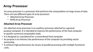
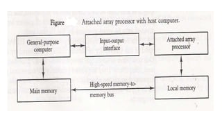
Array Processor
An arrayprocessor is a processor that performs the computations on large arrays of data.
There are two different types of array processor:
• Attached Array Processor
• SIMD Array Processor
Attached Array Processor
• It is designed as a peripheral for a conventional host computer.
• Its purpose is to enhance the performance of the computer by providing vector
processing.
• It achieves high performance by means of parallel processing with multiple functional
units.
•An attached array processor is an auxiliary processor attached to a general-
purpose computer. It is intended to improve the performance of the host computer
in specific numerical computation tasks.
52.
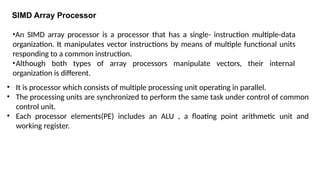
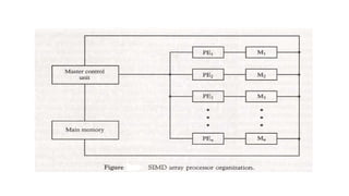
SIMD Array Processor
•It is processor which consists of multiple processing unit operating in parallel.
• The processing units are synchronized to perform the same task under control of common
control unit.
• Each processor elements(PE) includes an ALU , a floating point arithmetic unit and
working register.
•An SIMD array processor is a processor that has a single- instruction multiple-data
organization. It manipulates vector instructions by means of multiple functional units
responding to a common instruction.
•Although both types of array processors manipulate vectors, their internal
organization is different.
54.
MULTI PROCESSORS
• Characteristicsof multi processors
• Interconnection of Structures
• Inter processor Arbitration
• Inter processor Communication and Synchronization
• Cache Coherence
55.
• A multiprocessorsystem is an interconnection of two or more
CPUs with memory and input— output equipment. The term
“processor” in multiprocessor can mean either a central
processing unit (CPU) or an input—output processor (lOP).
• As it is most commonly defined, a multiprocessor system
implies the existence of multiple CPUs, although usually there
will be one or more IOPs as well.
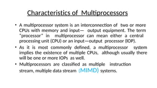
• Multiprocessors are classified as multiple instruction
stream, multiple data stream (MIMD) systems.
Characteristics of Multiprocessors
56.
• There aresome similarities between Multiprocessor and
Multicomputer systems since both support concurrent
operations.
• However, there exists important distinction between a system
with multiple computers and a system with multiple
processors.
• Computers are interconnected with each other means of
communication lines to form a computer network.
• The network consists of several autonomous computers
that may or may not communicate with each other.
• A multiprocessor system is controlled by one operating system
that provides interaction between processors and all the
components of the system cooperate in the solution of a
problem.
57.
• Multiprocessing improvesthe reliability of the system so that a
failure or error in one part has a limited effect on the rest of the
system.
• If a fault causes one processor to fail, a second
processor can be assigned to perform the functions
of the disabled processor.
• The system as a whole can continue to function correctly with
perhaps some loss in efficiency.
• The benefit derived from a multiprocessor organization is an
improved system performance.
• The system derives its high performance from the fact that
computations can proceed in parallel in one of two ways.
• 1. Multiple independent jobs can be made to operate in parallel.
• 2. A single job can be partitioned into multiple parallel tasks.
58.
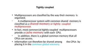
Tightly coupled
• Multiprocessorsare classified by the way their memory is
organized.
• A multiprocessor system with common shared memory is
classified as a shared-memory or tightly coupled
multiprocessor.
• In fact, most commercial tightly coupled multiprocessors
provide a cache memory with each CPU.
• in addition, there is a global common memory that all
CPUs can access.
• Information can therefore be shared among the CPUs by
placing it in the common global memory.
59.
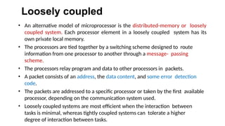
Loosely coupled
• Analternative model of microprocessor is the distributed-memory or loosely
coupled system. Each processor element in a loosely coupled system has its
own private local memory.
• The processors are tied together by a switching scheme designed to route
information from one processor to another through a message- passing
scheme.
• The processors relay program and data to other processors in packets.
• A packet consists of an address, the data content, and some error detection
code.
• The packets are addressed to a specific processor or taken by the first available
processor, depending on the communication system used.
• Loosely coupled systems are most efficient when the interaction between
tasks is minimal, whereas tightly coupled systems can tolerate a higher
degree of interaction between tasks.
60.
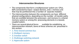
Interconnection Structures
• Thecomponents that form a multiprocessor system are CPUs,
lOPs connected to input—output devices, and a memory unit
that may be partitioned into a number of separate modules.
• The interconnection between the components can have different
physical configurations, depending on the number of transfer paths
that are available between the processors and memory in a shared
memory system or among the processing elements in a loosely
coupled system.
• There are several physical forms available for establishing an
interconnection network, Some of these schemes are presented in
this section:
• 1. Time-shared common bus
• 2, Multiport memory
• 3. Crossbar switch
• 4. Multistage switching network
• 5. Hypercube system
61.
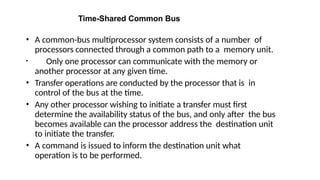
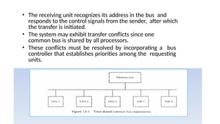
Time-Shared Common Bus
•A common-bus multiprocessor system consists of a number of
processors connected through a common path to a memory unit.
• Only one processor can communicate with the memory or
another processor at any given time.
• Transfer operations are conducted by the processor that is in
control of the bus at the time.
• Any other processor wishing to initiate a transfer must first
determine the availability status of the bus, and only after the bus
becomes available can the processor address the destination unit
to initiate the transfer.
• A command is issued to inform the destination unit what
operation is to be performed.
62.
• The receivingunit recognizes its address in the bus and
responds to the control signals from the sender, after which
the transfer is initiated.
• The system may exhibit transfer conflicts since one
common bus is shared by all processors.
• These conflicts must be resolved by incorporating a bus
controller that establishes priorities among the requesting
units.
63.
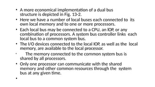
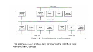
• A moreeconomical implementation of a dual bus
structure is depicted in Fig. 13-2.
• Here we have a number of local buses each connected to its
own local memory and to one or more processors.
• Each local bus may be connected to a CPU, an lOP, or any
combination of processors. A system bus controller links each
local bus to a common system bus.
• The I/O devices connected to the local IOP, as well as the local
memory, are available to the local processor.
• The memory connected to the common system bus is
shared by all processors.
• Only one processor can communicate with the shared
memory and other common resources through the system
bus at any given time.
•
64.
•The other processorsare kept busy communicating with their local
memory and I/O devices.
65.
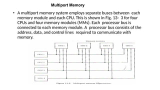
Multiport Memory
• Amultiport memory system employs separate buses between each
memory module and each CPU. This is shown in Fig. 13- 3 for four
CPUs and four memory modules (MMs). Each processor bus is
connected to each memory module. A processor bus consists of the
address, data, and control lines required to communicate with
memory.
66.
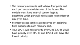
• The memorymodule is said to have four ports and
each port accommodates one of the buses. The
module must have internal control logic to
determine which port will have access to memory at
any given time.
• Memory access conflicts are resolved by assigning
fixed priorities to each memory port.
• Thus CPU 1 will have priority over CPU 2, CPU 2 will
have priority over CPU 3, and CPU 4 will have the
lowest priority.
67.
• The advantageof the multiport memory
organization is the high transfer rate that can be
achieved because of the multiple paths between
processors and memory.
• The disadvantage is that it requires expensive
memory control logic and a large number of
cables and connectors.
• As a consequences this interconnection structure
is usually appropriate for systems with a small
number of processors.
68.
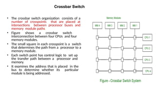
Crossbar Switch
• Thecrossbar switch organization consists of a
number of crosspoints that are placed at
intersections between processor buses and
memory module paths.
• Figure shows a crossbar switch
interconnection between four CPUs and four
memory modules.
• The small square in each crosspoint is a switch
that determines the path from a processor to a
memory module.
• Each switch point has control logic to set up
the transfer path between a processor and
memory.
• It examines the address that is placed in the
bus to determine whether its particular
module is being addressed.
69.
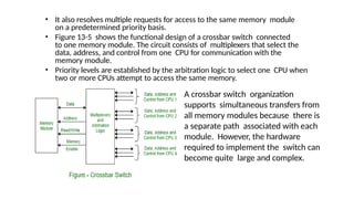
• It alsoresolves multiple requests for access to the same memory module
on a predetermined priority basis.
• Figure 13-5 shows the functional design of a crossbar switch connected
to one memory module. The circuit consists of multiplexers that select the
data, address, and control from one CPU for communication with the
memory module.
• Priority levels are established by the arbitration logic to select one CPU when
two or more CPUs attempt to access the same memory.
A crossbar switch organization
supports simultaneous transfers from
all memory modules because there is
a separate path associated with each
module. However, the hardware
required to implement the switch can
become quite large and complex.
70.
Multistage switching Network
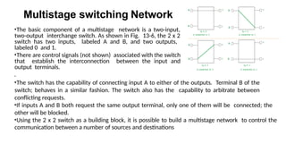
•Thebasic component of a multistage network is a two-input,
two-output interchange switch. As shown in Fig. 13-6, the 2 x 2
switch has two inputs, labeled A and B, and two outputs,
labeled 0 and 1.
•There are control signals (not shown) associated with the switch
that establish the interconnection between the input and
output terminals.
.
•The switch has the capability of connecting input A to either of the outputs. Terminal B of the
switch; behaves in a similar fashion. The switch also has the capability to arbitrate between
conflicting requests.
•If inputs A and B both request the same output terminal, only one of them will be connected; the
other will be blocked.
•Using the 2 x 2 switch as a building block, it is possible to build a multistage network to control the
communication between a number of sources and destinations
71.
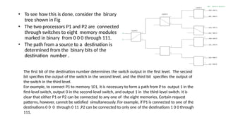
• To seehow this is done, consider the binary
tree shown in Fig
• The two processors P1 and P2 are connected
through switches to eight memory modules
marked in binary from 0 0 0 through 111.
• The path from a source to a destination is
determined from the binary bits of the
destination number .
The first bit of the destination number determines the switch output in the first level. The second
bit specifies the output of the switch in the second level, and the third bit specifies the output of
the switch in the third level.
For example, to connect P1 to memory 101, it is necessary to form a path from P to output 1 in the
first-level switch, output 0 in the second-level switch, and output 1 in the third-level switch. It is
clear that either P1 or P2 can be connected to any one of the eight memories, Certain request
patterns, however, cannot be satisfied simultaneously. For example, if P1 is connected to one of the
destinations 0 0 0 through 0 11 ,P2 can be connected to only one of the destinations 1 0 0 through
111.
72.
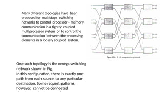
Many different topologieshave been
proposed for multistage switching
networks to control processor—memory
communication in a tightly coupled
multiprocessor system or to control the
communication between the processing
elements in a loosely coupled system.
One such topology is the omega switching
network shown in Fig.
In this configuration, there is exactly one
path from each source to any particular
destination. Some request patterns,
however, cannot be connected
73.
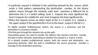
• A particularrequest is initiated in the switching network by the source, which
sends a 3-bit pattern representing the destination number. As the binary
pattern moves through the network, each level examines a different bit to
determine the 2 x 2 switch setting. Level 1 inspects the most significant bit,
level 2 inspects the middle bit, and level 3 inspects the least significant bit.
• When the request arrives on either input of the 2 x 2 switch, it is routed a
the upper output if the specified bit is 0 or to the lower output if the bit is 1.
•In tightly coupled multiprocessor system, the source is a processor and the
destination is a memory module.
•The first pass through the network sets up the path.
•Succeeding passes are used to transfer the address into memory and then transfer
the data in either direction, depending on whether the request is a read or a write.
•In a loosely coupled multiprocessor system, both the source and destination are
processing elements. After the path is established, the source processor transfers a
message to the destination processor.
74.
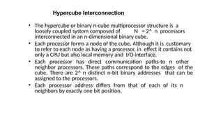
Hypercube Interconnection
• Thehypercube or binary n-cube multiprocessor structure is a
loosely coupled system composed of N = 2^ n processors
interconnected in an n-dimensional binary cube.
• Each processor forms a node of the cube. Although it is customary
to refer to each node as having a processor, in effect it contains not
only a CPU but also local memory and I/O interface.
• Each processor has direct communication paths-to n other
neighbor processors. These paths correspond to the edges of the
cube. There are 2^ n distinct n-bit binary addresses that can be
assigned to the processors.
• Each processor address differs from that of each of its n
neighbors by exactly one bit position.
75.
• Figure 13-9 shows the hypercube structure for
n = 1, 2, and 3.
• A one-cube structure has n = 1 and 2^ n = 2.It
contains two processors interconnected by a
single path.
• A two-cube structure has n= 2 and 2 ^ 2 = 4. lt
contains four nodes interconnected as a square.
•A three-cube structure has eight nodes interconnected as a cube. An n-cube structure has 2^ n nodes
with a processor residing in each node.
•Each node is assigned a binary address in such a way that the addresses of two neighbors differ in
exactly one bit position.
•For example, the three neighbors of the node with address 100 in a three-cube structure are 0 0 0 ,11
0 ,and 1 0 1. Each of these binary numbers differs from address 100 by one bit value.
76.
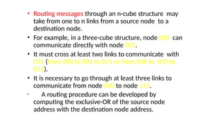
• Routing messagesthrough an n-cube structure may
take from one to n links from a source node to a
destination node.
• For example, in a three-cube structure, node 000 can
communicate directly with node 001.
• It must cross at least two links to communicate with
011 (from 000 to 001 to 011 or from 000 to 010 to
011).
• It is necessary to go through at least three links to
communicate from node 000 to node 111.
• A routing procedure can be developed by
computing the exclusive-OR of the source node
address with the destination node address.
77.
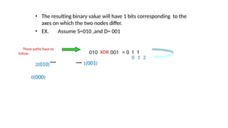
• The resultingbinary value will have 1 bits corresponding to the
axes on which the two nodes differ.
• EX. Assume S=010 ,and D= 001
0 1 2
1(001)
010 XOR 001 = 0 1 1
These paths have to
follow
2(010)
0(000)
78.
• The followingexample illustrates the use of a deterministic
routing technique in a hypercube network.
• Example : Assume that S =S5S4 . . . S1S0 to be the source node address, and that D = D5D4 . . .
D1D0 is the destination node address in a six-dimensional hypercube message passing system. Let R
= S XOR D be the exclusive OR function executed bitwise for
each node in the path.
• Consider the case whereby S = 10(001010) and D = 39(100111).
The order in which these dimensions are traversed is not important. Let us
assume that the message will follow the route by traversing the following
dimensions 5, 3, 2, and 0. Then the route is totally determined as:
10 (001010) 42(101010) 34(100010) 38(100110) 39 (100111).
001010 XOR 100111 =1 0 1 1 0 1
0 2 3 5
These pathes have to follow
source destination
79.
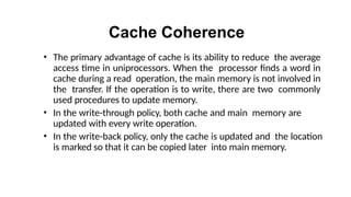
Cache Coherence
• Theprimary advantage of cache is its ability to reduce the average
access time in uniprocessors. When the processor finds a word in
cache during a read operation, the main memory is not involved in
the transfer. If the operation is to write, there are two commonly
used procedures to update memory.
• In the write-through policy, both cache and main memory are
updated with every write operation.
• In the write-back policy, only the cache is updated and the location
is marked so that it can be copied later into main memory.
80.
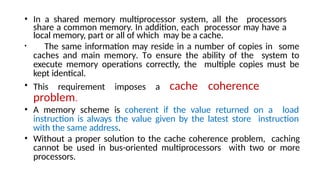
• In ashared memory multiprocessor system, all the processors
share a common memory. In addition, each processor may have a
local memory, part or all of which may be a cache.
• The same information may reside in a number of copies in some
caches and main memory. To ensure the ability of the system to
execute memory operations correctly, the multiple copies must be
kept identical.
• This requirement imposes a cache coherence
problem.
• A memory scheme is coherent if the value returned on a load
instruction is always the value given by the latest store instruction
with the same address.
• Without a proper solution to the cache coherence problem, caching
cannot be used in bus-oriented multiprocessors with two or more
processors.
81.
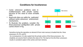
Conditions for Incoherence
•Cache coherence problems exist in
multiprocessors with private caches
because of the need to share writable
data.
• Read-only data can safely be replicated
without cache coherence enforcement
mechanisms.
• To illustrate the problem, consider the
three-processor configration with private
caches shown in Fig.
Sometime during the operation an element X from main memory is loaded into the three
processors, P1, P2, and P3.
As a consequence, it is also copied into the private caches of the three processors. For
simplicity, we assume that X contains the value of 52. The load on X to the three processors
results in consistent copies in the caches and main memory.
82.
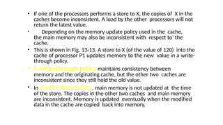
• If oneof the processors performs a store to X, the copies of X in the
caches become inconsistent. A load by the other processors will not
return the latest value.
• Depending on the memory update policy used in the cache,
the main memory may also be inconsistent with respect to’ the
cache.
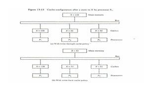
• This is shown in Fig. 13-13. A store to X (of the value of 120) into the
cache of processor P1 updates memory to the new value in a write-
through policy.
• A write-through policy maintains consistency between
memory and the originating cache, but the other two caches are
inconsistent since they still hold the old value.
• In a write-back policy, main memory is not updated at the time
of the store. The copies in the other two caches and main memory
are inconsistent. Memory is updated eventually when the modified
data in the cache are copied back into memory.
84.
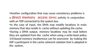
•Another configuration thatmay cause consistency problems is
a direct memory access (DMA) activity in conjunction
with an TOP connected to the system bus.
•In the case of input, the DMA may modify locations in main
memory that also reside in cache without updating the cache.
•During a DMA output, memory locations may be read before
they are updated from the cache when using a write-back policy.
1/0-based memory incoherence can he overcome by making the
IOP a participant in the cache coherent solution that is adopted in
the system.
85.
Solutions to theCache Coherence Problem
• A simple scheme is to disallow private caches for each processor and have a shared
cache memory associated with main memory.
• Every data access is made to the shared cache.
• This method violates the principle of closeness of Cpu to cache and increases the
average memory access time.
• In effect, this scheme solves the problem by avoiding it.
• For performance considerations it is desirable to attach a private cache to each
processor.
• One scheme that has been used allows only nonshared and read-only data to be
stored in caches. Such items are called Cachable.
• Shared writable data are noncachable.
• The compiler must tag data as either cachable or noncachable, and the system
hardware makes sure that only cachable data are stored in caches.
• The noncachable data remain in main memory.
86.
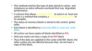
• This methodrestricts the type of data stored in caches and
introduces an extra software overhead that may degradate
performance.
• A scheme that allows writable data to exist in at least one
cache is a method that employs a centralized global table in
its compiler.
• The status of memory blocks is stored in the central global
table.
• Each block is identified as read-only (RO) or read and write
(RW).
• All caches can have copies of blocks identified as RO.
• Only one cache can have a copy of an RW block.
• Thus if the data are updated in the cache with RW block, the
other caches are not affected because they do not have a
copy of this block.
87.
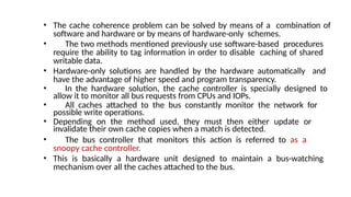
• The cachecoherence problem can be solved by means of a combination of
software and hardware or by means of hardware-only schemes.
• The two methods mentioned previously use software-based procedures
require the ability to tag information in order to disable caching of shared
writable data.
• Hardware-only solutions are handled by the hardware automatically and
have the advantage of higher speed and program transparency.
• In the hardware solution, the cache controller is specially designed to
allow it to monitor all bus requests from CPUs and IOPs.
• All caches attached to the bus constantly monitor the network for
possible write operations.
• Depending on the method used, they must then either update or
invalidate their own cache copies when a match is detected.
• The bus controller that monitors this action is referred to as a
snoopy cache controller.
• This is basically a hardware unit designed to maintain a bus-watching
mechanism over all the caches attached to the bus.
88.
• Various schemeshave been proposed to solve the cache coherence problem
by means of snoopy cache protocol.
• The simplest method is to adopt a write-through policy and use the following
procedure.
• All the snoopy controllers watch the bus for memory store
operations.
• When a word in a cache is updated by writing into it, the
corresponding location in main memory is also updated.
• The local snoopy controllers in all other caches check their memory to
determine if they have a copy of the word that has been overwritten.
• If a copy exists in a remote cache, that location is marked invalid.
• Because all caches snoop on all bus writes, whenever a word is written, the
net effect is to update it in the original cache and main memory and remove
it from all other caches.
• If at some future time a processor accesses the invalid item from its
cache, the response is equivalent to a cache miss, and the updated item is
transferred from main memory.
• In this case inconsistent versions are prevented.
89.
Hardware Solution: SnoopingCache
• Widely used in bus-based multiprocessors.
• The cache controller constantly watches the bus.
• Write Invalidate
• When a processor writes into C, all copies of it in
• other processors are invalidated. These processors
• have to read a valid copy either from M, or from the
• processor that modified the variable.
• Write Broadcast
• Instead of invalidating, why not broadcast the updated
• value to the other processors sharing that copy?
• This will act as write through for shared data, and
• write back for private data.
• Write broadcast consumes more bus bandwidth
compared to write invalidate. Why?
90.
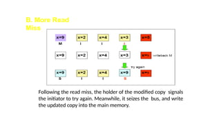
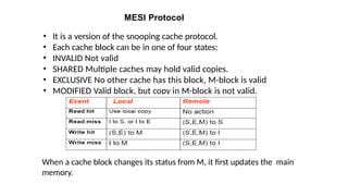
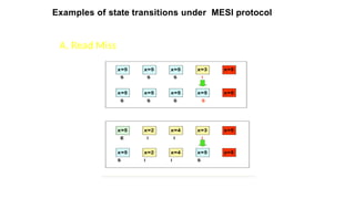
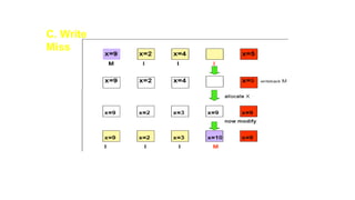
MESI Protocol
• Itis a version of the snooping cache protocol.
• Each cache block can be in one of four states:
• INVALID Not valid
• SHARED Multiple caches may hold valid copies.
• EXCLUSIVE No other cache has this block, M-block is valid
• MODIFIED Valid block, but copy in M-block is not valid.
When a cache block changes its status from M, it first updates the main
memory.
B. More Read
Miss
Followingthe read miss, the holder of the modified copy signals
the initiator to try again. Meanwhile, it seizes the bus, and write
the updated copy into the main memory.
• The cachecoherence problem can be solved by means of a combination of
software and hardware or by means of hardware-only schemes.
• The two methods mentioned previously use software-based procedures
require the ability to tag information in order to disable caching of shared
writable data.
• Hardware-only solutions are handled by the hardware automatically and have
the advantage of higher speed and program transparency.
• In the hardware solution, the cache controller is specially designed to allow
it to monitor all bus requests from CPUs and IOPs.
• All caches attached to the bus constantly monitor the network for
possible write operations.
• Depending on the method used, they must then either update or invalidate
their own cache copies when a match is detected.
• The bus controller that monitors this action is referred to as a
snoopy cache controller.
• This is basically a hardware unit designed to maintain a bus-watching
mechanism over all the caches attached to the bus.
95.
• Various schemeshave been proposed to solve the cache coherence problem
by means of snoopy cache protocol.
• The simplest method is to adopt a write-through policy and use the following
procedure.
• All the snoopy controllers watch the bus for memory store
operations.
• When a word in a cache is updated by writing into it, the
corresponding location in main memory is also updated.
• The local snoopy controllers in all other caches check their memory to
determine if they have a copy of the word that has been overwritten.
• If a copy exists in a remote cache, that location is marked invalid.
• Because all caches snoop on all bus writes, whenever a word is written, the
net effect is to update it in the original cache and main memory and remove
it from all other caches.
• If at some future time a processor accesses the invalid item from its
cache, the response is equivalent to a cache miss, and the updated item is
transferred from main memory.
• In this case inconsistent versions are prevented.
96.
Hardware Solution: SnoopingCache
• Widely used in bus-based multiprocessors.
• The cache controller constantly watches the bus.
• Write Invalidate
• When a processor writes into C, all copies of it in
• other processors are invalidated. These processors
• have to read a valid copy either from M, or from the
• processor that modified the variable.
• Write Broadcast
• Instead of invalidating, why not broadcast the updated
• value to the other processors sharing that copy?
• This will act as write through for shared data, and
• write back for private data.
• Write broadcast consumes more bus bandwidth
compared to write invalidate. Why?
97.
MESI Protocol
• Itis a version of the snooping cache protocol.
• Each cache block can be in one of four states:
• INVALID Not valid
• SHARED Multiple caches may hold valid copies.
• EXCLUSIVE No other cache has this block, M-block is valid
• MODIFIED Valid block, but copy in M-block is not valid.
When a cache block changes its status from M, it first updates the main
memory.
B. More Read
Miss
Followingthe read miss, the holder of the modified copy signals
the initiator to try again. Meanwhile, it seizes the bus, and write
the updated copy into the main memory.

![– RISC Instruction
• Only use LOAD and STORE instruction when communicating between memory and
CPU
• All other instructions are executed within the registers of the CPU without referring to
memory
Program to evaluate X = ( A + B ) * ( C + D )
LOAD R1, A R1 M [ A]
LOAD R2, B R2 M [B]
LOAD R3, C R3 M [C]
LOAD R4, D R4 M [D]
ADD R1, R1, R2 R1 R1 R2
ADD R3, R3, R4 R3 R3 R4
MUL R1, R1, R3 R1 R1 R3
STORE X, R1 M [ X ] R1
•Load instruction transfers the operand from memory to CPU
Register.
•Add and Multiply operations are executed with data in the registers
without accessing the memory.
•Result is then stored in the memory with store information.](https://image.slidesharecdn.com/coaunit5-250829113424-e12091fc/85/COA-Computer-Organization-and-Architecture-10-320.jpg)
![ Instruction Set : Tab. 8-12
Instruction Format : Fig. 8-10
Register Mode : bit 13 = 0
» S2 = register
» Example) ADD R22, R21, R23
ADD Rs, S2, Rd : Rd = Rs + S2
Register Immediate Mode : bit 13 = 1
» S2 = sign extended 13 bit
constant
» Example) LDL (R22)#150, R5
LDL (Rs)S2, Rd : Rd =
M[R22] + 150
PC Relative Mode
» Y = 19 bit relative address
» Example) JMPR COND, Y
Jump to PC = PC + Y
» CWP (Current Window
Pointer)
CALL, RET?stack pointer ?????
RISC Architecture
Originator
S2
5
Not used
8
Rs
5
Rd
5
0
5 4
1 4 1 3 1 2
0
1
19 1 8
3 1 2 4 2 3
Op co d e
8
(a) Register m o d e : (S2 specifies a register)
S2
1 3
Rs
5
Rd
5
0
1 9 18 1 4 1 3 1 2
1
1
3 1 24 2 3
Opco de
8
(b) Register-immediate m o d e : (S2 specifies an operand)
0
3 1 2 4 2 3 19 1 8
Op co de COND
Y
8 5
1 9
(c) PC relative m o d e :
Architecture Originator Licensees
Alpha D E C Mitsubishi, Samsung
MIPS MIPS Technologies NEC, Toshiba
PA-RISC Hewlett Packard Hitachi, Samsung
PowerPC Apple, IBM, Motorola Bul
Sparc Sun Fujitsu, Hyundai
i960 Intel Intel only (Embedded Controler)](https://image.slidesharecdn.com/coaunit5-250829113424-e12091fc/85/COA-Computer-Organization-and-Architecture-16-320.jpg)


![Vector Processing
Computers with vector processing capabilities are in demand in specialized applications. The
following are representative application areas where vector processing is of the utmost importance.
•Long-range weather forecasting
•Petroleum explorations
•Seismic data analysis
•Medical diagnosis
•Aerodvnamics and space flight simulations
•Artificial intelligence and expert systems
•Mapping the human genome
•Image processing
• Many scientific problems require arithmetic operations on large arrays of numbers.
• These numbers are usually formulated as vectors and matrices of floating-point numbers.
• A vector is an ordered set of a one-dimensional array of data items.
• The element Vi of vector V is written as V(I) and the index I refers to a memory address or register
where the number is stored.
• A vector V of length n is represented as a row vector by
V = [V1 V2 V3 •• Vn ]](https://image.slidesharecdn.com/coaunit5-250829113424-e12091fc/85/COA-Computer-Organization-and-Architecture-43-320.jpg)