The document summarizes research on chemical vapor deposition of ruthenium thin films using tricarbonyl(1,3-cyclohexadiene)Ru(0) as the precursor. Key findings include:
(1) NMR analysis showed the likely decomposition reaction is (C6H8)Ru(CO)3 → H2 + C6H6 + 3CO, with a low activation energy of 17 ± 7 kJ/mol, enabling low-temperature deposition.
(2) Films were crystalline at all deposition temperatures and exhibited a compact microstructure. Texture was determined by growth conditions rather than thermodynamic driving forces.
(3) Contrary to surface science studies, the 1,3
The document discusses a presentation by Safe Harbor regarding forward-looking statements and includes risk factors. It also provides an overview of China Gerui including its revenues, earnings, market capitalization, industry position, investment highlights, value chain, defining its niche market, revenue by industry application, economics of its business model, and out pacing competition. China Gerui is a leading Chinese processor of specialty cold-rolled steel known for its customized, high-margin products.
This document provides an overview and rationale for subscribing to the IPO of Electrosteel Steels. Key points include:
Electrosteel Steels is setting up a 2.2 million tonne greenfield steel plant costing Rs. 7,362 crores to be financed with a 3:1 debt to equity ratio. Commercial production is expected to start in phases from October 2010. The company has raw material linkages through agreements with Electrosteel Castings mines and will benefit from technical tie-ups and a strategic alliance with Stemcor for marketing. The IPO is recommended for long-term investors given the progressive commissioning of the new plant and factors supporting margins.
Chemical vapor deposition of manganese nitrideteresaspicer
The document summarizes research on the chemical vapor deposition of manganese nitride thin films using bis[di(tert-butyl)amido]manganese(II) as a precursor. Key findings include:
1) The reaction of the precursor with ammonia is very facile, allowing for manganese nitride film growth at temperatures as low as 80°C.
2) Films of the phase η-Mn3N2 can be deposited in crystalline form even at these low temperatures, attributed to the lability of high-spin Mn(II).
3) A transamination reaction mechanism between the precursor and ammonia is proposed, analogous to other transition metal precursors.
(1) Doctoral research focused on developing novel chemical vapor deposition (CVD) processes for depositing thin films by designing new precursor molecules.
(2) CVD is commonly used to deposit thin films in integrated circuits but traditional high-temperature CVD can lead to non-uniform coatings, especially in small features.
(3) By designing precursors that react at lower temperatures or have lower sticking probabilities, more uniform coatings can be achieved without compromising film growth rates. Key findings showed how purposeful ligand and co-reactant design influenced precursor reactivity and stability.
Cristina talks about capacitors that can last longer at high temperatures are extreme humidity. In this case, when there is no moisture or too much moisture. This presentation covers the technology innovations applied to a high-reliability polymer tantalum capacitor.
IRJET- Quality Improvement of Ductile Iron Casting by Thermal AnalysisIRJET Journal
The document discusses using thermal analysis to improve the quality of ductile iron castings by reducing shrinkage defects. It presents the results of an experiment where cooling curves were recorded for ductile iron castings with different section thicknesses. Nine castings were produced with variations in chemical composition, inoculation amount, and pouring temperature. The cooling curves were analyzed to understand the solidification behavior and identify conditions that led to shrinkage. The results showed that thermal analysis is effective for controlling melt quality in ductile iron and avoiding shrinkage, with nil undercooling indicating sufficient inoculation for a given composition and thickness.
IRJET- Simulation of High K Dielectric MOS with HFo2 as a Gate DielectricIRJET Journal
This document discusses the simulation of a MOSFET device using HfO2 as the high-k gate dielectric material. It begins with an introduction to the need for high-k dielectrics to replace silicon dioxide as traditional MOSFETs continue to scale down. HfO2 is identified as a promising high-k material due to its high dielectric constant. The document then outlines the process steps to simulate an HfO2-based MOSFET using Silvaco simulation software. Key steps include depositing an HfO2 layer, doping the source and drain, and depositing metal contacts. A comparison is made between traditional MOSFETs and high-k MOSFETs, showing
The document discusses advanced ceramic substrates for microelectronic systems. It describes desired substrate properties such as high electrical resistivity and thermal conductivity. It also discusses common ceramic materials used as substrates like silicon carbide and aluminum nitride and their fabrication methods. The document outlines the definitions, thermal, mechanical, and electrical properties to consider for ceramic substrates. It also covers metallization techniques for ceramic substrates, such as thick film and thin film processes.
Analysis of Lead-free Perovskite solar cellsIRJET Journal
This document analyzes lead-free perovskite solar cells through numerical simulation. It simulates a methylammonium tin iodide (MASnI3)-based solar cell, investigating the impact of parameters like hole transport layer material and thickness, electron transport layer thickness, perovskite layer thickness, and doping concentration. The optimal configuration uses copper (I) oxide as the hole transport layer and TiO2 as the electron transport layer. This configuration achieves a maximum power conversion efficiency of 27.43% through optimization of layer properties.
This document summarizes Bing Hsieh's research journey from 1990 to 2014. It covers his work in conducting polymers for OLEDs from 1990-2002, then toner and cartridge recycling from 2003-2007. From 2008-2011 he worked on solid electrolytes and ionic liquids for lithium batteries. From 2011-2014 his focus was on printed organic electronics and graphene supercapacitors. The document provides details on his research into issues with printed transistors, block copolymers as solid electrolytes, dendrite formation in batteries, and preliminary work printing graphene oxide inks for supercapacitors. Diagrams and images supplement the technical descriptions.
Automating lifetime simulation of power PCBsGreg Caswell
The document discusses automating lifetime simulation of power PCBs. It outlines common failure mechanisms for power modules like thermal fatigue and solder joint fatigue. It then introduces the Sherlock solution, which uses physics-based models to predict lifetime reliability and failure mechanisms in a user-friendly way. This allows designers to identify issues early and optimize designs for long lifetimes in challenging thermal environments.
ALD/CVD applications, equipment and precursors in high volume manufacturingJonas Sundqvist
This document discusses trends in atomic layer deposition (ALD) and chemical vapor deposition (CVD) applications, equipment, and precursors for high-volume manufacturing. It notes that ALD equipment sales have grown to $1.8-1.9 billion annually, with 300mm spatial ALD and multi-wafer tools gaining market share. Advanced logic and memory nodes like 10nm and 7nm are driving increased use of ALD for applications like high-k dielectrics. Key precursor suppliers are also discussed.
This document discusses surface structuring and electrochemical micromachining (EMM). It defines surface structuring as manipulating a material's surface to enhance tribological properties. EMM is introduced as a versatile process for machining and structuring metals for biomedical and microsystems applications. Scale-dependent surface structuring of titanium using EMM can produce well-defined micrometer and nanometer scale topographies of interest for biomedical uses. The document then reviews electrochemical machining (ECM) and its similarities and differences to EMM, along with examples of each process's applications.
This document discusses soldering and cleaning processes for high-performance printed circuit boards. It covers topics like solder alloy composition, flux usage, solder paste characteristics, and post-assembly cleaning requirements. It also addresses environmentally-friendly circuit board materials and processes, including pollution prevention strategies like reducing water usage and implementing recycling programs.
The document discusses several advanced materials processing techniques including powder processing, sol-gel processing, thermal oxidation, sputtering, pulsed laser deposition, and chemical vapor deposition. It also discusses applications of these techniques such as coating ceramic outer air seals on gas turbine blades and depositing optical fibers. MEMS applications are explored including uses in biotechnology, chemical detection, adaptive optics, and miniature sensors and actuators.
IRJET- A Review Paper on the Production Line of an Aluminum Alloy Wheel Manuf...IRJET Journal
This document summarizes a research paper on improving quality in an aluminum alloy wheel manufacturing industry. It discusses defects commonly found during the manufacturing process such as shrinkage, non-metallic inclusions, micro-cavities, and gas holes. Quality control tools like check sheets, Pareto diagrams, and cause-effect diagrams are used to analyze defects. Major causes of defects found were shrinkage, non-metallic inclusions, and micro-cavities. Fishbone diagrams were used to evaluate specific causes of shrinkage defects during casting. Overall, the document reviews the aluminum alloy wheel production process and quality improvement methods using quality control tools.
1) Shell mold casting is a metal casting process where a mold is made from a thin-walled shell created by applying a sand-resin mixture around a pattern. This allows for higher production rates and more complex geometries compared to sand casting.
2) The process involves creating a reusable metal pattern, heating it, and applying a sand-resin mixture to form a shell mold around the pattern. The shells are then cured, filled with molten metal, and broken to remove the casting.
3) Shell mold casting provides advantages like high dimensional accuracy, automation potential, fewer gas defects, and lower labor costs compared to sand casting. It is often used for small to medium parts requiring precision.
This document discusses the environmental impacts of the semiconductor manufacturing process and ways to reduce them. It first provides an overview of the key steps in manufacturing integrated circuits, including silicon wafer fabrication, lithography, etching, doping, and packaging. It then notes that this process requires massive amounts of energy and water. A large semiconductor fab can use up to 100 megawatt-hours of energy per year and 4 million gallons of water. This puts stress on local resources and contributes significantly to carbon emissions. The document concludes by discussing methods to reduce energy and water usage in semiconductor manufacturing through conservation and alternative energy solutions.
A pragmatic perspective on lithium ion batteriesBing Hsieh
The document provides an overview of lithium-ion battery technologies and opportunities for Taiwan. It discusses that global lithium battery anode materials are highly concentrated in China and Japan, which make up over 95% of the market. It also mentions several US startups working on improved battery materials and technologies. The document examines key areas for improvement in batteries like high voltage cathodes and high capacity anodes. It provides details on various anode and cathode materials being researched. Dendrite suppression methods and the use of coatings, additives, and solid polymer electrolytes are discussed. The opportunities for Taiwan to invest more in energy storage R&D to become a key player are presented.
1. The document provides an overview of Heesung Metal including its company profile, development history, business performance, quality assurance systems, and product lines.
2. Key facts include that it was founded in 1974, has over 7,700 employees, generates over $5 billion in annual revenue, and has factories in Korea, China, and Hong Kong that produce items like electrical contacts, gold bonding wires, ITO targets, and catalysts.
3. The company emphasizes quality control and has obtained certifications such as ISO 9001, ISO 14001, TS 16949, and Six Sigma. It has also expanded production capacity over the years including for electrical contacts.
Different Coating Processes for Surface Hardening of AluminiumIRJET Journal
The document discusses different coating processes that can be used for surface hardening of aluminum, including:
1. Chemical vapor deposition processes like metal organic vapor phase epitaxy and electrostatic spray assisted vapor deposition.
2. Physical vapor deposition processes such as cathode arc deposition, electron beam physical vapor deposition, ion plating, ion beam assisted deposition, pulsed laser deposition, and vacuum deposition.
3. Chemical and electrochemical techniques including anodizing, chromate conversion coating, and plasma electrolytic oxidation.
4. Spraying processes like high velocity oxygen fuel spraying, plasma spraying, thermal spraying, and laser coating.
The document provides details on these various coating processes and their applications in hard
An overview of solar cell technology was presented. Silicon solar cells continue to improve in efficiency through both conventional and multijunction approaches. Thin film technologies like cadmium telluride, copper indium gallium selenide, and emerging materials offer alternatives. Organic solar cells are a promising new approach that could allow low-cost printing on flexible substrates. The photovoltaic industry is growing rapidly but also facing challenges of changing policies and prices of traditional electricity sources. Continued advances across materials and manufacturing are needed to further reduce costs and increase the adoption of solar power.
Nanocomposites are the emerging material in the field of nanotechnology disciplines such as electrical engineering,
mechanical engineering, physics, chemistry, biology and material science. Nanocomposite is a multiphase solid
material, in which atleast one of the phases shows dimensions in the nanometer range (1 nm=10-9 m).
Nanocomposites are multifunctional materials due to their high transparency, electrical conductivity, increased
environmental stability, diffusion constants, mechanical strength, optical quality, heat resistance and recyclability. In
this review Various methods of preparation of Nanocomposirtes will be discusse
On the 21st of August 2020, IEEE Student Branch Chittagong University arranged a webinar on “Thin film solar cell research and manufacturing“
In this webinar, the effect of thin film on the solar panel construction was discussed broadly.
This document discusses casting defects, design considerations, and economics. It describes common defects like shrinkage, porosity, and piping. It provides remedies for defects through design rules like uniform thickness and gradual transitions. The document compares casting processes and provides an example economics analysis to determine the best process based on part quantity.
Imaging of dislocations and twins in TWIP steels using electron channeling contrast imaging under controlled diffraction conditions in a scanning electron microscope
Similar to Chemical Vapor Deposition of Ruthenium (20)
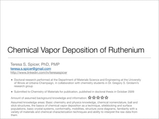
1. Chemical Vapor Deposition of Ruthenium
Teresa S. Spicer, PhD, PMP
teresa.s.spicer@gmail.com
http://www.linkedin.com/in/teresaspicer
• Doctoral research performed at the Department of Materials Science and Engineering at the University
of Illinois at Urbana-Champaign, in collaboration with chemistry students in Dr. Gregory S. Girolami’s
research group
• Submitted to Chemistry of Materials for publication, published in doctoral thesis in October 2009
Amount of assumed background knowledge and information:
Assumed knowledge areas: Basic chemistry and physics knowledge, chemical nomenclature, ball and
stick structures, the basics of chemical vapor deposition as a technique, siteblocking and surface
populations, basic crystal systems, conformality, mobilities, structure zone diagrams, familiarity with a
variety of materials and chemical characterization techniques and ability to interpret the raw data from
them
2. Outline
Introduction
Problem Statement
Experiments
Results
Key Findings
4. Integrated circuits have created a vital industry and
enabled the telecommunications revolution
Global Semiconductors Market Value, $ billion, 2004-2013(e)
350 9
J 8
Market value (USD billions)
300
7
250 J
J J 6
J
% Growth
200 5
J
150 4
J
3
100 J
J 2
50
1
0 0
2004 2005 2006 2007 2008 2009 2010 2011 2012 2013
Source: Datamonitor
Image from http://www.textually.org/
Semiconductor industry plays an important role in globalization,
and therefore also in shaping our collective future.
5. Miniaturization drives integrated circuit development
and applications
Image from http://tunicca.wordpress.com/2009/07/21/moores-law-the-effect-on-productivity/
6. Materials and thin film processing are key to
miniaturization
2007: 30 new materials introduced into 45-nm node1
1 A Thorough Examination of the Electronic Chemicals and Materials Markets, Businesswire, August 15, 2007
Image from http://www.intel.com/pressroom/kits/45nm/photos.htm
❝The implementation of high-k and
metal materials marks the biggest
change in transistor technology
since the introduction of polysilicon
gate MOS transistors in the late
1960s.❞
Gordon Moore, Intel Co-Founder, regarding two of the 30
new materials introduced in 2007
In order to continue miniaturization,
thin films of new materials are required.
7. As devices shrink in area, conformal deposition
becomes a new challenge
} ttop
The ideal: completely conformal (uniform), fast coating.
Conformality = (ttop/tbottom)·100%
} tbottom
Conformal coating.
The problem: the hole ‘clogs’ at the top - pinch-off.
Pinch-off.
The impractical compromise: grow slowly so that the
hole doesn’t have time to pinch off.
Conformal coating, but slow growth.
An opportunity exists to find a process that is fast
but retains the uniformity of the coating.
8. DRAMs and interconnects need conformal Ru
deposition
Future dynamic random access memories
• Ru is electronically like Pt, which was used in initial
research
• Unlike Pt, Ru etches easily in mass production
Kim, K., and Lee, S. Y., Microelectronic Engineering, 2007. 84: p. 1976-1981.
Seed layer for electrodeposition filling of copper
• Cu electroplates onto Ru
• Ru adheres better to the TaN underneath than Cu ECD Ru seed
layer
Cu
Moffat, T.P., et al., J. Electrochem.Soc., 2006. 153(1): p. C37-C50.
9. Synthetic inorganic chemistry and materials
engineering are required for new CVD processes
Synthetic inorganic
Materials engineering
chemistry
Conception and synthesis of new
CVD of films from precursor
CVD precursor candidates
Process hypothesis
development
Synthesis of modified precursor Measurement of film properties
Development of novel growth processes and chemistry
are needed to develop good CVD processes.
11. Ruthenium catalyzes decomposition of organic
ligands even at low temperatures
Common case Desired case
H H
H H
H H
C C C
Ru Ru
Example:
1. Cyclohexadiene → benzene + H2
2. Benzene → surface hydrocarbons
All MOCVD Ru precursors are susceptible
to severe carbon incorporation.
12. Due to this difficulty, Ru MOCVD growth rates are
generally low
Resistivity Growth Rate Conformality Grows on
Molecule C%
(μΩ·cm) (nm/min) previous layer?
(C6H6)Ru(C6H8)1 <1% - 2% 12-24 ? ? ✓
(1,5-COD)Ru(C7H9)2 1% - 3% ? 0.28 ? ✓
Ru(EtCp)2 3,4 ? ~7-150 ? ? ✓
RuCp(i-PrCp)5 ? 12-13 7.5-20 ? ✕
1 Choi, J., et al. Japanese Journal of Applied Physics, 2002. 41(11B): p. 6852-6856; Schneider, A., et al., Chemical Vapor Deposition, 2007. 13(8): p. 389-395.
2 Schneider, A., et al. Chemical Vapor Deposition, 2005. 11(2): p. 99-105.
3 Aoyama, T. and K. Eguchi. Japanese Journal of Applied Physics, Part 2 (Letters), 1999. 38(10A): p. 1134-6.
4 Matsui, Y., et al. Electrochemical and Solid-State Letters, 2002. 5(1): p. C18-C21.
5 Kang, S.Y., et al. J. Electrochem. Soc., 2002. 149(6): p. C317-C323.
Advances in Ru MOCVD need to be precursor chemistry-driven.
13. Surface science suggests choosing an appropriate
ligand set can minimize ligand decomposition
• Low benzene coverages inhibit benzene
Desired case decomposition on Ru1
• CO does not dissociate readily on Ru2
• When CO and benzene are co-adsorbed:
O O O
‣ CO acts as a spacer between the
C C C benzene molecules3
‣ CO halves the saturation benzene
Ru coverage3
1 Jakob, P. Doctoral Dissertation, Teknische Universität München, 1989.
2 Jakob, P. nd Menzel, D. Surf. Sci. 210, 1988, 503-530.
3 Heimann, P. A. et al, Surf. Sci. 210, 1989, 282-300
Ligands that result in CO and benzene co-adsorbed on Ru may
circumvent the catalytic decomposition.
14. Tricarbonyl(1,3-cyclohexadiene)Ru(0) is expected to
give benzene and CO co-adsorbed on the surface
Expected Consequences:
• Very low carbon incorporation
• Conformal growth due to siteblocking
H
H
O O O O
C C C C
Ru
Ru
1,3-cyclohexadiene and CO as Ru ligands could naturally give
clean and conformal deposition.
18. Reaction products were analyzed with NMR
Condensation of reaction
products
• Film deposition run in specialty glassware
• Products captured in chilled NMR tube
19. The likely decomposition reaction is
(C6H8)Ru(CO)3 → H2 + C6H6 + 3CO
1H NMR Spectrum of Reaction Products
CHCl3 (solvent)
H2O (present initially)
Benzene
Missing 1,3-cyclohexadiene peaks
7 6 5 4 3 2 1 PPM
Toluene multiplets
(synthesis solvent) Toluene methyl group
(synthesis solvent)
20. The activation energy is 17 ± 7 kJ/mol
500°C 400°C
Growth rate: 2 - 24 nm/min
Decomposition temperature: 80°C
300°C
Precursor pressure: 0.030 mTorr
200°C
The low activation energy of the decomposition
reaction makes low-temperature deposition possible.
21. The Ru films are crystalline at all temperatures
200°C
500°C
Typical amorphous material
At both high and low growth temperatures,
the films show clear crystallinity.
22. The microstructures are compact
Ru film
Ru film
SiO2
Si substrate
Si substrate
206 nm Ru on SiO2, 350°C 216 nm Ru on Si, 460°C
The lack of the usual visible gaps or
holes in the films helps improve resistivity.
23. At low temperatures, kinetics rather than driving
forces determine both microstructure and texture
For Ru
Zone I: RT - 500 ºC
Zone II: 500 ºC - 1030 ºC
Zone III: 1030 ºC - 2334ºC
H
H
O O O O
C C C C
Ru
Ru
Energy minimization does not play a large role in low-
temperature ( > 500 ºC for Ru) texture.
24. ation of any in-plane textureintensity of reection i a reasonable oriented sample. In most case
was not possible in in a randomly
The films exhibit c-plane fiber texture at low
me for any of the films tried.more than one preferred orientation. (0 0 0 1) was the most preferr
Pole figure intensities were too low
information. However, the out-of-planein almostwasfilms grown at temperatures below 350 C
orientation texture all quantified ◦
temperatures
g texture coefficients for each resolved reflection. Texture 350 C. The overall degree of textu
prominence diminished above ◦
re defined as[123, 124] films, σ, was computed from a close analogue to the standard dev
Texture coefficients: Overall degree of texture:
Ii N
N I0 (Ci − Ci0 )2
Ci = N I , σ = (3.1) ,
i=1
i
i=1
N
I0
is the texture coefficient for reflection CiN is theare defined as in equation 3.1 and Ci0 is the te
where i, and N number of
}
• Increasing texture in thicker compared toi, and i0 is the
sidered, Ii is the intensity incoeffcient of a peak in aIrandomly oriented film. As can quickly be
film of reection
thinner films
eection i in a randomly orienteddenition, σ is zero cases,randomly texture forms during of 1 o
The
the sample. In most for a lms had oriented film. σ values
• Texture of T modulated films determined by
ne preferred orientation. (0 0 0 1) was the most preferred thickening
final growth temperature
n almost all films grown at temperatures below 350 ◦ C, while its 39
diminished above 350 ◦ C. The overall degree of texture in the
computed from trends on all substrates standard deviation Role of substrate minimal
• Same σ a close analogue to the as
N
below T*=0.24
• (0001) fiber texture(Ci − Ci0 )
2
σ= , (3.2)
N Two different formation
• (1122), (0001), and (1011) preferred
i=1
mechanisms
orientations above
and N are defined as in equation 3.1 and Ci0 is the texture
25. The films can grow on many materials types
The films grow readily on several oxides and silicon.
26. The films grow very well on oxides
2 µm
32s Growth at 300°C
on thermally grown SiO2
1 µm
Root-mean-square roughness:
1.3 nm
~2300 nuclei/µm2
0 µm
0 µm 1 µm 2 µm
The films start growing very quickly and evenly on oxides.
27. Contrary to expectation, the 1,3-CHD ligands
decompose to carbon fragments
TOF - ERDA Elemental Composition Catalytic activation of C-C bonds likely occurs
H
H
H H
C C C
Ru
The adsorption behavior seen in surface science studies does
not prevent ligand decomposition in a CVD process.
28. Traditional CVD has a high reaction probability
Traditional CVD O
(at high temperatures) C
O
Ru C C
C C O
O O
C
C O
C
C
O
Ru
O
Ru
O
Traditional CVD often leads to pinch-off.
29. If the incoming molecules do not stick or react
where they first land, conformality is possible
High sticking probability Low sticking probability
Precursor Nearly conformal
Precursor The deposited
atoms quickly molecules bounce coverage.
molecules react
cause pinch-off. off the walls into
or stick nearly
the trench.
instantly
If the incoming molecules don’t stick immediately, coatings are
more likely to be uniform.
30. Conformality was measured using a macrotrench
experiment
Conformality and sticking
coefficient determination
Silicon
• Film grown in macrotrench at 0.50 mTorr
Ta foil
• Conformality directly calculated from Silicon
thickness profile
• Sticking coefficient and growth rate
dependence on pressure calculated
Cross-section → thickness profile
31. The process is very conformal due to siteblocking
Temperature: 300°C
~90% Pressure: 0.5 mTorr
~75% GR on flat surface: 10 nm/min
Simulations1:
75% conformality in a macrotrench
90% conformality in a closed hole
1 Yang, Y.; Jayaraman, S.; Kim, D.Y.; Girolami, G. S.;
Abelson, J. R., Chem. Mat. 2006, 18, 21, 5088-5096.
As predicted, the conformality of the process is good
and the sticking coefficient is low.
33. Chemical Vapor Deposition of Ruthenium
• Facile reaction
• CO does not stop catalytic dehydrogenation of 1,3-CHD
• The ligands on the surface cause siteblocking, which makes the
process very conformal
34. Acknowledgements
Dr. Charles Spicer, UNCC
Dr. Bong-Sub Lee, UIUC
Kristof Darmawikarta, UIUC
Dr. Angel Yanguas-Gil, UIUC
Dr. Mauro Sardela, UIUC
Nancy Finnegan, UIUC (Ret.)
Dr. Tim Spila, UIUC
Dr. Richard Haasch, UIUC
Subhash Gujrathi, Université de Montreal
Research supported by NSF grant DMR-0420768
Film characterization was carried out in the Center for Microanalysis of Materials,
University of Illinois, which is partially supported by the U.S. Department of
Energy under grant DEFG02-91-ER45439